background image

81

PDR-W839

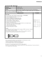
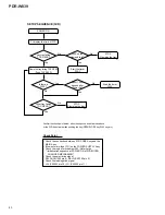
POWER ON

Each mechanism SW is checked.

MECHA SW

• SELINIT SW

(pin 4)

• SEL SW

(pin 5)

• OPEN SW

(pin 90)

• CLOSE SW

(pin 91)

• CLAMP SW

(pin 6)

• HOME SW

(pin 7)

Mechanism SW logic

at HOME position

at CLAMP position

• SELINIT SW

"L"

"L"(clamp tray1) /"H"(clamp tray2,3)

• SEL SW

"L"

"L"

• OPEN SW

"H"

"H"

• CLOSE SW

"L"

"L"

• CLAMP SW

"H"

"L"

• HOME SW

"L"

"L"

Initialization Sequence at POWER ON of 3CD MICRO CHANGER MECHANISM

Setting the initial condition for shipping

Setting the initial operating condition

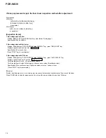
The factory default settings shall be as below. 
For reason that this product memorizes the condition of below items by back-up battery.

Note) All items are reset to the factory default setting when pushing the MENU key about 10 sec.

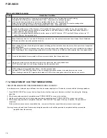
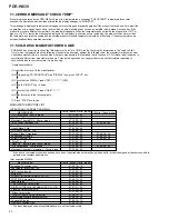
Adjusting the shipping position of  mechanism. 
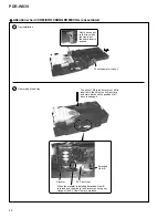
Before shipping, it is necessary to adjust the shipping position of the mechanism. See following. 
 
< CD-R tray mechanism > 
1.  Open CD-R tray and remove a disc.
2.  Push OPEN/CLOSE button and wait until  the FL display "NO DISC".
 
< 3CD changer mechanism > 
1.  Open the tray; CD1–CD3, and remove all discs . And close the tray.
2.  Wait until DISC1 to 3 indicators on the FL display, see right, are put out all
     and the mechanism is stopped.
3.  ON pushing "STOP(CD-R side)" key, and push "PLAY MODE" key . 
     

=

  "OK!" is displayed on the FL display, then the mechanism is set to the shipping position.

4.  Turn off the power.

Item Initial 

condition

REC volume(Analog)

0dB

REC volume(Optical)

0dB

REC volume(Coaxial)

0dB

REC volume FIX(Analog)

ON

REC volume FIX(Optical)

ON

REC volume FIX(Coaxial)

ON

INPUT SELECTOR

ANALOG

MENU
H.P. LEVEL

L

A.TRACK

ON

A.LVL(Analog)

-54dB

A.LVL(Optical)

-54dB

A.LVL(Coaxial)

-54dB

FADER(Analog)

5sec

FADER(Optical)

5sec

FADER(Coaxial)

5sec

T.INC

OFF

BALANCE(Analog)

center

BALANCE(Optical)

center

BALANCE(Coaxial)

center

DISC

DISC

DISC

1

2

3

Summary of Contents for PDR-W839

Page 1: ...IS OF CD R CORE ASSY 87 7 2 PARTS 88 7 2 1 IC 88 7 2 2 DISPLAY 102 8 PANEL FACILITIES AND SPECIFICATIONS 104 Type Model Power Requirement Remarks PDR W839 KUXJ CA AC120V WYXJ AC220 240V WVXJ AC220 240V THIS MANUAL IS APPLICABLE TO THE FOLLOWING MODEL S AND TYPE S FOR U S MODELS NECESSARY INFORMATION FOR DHHS RULES MARKED ON THE REAR BASEAND ON THE TOP OF CD MECHANISM AS BELOW DANGER LASER RADIATIO...

Page 2: ... evident from visual inspection nor the protection afforded by them necessarily can be obtained by using replacement components rated for voltage wattage etc Replacement parts which have these special safety characteristics are identified in this Service Manual Electrical components having such features are identified by marking with a on the schematics and on the parts list in this Service Manual...

Page 3: ... A SPECIALLY INSTRUCTED PERSON LASER DIODE CHARACTERISTICS MAXIMUM OUTPUT POWER 5 mW WAVELENGTH 760 800 nm 1 Laser Interlock Mechanism The position of the switch S101 on the SELECT UNIT for detecting clamping state is detected by the system microprocessor and the design prevents laser diode oscillation when the switch S101 is not on CLMP terminal side CLMP signal is OFF or high level Thus the inte...

Page 4: ...1 PACKING PARTS LIST Mark No Description Part No 2 EXPLODED VIEWS AND PARTS LIST NOTES Parts marked by NSP are generally unavailable because they are not in our Master Spare Parts List The mark found on some component parts indicates the importance of the safety factor of the part Therefore when replacing be sure to use parts of identical designation Screws adjacent to mark on the product are used...

Page 5: ... 3 FRONT PANEL SECTION 5 4 39 39 39 39 32 25 17 39 KUXJ CA Type Only 35 18 44 44 39 38 38 39 39 39 30 24 23 10 12 2 8 14 43 9 KUXJ CA Type Only KUXJ CA Type Only WYXJ and WVXJ Types Only 39 39 39 38 17 31 33 34 39 20 29 29 15 16 7 39 39 19 39 39 39 39 39 42 15 1 28 28 3 13 11 27 27 39 41 WYXJ Type Only 36 or 37 38 40 38 6 26 21 22 H D M A 2 2 EXTERIOR SECTION ...

Page 6: ...245 NSP 28 PCB Holder PNW2029 29 Insulator PNW2766 30 Tray Panel C PNW2936 31 Tray Panel B R PNW2981 NSP 32 Laser Caution Label See Contrast table 2 33 Getter W739 KU PRW1542 34 CDR Getter AAX7837 35 Disc Caution Label See Contrast table 2 36 Caution Label See Contrast table 2 37 Caution Label HE See Contrast table 2 38 Screw ABA1207 39 Screw BBZ30P080FCC 40 Screw PPZ30P080FMC 41 Caution Label See...

Page 7: ...able 2 12 Mode Button B PAC2011 13 Self Lighted Button PAC2023 14 Pioneer Badge PAM1776 15 Display Panel See Contrast table 2 16 LED Lens PNW2745 17 REC Ring PNW2795 18 Screw PPZ30P080FZK 19 Screw ABA7009 2 CONTRAST TABLE PDR W839 KUXJ CA WYXJ and WVXJ Types are constructed the same except for the following Mark No Symbol and Description Part No Remarks KUXJ CA Type WYXJ Type WVXJ Type 1 2 3 4 11 ...

Page 8: ...sm ASSY 1 2 NSP 1 LOAB Assy VWG2171 2 32P Flexible Cable 30V PDD1222 3 Connector Assy PG03KK E07 4 DC Motor LOADING PXM1027 5 Connector Assy 2P VKP2253 6 Motor Pulley PNW1634 7 Loading Motor Assy VXX2505 8 Clamper Plate VNE2162 9 Rubber Belt VEB1315 10 Loading Base S PNW2968 11 Tray VNL1858 12 Gear Pulley VNL1866 13 Loading Gear VNL1860 14 Drive Gear VNL1861 15 Drive Cam VNL1862 16 Lock Plate VNL1...

Page 9: ... View B Mark No Description Part No CD R CORE Mechanism ASSY 2 2 PARTS LIST 2 5 CD R CORE Mechanism ASSY 2 2 NSP 1 MECHA PCB Assy PWX1625 2 DC Motor SPINDLE PXM1044 NSP 3 DC Motor CARRIAGE PXM1045 4 Float Rubber PEB1308 5 Carriage Motor Assy PEA1353 NSP 6 Rack Spring DBH1285 NSP 7 Reflection Sheet PNM1325 8 Float Base PNW2964 9 Pinion Gear PNW2994 10 Gear A PNW2855 11 Gear B PNW2856 12 Gear C PNW2...

Page 10: ...ue Black 28 44 43 43 22 21 23 24 14 18 15 2 3 5 5 1 7 7 10 46 9 8 6 No 36 Sub Tray Part Column 2 2 2 2 Gutter 1 1 Gutter Shaft 1 Gutter 1 Boss 1 Gutter 1 1 Gutter Inside Rail 1 Inside Rail 2 Inside Gutter 1 1 Rail 2 Gutter 2 Bottom Gutter 2 Bottom Gutter Whole Left Front Under Gutter 37 45 E F G 2 6 3CD MICROCHANGER MECHANISM ...

Page 11: ...lt AEB7159 19 Elevator Base ANW7132 20 Tray Guide ANW7150 21 TG Stopper ANW7151 22 TG Spring ABH7175 23 Cam Plate ANW7147 24 Lock Lever ANW7148 25 Float Rubber A Blue AEB7063 26 Float Rubber B Black AEB7066 27 Float Base ANW7130 28 Clamper Holder ANW7152 29 Yoke ANG7257 30 Clamper Magnet AMF7001 31 Clamper SO XNW3007 32 Swing Base ANW7131 33 Main Tray ANW7133 34 Lock Plate ANW7144 35 Lock Plate Sp...

Page 12: ... LD A F M F T INSIDE SW LOADING MOTOR SELECT MOTOR SP SL LO 1 7 RFGO 25 14 16 TEO FEO FOO TRO FMO 10 3 8 15 14 13 16 A H 91 98 WR RFDC F FE TE RFAC RFWBL IC101 AK8567 RFPROCESSOR LD CONTROL CIRCUIT 89 88 10 9 80 39 43 39 41 50 52 19 FG 31 15 16 17 18 FCS TRK CN1 17 20 23 26 32 29 31 30 11 12 13 14 CN101 CN452 CN601 PC651 N PXM1044 PEA1353 VXX2505 JL5809K F1 FG Generator 48 17 2872MHz RFDC FG TE 65...

Page 13: ...TA 16 13 L R XT DACMCK XTI AOUTL AOUTR I IC701 LC75710NE FL DRIVER 64 63 62 FLD FLCL FLCE V701 FL DISPLAY Key Input REC VOL JOG with Push Button 1 2 67 25 18 2 7 2 7 CN302 CN502 3CDPLAY 3CDPLAY CD RPLAY CN601 IC809 CN904 CN901 CN701 C CN1301 N801 5 13 Headphone Keyboard IN CN1101 CN201 CN202 V 5A V 5D V 6P 3CD PLAY CD R PLAY CDR CORE ASSY CN901 POWER SUPPLY UNIT SR IN HEADPHPONE ASSY OPERATIG 1 3 ...

Page 14: ...C B LOAB ASSY VWG2171 MECHA PCB ASSY PWX1625 PDD1222 PG06KK F20 PDD1218 PDD1217 CN601 CN101 CN101 CN452 CN451 F F GNDS GNDA F B A H VCC VC G D C E GNDA VC FPDO V 5A V 5A CFREQ CMOD PGND VRDC VWDC2 VWDC1 GNDD OSCEN ODON W XR LDON T T POWER SUPPLY UNIT PWR1029 M CDR CORE ASSY PYY1286 A ...

Page 15: ...WU7432 MOTOR UNIT AWU7431 F E CN101 CN1302 J102 J102 J101 J101 PICKUP UNIT KSM213CCM PDD1214 KEY BOARD JACK PDE1309 PDD1215 H 1 3 H 3 3 MAIN ASSY KUXJ CA PWM2325 WYXJ WVXJ PWM2326 H OPERATING 1 ASSY KUXJ CA PWZ4133 WYXJ WVXJ PWZ4134 I OPERATING 2 ASSY KUXJ CA PWZ4141 WYXJ WVXJ PWZ4142 J OPERATING 3 ASSY KUXJ CA PWZ4149 WYXJ WVXJ PWZ4150 K HEADPHONE ASSY KUXJ CA PWZ4157 WYXJ WVXJ PWZ4158 3CD CORE A...

Page 16: ...PDR W839 16 A B C D 1 2 3 4 1 2 3 4 3 3 CD R CORE ASSY 1 5 1 5 A A 4 5 A 3 5 CD R CORE ASSY PYY1286 A 1 5 Regulator ...

Page 17: ...PDR W839 17 A B C D 5 6 7 8 5 6 7 8 1 5 A A 5 5 A 3 5 A 2 5 The power supply is shown with the marked box H 3 3 CN904 CN302 Mecha Control U com 1 3 2 4 5 6 7 8 10 9 ...

Page 18: ...PDR W839 18 A B C D 1 2 3 4 1 2 3 4 2 5 A R R A 1 5 A 4 5 A 1 5 CD R CORE ASSY PYY1286 A 2 5 R R CN101 CN1 11 12 3 4 CD R CORE ASSY 2 5 ...

Page 19: ...6 7 8 5 6 7 8 2 5 A F Rank 1 F Rank 1 A 3 5 A 1 5 A 4 5 A 5 5 A 3 5 A 1 5 A 4 5 CN102 TP_POINT RF PROCESSOR SIGNAL ROUTE RF SIGNAL OPTICAL SIGNAL COAXI AL SIGNAL AUDIO SIGNAL DIGITAL AUDIO SIGNAL REC OP CO D R 15 13 14 16 17 ...

Page 20: ...PDR W839 20 A B C D 1 2 3 4 1 2 3 4 3 5 A A 2 5 A 5 5 A 2 5 CD R CORE ASSY PYY1286 A 3 5 18 3 5 CD R CORE ASSY 3 5 ...

Page 21: ...PDR W839 21 A B C D 5 6 7 8 5 6 7 8 3 5 A A 1 5 A 2 5 A 4 5 A 1 5 Servo Amp IC Multiplexer ...

Page 22: ...PDR W839 22 A B C D 1 2 3 4 1 2 3 4 4 5 A EFM ENCODER A 1 5 A 5 5 A 1 5 OP CO 23 24 3 6 CD R CORE ASSY 4 5 ...

Page 23: ...W839 23 A B C D 5 6 7 8 5 6 7 8 4 5 A CN502 A 3 5 A 5 5 A 5 5 A 2 5 H 2 3 A 2 5 CD R CORE ASSY PYY1286 A 4 5 CN601 SIGNAL ROUTE AUDIO SIGNAL REC AUDIO SIGNAL DIGITAL R D D OP CO D D R R R D D D 20 19 21 22 ...

Page 24: ...Y PWX1625 C LOAB ASSY VWG2171 B PC651 NJL5803K F1 CARRIAGE MOTOR ASSY SLIDER PEA1359 DC MOTOR ASSY SPINDLE PXM1044 J601 CN601 CN101 S601 S101 LOADING MOTOR PXM1017 VKP2253 08FM 1 0ST CN452 CN451 CN453 R602 R651 240 5CH BTL Driver 27 26 25 F Rank 1 3 7 CD R CORE ASSY 5 5 MECHA PCB ASSY and LOAB ASSY B C ...

Page 25: ... B C D 5 6 7 8 5 6 7 8 5 5 A F rank 1 A 1 5 A 2 5 A 1 5 A 4 5 The power supply is shown with the marked box CN901 CN202 M SIGNAL ROUTE RF SIGNAL AUDIO SIGNAL DIGITAL D D D 28 GND reinforcement for radiation measures ...

Page 26: ...han 23 minutes Outer Absolute time is more than 23 minutes W CLV WOBBLECLV E CLV EFMCLV at DIGITAL LOCK at DIGITAL UNLOCK DIRERR IC501 pin 142 0V 5V at MUTE ON Audio Signal Not Output at MUTE OFF Audio Signal Output AMUTE CN502 pin 9 5V 0V XPFAIL CN302 pin 9 5V Note The encircled numbers denote measuring point in the schematic diagram 1 CN302 pin 1 MSI V 200mV div H 5msec div 2 CN302 pin 2 MSO V 2...

Page 27: ...LAY 19 IC501 pin 37 REWLDON V 200mV div H 1msec div REC RW 20 IC501 pin 38 WLDON V 200mV div H 1msec div REC 21 IC501 pin 45 ODON V 200mV div H 200nsec div REC 22 IC501 pin 48 WDAT V 200mV div H 200nsec div REC 23 IC501 pin 126 SPDO V 200mV div H 100µsec div REC 24 Foot of R583 ATFG V 200mV div H 20µsec div REC 25 CN452 pin 4 SL V 200mV div H 5msec div PLAY 26 CN452 pin 7 SP V 200mV div H 5msec di...

Page 28: ...3 G MOTOR UNIT AWU7431 E LOADING UNIT AWU7432 PICKUP UNIT KSM213CCM F CN101 S11B PH K S J102 J102 J101 J101 FOCUS SERVO LOOP LINE F L S S C C F F F T F T T T C C S S L L L TRACKING SERVO LOOP LINE T SPINDLE SERVO LOOP LINE S CARRIAGE SERVO LOOP LINE C LOADING SERVO LOOP LINE L CN1302 CN1101 D CN1301 D D ...

Page 29: ...US0 V 200mV div H 1msec div PLAY 6 CN1201 pin 13 BUS1 V 200mV div H 1msec div PLAY 7 CN1201 pin 14 BUS2 V 200mV div H 5msec div PLAY 2 IC1201 pin 55 DMO V 200mV div H 5µsec div Hi COPY 3 CN1201 pin 10 XCCE V 200mV div H 1msec div PLAY 8 CN1201 pin 15 BUS3 V 200mV div H 1msec div PLAY 4 CN1201 pin 11 BUCK V 200mV div H 10msec div PLAY 3CD CORE ASSY 1 2 D ...

Page 30: ...PDR W839 30 A B C D 1 2 3 4 1 2 3 4 3 9 3CD CORE ASSY D H Normal Speed L Double Speed 3CD CORE ASSY PWM2334 D E CN101 To PICKUP UNIT CN1302 CN1301 CN1101 STBY 5CH BTL Driver 1 ...

Page 31: ...PDR W839 31 A B C D 5 6 7 8 5 6 7 8 D Details and substitution are done by the part list 9607S 33F CN902 H 3 3 CN1201 RF SIGNAL AUDIO SIGNAL DIGITAL SIGNAL ROUTE Digital Servo IC 3CD D 2 3 4 5 6 7 8 D D ...

Page 32: ...PDR W839 32 A B C D 1 2 3 4 1 2 3 4 1 3 H 3 10 MAIN ASSY 1 3 CH CH 100P VF C1128 EXCEPT KU YB YB 1 1 1 at L853 H 3 3 H 2 3 H 2 3 H 2 3 Codec IC COPY D A D A A D D A A A ...

Page 33: ... From IC803 MBA FILM CQMBA R473 CH CH 1 KU type C455 STBY 100P 470P CH 100P C456 C1127 EXCEPT KU type MAIN ASSY 1 3 KUXJ CA PWM2325 WYXJ WVXJ PWM2326 H 1 3 H 2 3 H 3 3 IC810 2 2 IC810 1 2 E CN1301 CN801 SIGNAL ROUTE AUDIO SIGNAL DIGITAL D A AUDIO SIGNAL ANALOG A A A A A A A ...

Page 34: ...2 3 4 1 2 3 4 2 3 H 3 11 MAIN ASSY 2 3 R9631 MAIN ASSY 2 3 KUXJ CA PWM2325 WYXJ WVXJ PWM2326 H 2 3 M CN201 CN1101 CN502 CN601 H 1 3 H 3 3 H 3 3 A 4 5 H 3 3 H 3 3 H 3 3 H 1 3 1 2 3 4 6 5 7 8 10 9 11 12 13 D D D SIZE 2125 only ...

Page 35: ...PDR W839 35 A B C D 5 6 7 8 5 6 7 8 2 3 H YF Ceramic CKSRYF at L612 at L608 at L605 H 3 3 The power supply is shown with the marked box AUDIO SIGNAL DIGITAL SIGNAL ROUTE D ...

Page 36: ...U type C903 STBY CH 22P C905 EXCEPT KU type PCB Binder VEF1040 16MHz 2 KU type L809 DTL1058 0 R9809 0 R9810 L810 EXCEPT KU type 3 KU type R965 100 100 0 0 220 R966 R967 R968 R969 R970 R971 EXCEPT KU type MAIN ASSY KUXJ CA PWM2325 WYXJ WVXJ PWM2326 H 3 3 H 2 3 System Control U com ...

Page 37: ...T at L903 FUNCTION TYPES TWO OPTICAL DIGITAL INPUTS HI BIT LEGATO LINK CONVERSION DEMO INDICATION AVAILABLE FOR JAPANESE KEYBOARD RENTAL COPY XOPT D CN1201 I CN701 CN901 CN902 H 2 3 H 2 3 H 1 3 H 1 3 H 2 3 A 1 5 CN302 AUDIO SIGNAL DIGITAL SIGNAL ROUTE 14 15 D D D ...

Page 38: ...mV div H 200nsec div REC 5 CN601 pin 8 DACMCK V 200mV div H 20nsec div 11 CN601 pin 15 DADI V 200mV div H 5msec div 12 CN601 pin 23 CODATA V 200mV div H 500nsec div 14 15 CN901 pin 22 FLDI V 200mV div H 10msec div CN901 pin 21 FLCL V 200mV div H 10msec div 13 CN601 pin 25 COLAT V 200mV div H 5msec div MAIN ASSY H1 3 MAIN ASSY H3 3 8 CN601 pin 12 DABCK V 200mV div H 200nsec div 9 CN601 pin 13 DACDA...

Page 39: ...PDR W839 39 ...

Page 40: ...EAD PHONE OPERATING1 OPERATING2 and OPERATING3 ASSYS 330Ω 330Ω OPERATING 1 ASSY I KUXJ CA PWZ4157 WYXJ WVXJ PWZ4158 HEADPHONE ASSY L 1 2 CN801 H 1 3 To A J1301 CN1301 JA1301 Display IC FL Indicator Tube KUXJ CA PWZ4133 WYXJ WVXJ PWZ4134 I 1 2 L ...

Page 41: ...G 3 ASSY S709 0 OPEN CLOSE 3 S710 0 OPEN CLOSE 2 S730 0 OPEN CLOSE 1 S717 COPY START CD CD R S718 CD SELECT 3 S719 CD SELECT 2 S720 CD SELECT 1 S721 7 STOP S722 DISP S723 FF S724 6 PLAY PAUSE S725 41 REV S726 MENU DELETE S727 OPEN CLOSE S728 REC REC MUTE OPERATING 1 ASSY S711 NAME S712 AUTO SPACE S713 SYNCHRO S714 FINALIZE S715 ERASE S716 REC MODE KUXJ CA PWZ4141 WYXJ WVXJ PWZ4142 KUXJ CA PWZ4149 ...

Page 42: ...CEMENT FOR CONTINUED PROTECTION AGAINST RISK OF FIRE REPLACE WITH SAME TYPE AND RATINGS ONLY CAUTION CAUTION FOR CONTINUED PROTECTION AGAINST RISK OF FIRE REPLACE WITH SAME TYPE NO 215002 MFD BY LITTELFUSE INC FOR FU1 215002 AC IN L N FU1 2A 250V 215002 POWER SUPPLY UNIT PWR1029 M ...

Page 43: ...TION FOR CONTINUED PROTECTION AGAINST RISK OF FIRE REPLACE WITH SAME TYPE NO 491 800 MFD BY LITTELFUSE INC FOR IC3 491 800 marked parts Only these parts are supplied as service parts No FU1 Service Parts IC01 IC03 IC02 IC04 Part No 215002 2A 49101 6 1 6A 49101 6 1 6A 491 800 0 8A 49101 6 1 6A GNDA1 V 8A V 16A GNDA2 V 16A V 5K GNDM V 6M GNDD V 5D GNDFL VF 24 FL AC A FL AC B V 5A GNDA V 5D GNDD V 6P...

Page 44: ... parts of PCB and schematic diagrams is shown below 3 The parts mounted on this PCB include all necessary parts for several destinations For further information for respective destinations be sure to check with the schematic diagram 4 View point of PCB diagrams Symbol In PCB Diagrams Symbol In Schematic Diagrams Part Name B C E D D G G S S B C E B C E D G S B C E B C E B C E Transistor Transistor ...

Page 45: ...839 45 A B C D 1 2 3 4 1 2 3 4 B C 4 2 MECHA PCB ASSY and LOAB ASSY M M CARRIAGE MOTOR SPINDLE MOTOR MECHA PCB ASSY C MECHA PCB ASSY C LOAB ASSY B A CN451 A CN452 PNP1476 A PNP1476 A VNP1762 A SIDE A SIDE B ...

Page 46: ... 3 4 1 2 3 4 4 3 CD R CORE ASSY A PNP1477 B CDR CORE ASSY A SIDE A IC307 IC306 IC305 IC201 IC506 IC303 IC931 IC502 IC505 IC504 IC309 IC255 IC302 IC107 IC304 IC421 IC422 IC401 Q101 Q104 IC102 IC103 Q103 IC1161 IC308 Q205 IC507 ...

Page 47: ... 1 2 3 4 1 2 3 4 A PNP1477 B CN904 H SIDE B To CDR PICKUP To POWER SUPPLY ASSY CN101 C CN601 B CN601 H CDR CORE ASSY A IC503 Q502 Q273 IC501 Q202 IC301 IC206 IC207 Q402 IC251 IC253 Q401 IC252 IC254 Q201 IC310 IC101 IC451 ...

Page 48: ...PDR W839 48 A B C D 1 2 3 4 1 2 3 4 4 4 3CD CORE ASSY D ANP7532 D 3CD CORE ASSY D CN902 H CN101 E SIDE A To PICKUP UNIT To PICKUP UNIT ...

Page 49: ...PDR W839 49 A B C D 1 2 3 4 1 2 3 4 D ANP7532 D 3CD CORE ASSY D SIDE B IC1201 IC1302 IC1301 Q1301 IC1102 IC1101 Q1101 Q1201 ...

Page 50: ...PDR W839 50 A B C D 1 2 3 4 1 2 3 4 4 5 MAIN ASSY H MAIN ASSY H CN1201 D CN701 I To POWER SUPPLY ASSY CN1301 L ...

Page 51: ...PDR W839 51 A B C D 5 6 7 8 5 6 7 8 H PNP1480 C SIDE A CN502 A 301 CN302 A ...

Page 52: ...PDR W839 52 A B C D 1 2 3 4 1 2 3 4 H PNP1480 C IC802 IC801 Q801 Q405 Q483 Q401 Q402 Q404 Q484 Q492 IC1811 IC803 Q403 IC402 IC903 IC904 IC90 IC401 Q490 Q480 Q481 Q601 IC810 MAIN ASSY H ...

Page 53: ...PDR W839 53 A B C D 5 6 7 8 5 6 7 8 H IC601 Q492 Q401 Q428 IC1811 IC901 Q490 Q481 1 SIDE B ...

Page 54: ...PDR W839 54 A B C D 1 2 3 4 1 2 3 4 4 6 HEAD PHONE OPERATING1 OPERATING2 and OPERATING3 ASSY I J K PNP1481 A OPERATING3 ASSY K OPERATING2 ASSY J SIDE A ...

Page 55: ...PDR W839 55 A B C D 5 6 7 8 5 6 7 8 I L HEAD PHONE ASSY L OPERATING1 ASSY I CN801 H CN901 H To Key Board ...

Page 56: ...PDR W839 56 A B C D 1 2 3 4 1 2 3 4 I L HEAD PHONE ASSY L OPERATING1 ASSY I IC701 Q708 ...

Page 57: ...PDR W839 57 A B C D 5 6 7 8 5 6 7 8 I J K PNP1481 A OPERATING3 ASSY K OPERATING2 ASSY J SIDE B IC701 Q701 Q704 Q707 Q706 Q705 ...

Page 58: ...J50 CKSRYB471K50 C402 C408 C409 C878 Not used CKSRYB104K25 C903 C905 CCSRCH220J50 Not used C451 C455 C456 Not used CCSRCH101J50 R433 R434 RN1 16SE1800D RN1 16SE1801D R429 R430 RN1 16SE1800D RN1 16SE1002D R437 R438 RN1 16SE5601D RS1 16S0R0J R431 R432 RN1 16SE5601D Not used R435 R436 Not used RN1 16SE1002D R405 Not used RS1 10S100J R423 R424 RS1 16S0R0J RS1 16S102J R9401 R9809 R9810 RS1 16S0R0J Not ...

Page 59: ...D303 D451 D452 1SS355 D105 D202 D251 DA204K D252 MA704 D161 D162 D501 D503 RB521S 30 COILS AND FILTERS X301 32MHz PSS1024 X501 33 8688MHz PSS1025 L101 L1579 L302 L304 QTL1013 L401 L402 L501 L503 QTL1013 L507 L508 L511 L513 L514 QTL1013 L517 L521 L522 QTL1013 L509 L510 L515 L516 VTL1077 L518 L520 VTL1077 CAPACITORS C901 56µF 10V ACH7109 C129 CCSRCH100D50 C139 C304 C307 C309 C320 CCSRCH101J50 C104 C...

Page 60: ...or PKN1024 CN453 PH Connector S2B PH SM3 CN451 PH Connector S3B PH SM3 CN901 PH Connector S6B PH SM3 CN102 PH Connector S8B PH SM3 CN452 8P FFC Connecor VKN1300 CN302 9P FFC Connecor VKN1301 CN502 25P FFC Connecor VKN1317 KN901 Earth Plate VNF1109 MECHA PCB ASSY SEMICONDUCTORS PC651 NJL5809K F1 SWITCHES AND RELAYS S601 PSG1014 RESISTORS Other Resistors RD1 4PU J OTHERS J601 3P Jumper Wire D20PWW03...

Page 61: ...40 L801 L850 L901 OTL1040 L611 PTL1003 CAPACITORS C1126 C1501 C437 C438 CCSRCH101J50 C452 C456 C629 C908 C914 CCSRCH101J50 C917 CCSRCH101J50 C805 C806 CCSRCH121J50 C615 CCSRCH470J50 C627 C922 C924 C927 CEAT101M10 C1101 C1105 C1109 CEAT101M25 C435 C436 C803 C804 CEAT220M50 C827 C828 CEAT220M50 C831 C834 C837 CEAT221M10 C809 C810 C817 C818 CEAT221M16 C896 C897 CEAT221M16 C611 C617 CEAT221M6R3 C621 C...

Page 62: ... 3P Jumper Connector 52151 0310 CN701 22P FFC Connector 9604S 22C Remote Receiver Unit GP1U27X V701 FL Indicator Tube PEL1102 OPERATING2 ASSY SWITCHES AND RELAYS S704 S708 VSG1009 RESISTORS Other Resistors RS1 16S J OTHERS 3P Cable Holder 51048 0300 J703 Jumper Wire D20PYY0305E OPERATING3 ASSY SWITCHES AND RELAYS S709 S710 S730 VSG1009 RESISTORS Other Resistors RS1 16S J OTHERS 3P Cable Holder 510...

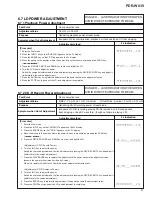
Page 63: ... do the LD ON and FOCUS ON movement 3 times 4 Redo the 3 movement once more 5 Confirm the FL display that the set detect NO DISC 1 Set the RW disc to the CD R side 2 Copy from 3CD side to CD R side at normal and double speed 3 Confirm the RF output and jitter level of 3CD side at normal and double speed 3CD CHECK NOTE There is no information to be shown in this 3CD adjustment Slider Gear 3CD Tray ...

Page 64: ... TQ82010 TQ82017 LE8010 by LEADER 2 Oscilloscope 3 CD Jitter Meter CD R ADJUSTMENT Mechanical point Electric point Mechanical point Electric point Mechanical point Electric point When EXCHANGE CD R CORE Mechanism Assy EXCHANGE CD R CORE PCB Assy Exchange Mechanism Assy CD R Pick up Exchange PCB CD R CORE PCB Assy Exchange Mechanism Assy Spindle Motor 6 7 LD Power Adjustment 6 8 Servo Adjustment Au...

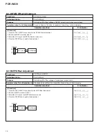
Page 65: ...de 6 6 2 Test Point NAME Pressing both the 3CD DISPLAY key and NAME key turn ON the POWER Continue pressing both the DISPLAY key and NAME key until the above DISPLAY appears Turn OFF the POWER and then turn ON the POWER again The state returnes to the Normal Mode CDR CORE ASSY A SIDE A 8 7 6 5 4 3 2 1 CN102 CN102 TP point 1 EQRF 2 RF 3 MPXO 4 MPP 5 TE 6 VC 7 ATFM 8 FE Front ...

Page 66: ... Adjustment data register 0 FINALIZE Focus servo ON ERASE Disc specification switch Continue pressing it more than three seconds and initialize the adjustment data SYNCHRO Execute the average adjustment AUTO SPACE Servo adjustment mode feed Key No Assignment Key Contents of Movement 1 0 OPEN CLOSE Tray Open Close 2 7 STOP LD power adjustment end Turn off the LD and disc selection set to CD 3 6 PLA...

Page 67: ...itial state is the coarse adjustment 7 Press the PLAY PAUSE key to register the adjustment if the power became the adjustment value assume the power when it was decided by A value When it is registered shift to the Overdrive power adjustment automatically Adjustment of CD R Overdrive Power 8 Turn the JOG key to adjust the power Switch the coarse adjustment and the fine adjustment by pressing the R...

Page 68: ... register the adjustment if the power became the adjustment value 12 Press the STOP key to goes out the LD and adjustment is completed 6 7 3 CD RW Record Power Adjustment RW Bias 2 3 mW 0 05 mW RW Rec 3 2 mW 0 05 mW RW Erase 5 2 mW 0 1 mW Pickup objective lens Optimizing CD RW recording power of laser diode Incapable of CD RW recording playing CD RWs recorded on it Sound pauses track skipping or b...

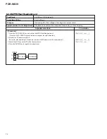
Page 69: ...oltage of focus error amplifier Focus in does not function or bad RF wave shape CN102 pin 8 Focus err Test Point Adjustment Value Purpose Symptom when Out of Adjustment Adjustment method FL Indication CN102 FE VC 8 6 10 1 prove Oscilloscope Procedure 1 Press the AUTO SPACE key and shift to the SRFO Offset Adjustment 2 Monitor the RFDC waveform with VC 2 Adjust the JOG key so that RFDC offset becom...

Page 70: ...ng Purpose Symptom when Out of Adjustment Adjustment method FL Indication CN102 RF VC 2 6 10 1 prove Oscilloscope Procedure 1 Press the AUTO SPACE key and shift to the MPP Offset Adjustment 2 Monitor the MPP waveform with VC 2 Adjust the JOG key so that MPP offset becomes zero 3 Press the ENTER key to register the adjustment 6 8 5 MPP Offset Adjustment 0 mV 50 mV CN102 pin 4 MPP Test Point Adjustm...

Page 71: ... the AUTO SPACE key and shift to the Tracking Gain MS MIX Adjustment 2 Move the Pickup to center of the disc by pressing the SCAN key 41 3 Monitor the MPX signal and set a CD disc 4 Press the FINALIZE key to FOCUS IN 5 Press the PLAY PAUSE key to turn the SPINDLE CAV 6 Adjust the JOG key so that MPX waveform MPP SPP becomes minimum 7 Press the ENTER key to register the adjustment 8 Press the STOP ...

Page 72: ...m in the readjustment 3 Adjust the JOG key so that TE offset becomes zero 4 Press the ENTER key to register the adjustment 6 8 8 MPP Offset Readjustment 0 mV 50 mV CN102 pin 5 Tracking err Test Point Adjustment Value Optimizing DC offset voltage of tracking error output circuit Playback does not function incapable of searching or track skipping Purpose Symptom when Out of Adjustment Adjustment met...

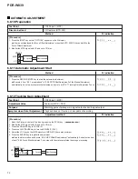
Page 73: ...EEPROM 11 Press the STOP key to stop the unit Caution In this adjustment shift to the RFDC Adjustment when pressing the ENTER key before step 9 and there is it when completed in normal on the indication However must not omit operation of steps 7 from 5 because RFDC is not adjusted to normal when pressing the ENTER key with the state that steps 7 from 5 are not executed The arbitrary value that mod...

Page 74: ...matic Adjustment Start Method FL Indication Procedure 1 Move the Pickup to center of the disc by pressing the SCAN key 41 2 Monitor the MPX signal with VC and set a CD disc 3 Press the FINALIZE key to FOCUS IN 4 Press the PLAY PAUSE key to turn the SPINDLE CAV 5 Adjust the JOG key so that MPX waveform MPP SPP becomes minimum 6 Press the ENTER key to register the adjustment Stop the disc rotation a...

Page 75: ...on the indication However must not omit operation of steps 5 from 3 because RFDC is not adjusted to normal when pressing the ENTER key with the state that steps 5 from 3 are not executed How to execute the automatic adjustment once again after the automatic adjustment is completed 1 Press the STOP key to stop the disc rotation servo OFF 2 Press the AUTO SPACE key and shift to the Focus Offset adju...

Page 76: ...pears in about 4 sec like C1 Specification 65 pieces or less Press STOP key to reset display 3 Recording playback ATIP error Method While pushing CD R CONTROL side DISPLAY key press AUTO SPACE key Display appears in about 10 sec like ATIP The three digits on the left Total number of errors The three digits on the right Maximum continuous error number Specification item Specification Max continuous...

Page 77: ...cked disc The optimum recording power cannot be obtained Trouble in RF detection Defective laser diode Trouble in RF detection Defective RFT RFB circuit Recording power is not sufficient Improper soldering pattern short Trouble with power supply Unable to read ATIP or subcode IC201 PA9007A IC101 AK8567 IC308 TC7S14F F The unit stops during playback or recording Defective pickup Unable to focus bec...

Page 78: ...t If searching for the writing starting position fails it is retried 19 times and if both are still incomplete then the operation halts F Once disk discrimination is completed and focus in action is failed then the operation halts A If the pick up jump occurs during recording and it is not recovered then the operation halts If ATIP data is not read for 4 sec during recording then the operation hal...

Page 79: ... on the CD R CORE Assy XPFAIL H normal Check the communication between the mechanism cont roller and each LSI MSI MSO MSCK EECS AD0 7 XRD XWR ASTB When FL does not turn on at all Check the connection between the MAIN Assy and OPERATING 1 Assy Check the communication lines FLDI FLCL FLCE and FLRST between the system controller IC901 and FL driver IC701 FL Driver IC701 on the OPERATING1 Assy breaks ...

Page 80: ...CN1302 pin 10 LO CN1302 pin 11 POWER ON FL display the time 0f 3CD Clamp the tray failing TOC READ Doing TOC READ Any tray failing TOC READ Other tray failing TOC READ Is there a DISC DISC on the clamped tary About 15sec passed after Power On Yes Yes Yes Yes Yes STOP Clamping the tray STOP Clamping the tray Start the timer PLAY Start the timer PLAY No No No No No SETUP SEQUENCE 3CD Check Point Con...

Page 81: ...to adjust the shipping position of the mechanism See following CD R tray mechanism 1 Open CD R tray and remove a disc 2 Push OPEN CLOSE button and wait until the FL display NO DISC 3CD changer mechanism 1 Open the tray CD1 CD3 and remove all discs And close the tray 2 Wait until DISC1 to 3 indicators on the FL display see right are put out all and the mechanism is stopped 3 ON pushing STOP CD R si...

Page 82: ... the manufacturer 2 While pushing CD R CONTROL side DISPLAY key press INPUT key 3 Check that the DISPLAY reads PEC RID 4 Press the INPUT key 14 times 5 Check that the DISPLAY reads LIA 97 6 Refer this value to the following table 7 Press STOP key to end MANUFACTURER CODE LIST OPERATION CONFIRMATION MEDIA MEDIA MAKER Ritek Co 80min group TDK Corporation 80min group Taiyo Yuden Company Ltd Mitsubish...

Page 83: ...5 7 5 CD R CORE Assy Bridge Tray 7 1 6 DISASSEMBLY Diagnosis of 3CD Microchanger Mechanism CN101 CN451 CN452 Remove four connectors CN453 POWER 1 1 Tray Open Tray Close 4 Changer section OPEN CLOSE Bonnet Tray Panel C Tray Panel R 6 5 6 3 2 5 3 5 2 3 4 4 1 4 5 2 Recorder section OPEN CLOSE Bonnet CD R CORE ASSY Servo Mechanism Assy Unhook 9 8 2 4Wick Cable 3Wick Cable ...

Page 84: ...e four connectors Bottom view Top view 3CD Microchanger Mechanism 2 3 3 1 2 1 2 4 9 4 2 3CD MICROCHANGER MECHANISM 3CD Microchanger Mechanism Power Button B 13 14 15 SUB Tray x 3 Hook x2 is removed and the elevator the elevator cover the gear shaft and the loading gear are removed A sub tray becomes free ...

Page 85: ...5 PDR W839 The Hook is removed The bottom of a main tray is lifted Hook take off Main Tray Hook Mecha Base Float Base Swing Base Clamper Holder PICKUP UNIT Blue Black 17 16 19 18 20 21 22 23 Bottom View ...

Page 86: ...the home lever is opened The stopper arm is shut The stick of Ø3 plus driver etc of 0 is inserted in the hole of sub three trays and main trays and the position of all trays is arranged Extended Gear B EV Cam Gear Elevator When the elevator is installed Extended Gear B is turned and the ditch in the Elevator and the gear flange of the EV Cam Gear are matched ...

Page 87: ...ECHA PCB Assy 8P FFC 30v PDD1225 1 2 CN502 CN601 MAIN Assy 25P FFC PDD1227 3 CN302 CN904 MAIN Assy 9P FFC PDD1226 4 CN101 CN1 CD R Pickup 32P FFC PDD1224 5 CN451 CN101 LOAB Assy Connector Assy 3P PG03KK E50 6 1 6 CD R CORE Assy Other Assys 1 2 3 4 5 6 7 1 8 DIAGNOSIS OF CD R CORE ASSY 7 1 7 DIAGNOSIS OF 3CD MICROCHANGER MECHANISM and MAINASSY When diagnosing the CD R CORE Assy use the following Fl...

Page 88: ... R X 7 6 P W R X O L W R D C H R D C D C t u p t u o g n i s r e v e r W R D C 1 2 Q R D L H T I A W X 6 6 P C E D K O L C O d n a m m o c Q 5 8 5 2 D X C r o f t u p t u o K C O L C 2 2 R W X 5 6 P R W X O y r o m e m l a n r e t x e e h t f o n o i t a r e p o d a e r r o f t u p t u o l a n g i s e b o r t S 3 2 D R X 4 6 P D R X O y r o m e m l a n r e t x e e h t f o n o i t a r e p o e t i r...

Page 89: ... e w o l F R Playback Playback 1 6 5 I N A 5 7 P T F R A I t u p n i e p o l e v n e t r a p r e p p u F R 2 6 6 I N A 6 7 P 1 1 M A I e e r g e d n o i t a l u d o m r o f t u p n i g n i l p u o c t u o h t i w e p o l e v n e t r a p r e p p u F R 1 R M R D C n o i t a l u c l a c 3 6 7 I N A 7 7 P Y A R T A I L N E P O t u p n i N O I T I S O P G N I D A O L 4 6 d d v A d d V A V 5 5 6 1 f e r...

Page 90: ... 2 C D R V O d a e R r o f t pin u p t u o l o r t n o c r e v i r d r e s a L 1 2 N C D R V I p pin for Read m a l o r t n o c r e v i r d r e s a L p pin for Write m a l o r t n o c r e v i r d r e s a L 2 2 2 N C D R V I Laser driver time constant setting pin for Read Laser driver time constant setting pin for Write 3 2 F E R W O I tting voltage input pin for write APC built in DAC seting volta...

Page 91: ... sample L hold 1 6 R T F R P S I 2 6 W S D W V I switch control signal input pin for Write H ON L OFF switch control signal input pin for Read H ON L OFF t n a t s n o c e m i t r e v i r d r e s a L 3 6 W S D R V I t n a t s n o c e m i t r e v i r d r e s a L 4 6 A T E B S R I circuit reset pin H PHBETA BHBETA output to Reset t n e m e r u s a e m ß 5 6 K L C S I pin for register setting pin for...

Page 92: ...in u p n i A l a n g i s m a e b n i a M 2 9 N I B I t pin u p n i B l a n g i s m a e b n i a M 3 9 N I C I t pin u p n i C l a n g i s m a e b n i a M 4 9 N I D I t pin u p n i D l a n g i s m a e b n i a M 5 9 N I E I t pin u p n i E l a n g i s m a e b n i a M 6 9 N I F I t pin u p n i F l a n g i s m a e b n i a M 7 9 N I G I t pin u p n i G l a n g i s m a e b n i a M 8 9 N I H I t pin u p n...

Page 93: ...I Input of CH1 Input of CH2 9 1 D N G Substrate ground 6 2 N I 0 2 4 3 C C V W O P Power unit power supply input terminal CH3 CH4 7 C C V E R P Pre and loading unit power supply input terminal Power unit power supply input terminal 1 2 E T U M Input for mute control Output of CH3 OP AMP Output of CH4 OP AMP Inverting iutput of CH3 OP AMP Inverting iutput of CH4 OP AMP Not inverting iutput of CH3 O...

Page 94: ...94 PDR W839 Pin Function 1 5 PDC069 CD R CORE ASSY IC501 Encoder IC ...

Page 95: ...95 PDR W839 Pin Function 2 5 ...

Page 96: ...96 PDR W839 Pin Function 3 5 ...

Page 97: ...97 PDR W839 Pin Function 4 5 ...

Page 98: ...98 PDR W839 Pin Function 5 5 ...

Page 99: ... FLASH D X T 1 D X T H S A L F I e t i r w h s a l F d e s u t o N 2 3 at FLASH D X R 1 D X R H S A L F I 3 3 at FLASH K L C 1 K L C H S A L F I 4 3 at FLASH S T R 1 S T R H S A L F O 5 3 0 D X T O r e l l o r t n o c MECHA MECHA MECHA e h t h t i w t u p t u o n o i t a c i n u m m o c l a i r e S 6 3 0 D X R I r e l l o r t n o c e h t h t i w t u p n i n o i t a c i n u m m o c l a i r e S 7 3 ...

Page 100: ...t High Bit existence H High Bit exist DEMO display select SW Key Board select SW Internal External input OP amp change SW CE at FLASH Clock output for EEPROM Data output for EEPROM D IN 2 select SW for ELITE model H 2 Rental copy existence select SW H rental copy exist Simultaneous recording ON OFF SW EEPCLK EEPDATA URAROKU O O O O O O O O O 3 4 3 5 P O 4 4 2 5 P O 5 4 1 5 P O 6 4 5 V DSM I e t i ...

Page 101: ...e 3CD mechanism loading drive control 3CD mechanism select drive control 3CD mechanism SW L CD tray open end 3CD mechanism SW L CD tray close end O 2 8 6 0 P O 3 8 5 0 P I O 4 8 4 0 P I O 5 8 3 0 P I O 6 8 2 0 P I O 7 8 1 0 P O 8 8 0 0 P I O 9 8 07 1 P 0 9 6 0 1 P I I 1 9 5 0 1 P 2 9 4 0 1 P O 3 9 3 N A 1 D A Y E K I t u p n i D A y e K 4 9 2 N A 3 D A Y E K I 5 9 1 N A 2 D A Y E K I 6 9 S S V A S...

Page 102: ...102 PDR W839 7 2 2 DISPLAY PEL1102 OPERATING 1 ASSY V701 FL Display Pin Assignment Anode and Grid Assignment External Dimensions ...

Page 103: ...103 PDR W839 ...

Page 104: ...8 REC REC MUTE Press to put the recorder into record pause mode ready for recording Once recording use to record blank sections onto a disc 9 POWER OFF ON Press to switch the unit on or off 10 3 CD Controls 41 Press for reverse track skip press and hold for fast reverse playback Press for forward track skip press and hold for fast forward playback DISPLAY Use to switch the CD display mode 6 Press ...

Page 105: ... to select and play disc 1 2 or 3 from the changer CD R Switch to the CD recorder and play the currently loaded CD CD R CD RW 10 Playback skip buttons PROGRAM Program the playback track order CHECK Check the tracks of a programmed play list and monitor the CD changer CLEAR Clear the last programmed track in program play mode RANDOM Start random track disc playback REPEAT Set the repeat mode SKIPPL...

Page 106: ...ogram play mode SKIP ON Lights to indicate that a track s skip ID is set SKIP blinks when clearing or setting a skip ID ON does not appear VOL Lights when the digital volume level is set to something other than 0dB FIX Lights when fixed recording level is on DIG ANA Indicates whether internal recording is via a digital or analog link 5 REC THIS Hi COPY Lights when during CD recording and indicates...

Page 107: ...m wavelength 660 nm Frequency deflection Level 2 standard mode Recording specification values are for the LINE input analog 3 Input jacks Optical digital input jack Coaxial digital input jack Audio LINE input jacks Control IN jack 4 Output jacks Optical digital output jack Coaxial digital output jack Audio LINE output jack 5 Accessories Remote control unit 1 Size AA R6P dry cell batteries 2 Stereo...

Reviews: