PDP-LX5080D
61
5
6
7
8
5
6
7
8
C
D
F
A
B
E
5.2.7 AUDIO SYSTEM
Yes
No
No
No
Yes
Yes
No
No
Has the sound been emitted from
the speakers?
Yes
Has the sound been emitted from
the Audio out terminal?
Sound of all functions does not
output?
Yes
Yes
Check the speakers and speaker
cables. Is it no problem?
=> AU1
Is sound muting set?
Is the volume set to 0?
Is not headphone inserted?
Go to .
No
No
Check the cables (CN8806) from the main power and peripheral circuit.
Repair the failure points.
Pull out headphone, then check
again.
Replace the speakers or speaker
cables.
Cancel muting, then check again.
Yes
Raise the volume, then check again.
Is a voltage (+16.5 V) supplied to
IC9201?
Yes
No
Check the CN9251 and peripheral circuit.
Repair the failure points.
Is not a signal output from
CN9251? (pins 2, 4, 5, 7)
Yes
Check the IC9181 and peripheral circuit.
Repair the failure points.
Is a 12 V output from +12V_Reg
output of IC9181 normal?
Yes
Check the peripheral circuits and the communication with the
microcomputer and clock output of X9101.
If there was no ploblem replace the MSP5651M.
Are signals input to IC9151 and
IC9152?
(pins 2, 3, 5, 6)
Yes
Check the IC9151, IC9152 and peripheral circuit.
Repair the failure points.
Are signals output from IC9151
and IC9152?
(pins 1, 7)
No
Check between the LPF (L9255, L9256) and CN9251.
Repair the failure points.
Is not a PWM signal output from
IC9201?
(pins 34, 38, 46, 50)
Yes
Yes
No
Check between the input terminals and IC9101.
Repair the failure points.
Check the peripheral circuits and the communication with the
microcomputer and clock output of X9101.
If there was no ploblem replace the MSP5651M.
Is a signal input to IC9101?
(pins 24, 25)
No
No
Has I2C communication signal
arrived at IC9101?
B
A
Flowchart of Failure Analysis for The Audio System
42 43
44 45
No
Check around the IC9101.
Repair the failure points.
Is not a PWM signal output from
IC9101?
(pins 52, 53, 54, 55)
Yes
46 47
49 50
48
51
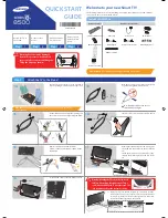
Summary of Contents for KURO PDP-LX508D
Page 19: ...PDP LX5080D 19 5 6 7 8 5 6 7 8 C D F A B E ...
Page 20: ...PDP LX5080D 20 1 2 3 4 1 2 3 4 C D F A B E 4 BLOCK DIAGRAM 4 1 OVERALL WIRING DIAGRAM 1 2 ...
Page 22: ...PDP LX5080D 22 1 2 3 4 1 2 3 4 C D F A B E 4 2 OVERALL WIRING DIAGRAM 2 2 ...
Page 23: ...PDP LX5080D 23 5 6 7 8 5 6 7 8 C D F A B E ...
Page 159: ...PDP LX5080D 159 5 6 7 8 5 6 7 8 C D F A B E ...
Page 170: ...PDP LX5080D 170 1 2 3 4 1 2 3 4 C D F A B E 10 6 PANEL CHASSIS SECTION ...