background image

CDJ-800

59

5

6

7

8

5

6

7

8

C

D

F

A

B

E

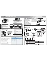
    Chart of a remote control unit function of CDJ-800

* Caution in the remote control unit use: Please connect to the DATA IN/OUT terminal before turning the power on.

Stop

Pause

Play

Invalidity

Invalidity

Invalidity

Invalidity

Invalidity

Invalidity

Invalidity

Invalidity

Invalidity

Invalidity

Invalidity

Invalidity

Search

Switch the Normal/Test mode

Invalidity

Eject

Audio playback 

REJECT

PAUSE

PLAY

STILL/STEP

– MULTI-SPEED +

SCAN

FUNC

CLEAR

AUDIO

SPEED

OPEN

7

8

9

4

5

6

VIDEO

STOP.M

START

1

2

3

DISPLAY

STILL

C-MODE

0

CR

SEARCH

FRAME

TIME

CHAPTER

A

B

C

Summary of Contents for CDJ-800

Page 1: ...elsele Belgium PIONEER ELECTRONICS ASIACENTRE PTE LTD 253 Alexandra Road 04 01 Singapore 159936 PIONEER CORPORATION 2002 CDJ 800 RRV2690 COMPACT DISC PLAYER CDJ 800 THIS MANUAL IS APPLICABLE TO THE FOLLOWING MODEL S AND TYPE S Model Type Power Requirement Remarks CDJ 800 KUCXJ AC120V CDJ 800 WYXJ AC220 240V For details refer to Important symbols for good services T ZZR OCT 2002 2002 printed in Jap...

Page 2: ...re often not evident from visual inspection nor the protection afforded by them necessarily can be obtained by using replacement components rated for voltage wattage etc Replacement parts which have these special safety characteristics are identified in this Service Manual Electrical components having such features are identified by marking with a on the schematics and on the parts list in this Se...

Page 3: ...is detected by the system microprocessor and the design prevents laser diode oscillation when the switch is not in LPS1 terminal side when the mechanism is not clamped and LPS1 signal is high level Thus the interlock will no longer function if the switch is deliberately set to LPS1 terminal side if LPS1 signal is low level In the test mode the interlock mechanism will not function Laser diode osci...

Page 4: ... improper lubrication or applying glue may lead to failures or troubles in the product By following the instructions in this manual be sure to apply the prescribed grease or glue to proper portions by the appropriate amount For replacement parts or tools the prescribed ones should be used 4 Shipping mode and shipping screws To protect the product from damages or failures that may be caused during ...

Page 5: ...3 MAIN ASSY 1 2 20 3 4 MAIN ASSY 2 2 22 3 5 AC IN TRNS SECB and REGB ASSYS 24 3 6 MFLB SLMB and KSWB ASSYS 26 3 7 JFLB SLDB and JOGB ASSYS 28 4 PCB CONNECTION DIAGRAM 35 4 1 MAIN ASSY 36 4 2 AC IN and TRNS ASSYS 38 4 3 SECB REGB and SLMB ASSYS 40 4 4 MFLB and KSWB ASSYS 42 4 5 SLDB JOGB and JFLB ASSYS 46 5 PCB PARTS LIST 50 6 ADJUSTMENT 54 7 GENERAL INFORMATION 55 7 1 DIAGNOSIS 55 7 1 1 SERVICE MO...

Page 6: ...305 W x 344 1 D x 108 5 H mm 12 5 8 W x 13 17 32 D x 4 1 4 H in 2 Audio section Frequency response 4 Hz to 20 kHz Signal to noise ratio 115 dB or more JEITA Distortion 0 006 JEITA 3 Accessories Operating instructions 1 Power cord 1 Audio cable 1 Control cord 1 Forced eject pin housed in a groove in the bottom panel 1 Warranty KUCXJ 1 NOTE Specifications and design are subject to possible modificat...

Page 7: ...CDJ 800 7 5 6 7 8 5 6 7 8 C D F A B E ...

Page 8: ...ent parts indicates the importance of the safety factor of the part Therefore when replacing be sure to use parts of identical designation Screws adjacent to mark on product are used for disassembly For the applying amount of lubricants or glue follow the instructions in this manual In the case of no amount instructions apply as you think it appropriate NOTES 5 8 7 6 9 11 12 KUCXJ type only 4 3 2 ...

Page 9: ...e 2 5 Polyethylene Bag Z21 038 6 Pad B DHA1556 7 Pad C DHA1557 8 Pad D DHA1558 9 Sheet RHX1006 10 Push Rod DEX1008 11 Pad A DHA1555 12 Packing Case See Contrast table 2 NSP 13 Warranty Card See Contrast table 2 NSP 14 Label VRW1629 Mark No Description Part No Mark No Symbol and Description Part No KUCXJ WYXJ 1 AC Power Cord ADG7021 ADG1154 4 Operating Instructions KUCXJ DRB1333 Not used 4 Operatin...

Page 10: ... I D C G E B A Refer to 2 3 CONTROL PANEL SECTION Refer to 2 4 SLOT IN MECHANISM SECTION 32 37 32 33 33 33 11 10 13 12 15 16 15 15 15 18 17 16 16 16 14 33 33 19 19 35 35 20 21 22 33 33 33 26 33 33 27 28 33 33 29 32 33 33 32 31 30 36 33 25 32 33 33 33 24 33 23 33 6 5 2 1 7 8 9 4 3 WYXJ type only ...

Page 11: ...6 18 Lead Card 16P DDD1221 19 Insulator Assy DXA1945 20 25P F F C 60V DDD1223 NSP 21 Silicon Rubber D5 L DEB1456 22 Bottom Cushion S4 DEC2506 23 Bottom Plate P DNH2531 24 Bottom Plate M DNH2546 25 Earth Plate DNH2532 NSP 26 Chassis See Contrast table 2 27 FU11 Fuse See Contrast table 2 28 Power Knob DAC2073 29 Heat Sink DNG1086 30 Trans Plate DNH2529 31 T21 Power Transformer See Contrast table 2 3...

Page 12: ... B F 1 H 2 J 4 K 5 I 3 45 46 46 46 46 46 46 46 46 40 49 41 42 48 43 39 44 47 46 46 46 46 46 49 49 31 30 29 28 27 26 49 46 36 34 32 35 35 35 37 38 46 31 23 46 25 46 1 1 1 1 1 1 1 1 1 Lubricaing oil ZLB PN397B 1 6 8 11 12 13 1 2 14 15 16 18 17 20 19 13 2 2 22 21 23 46 9 10 7 24 34 ...

Page 13: ...RELOOP Knob DAC2064 19 TEMPO Knob DAC2061 20 QUICK RETURN Knob DAC2070 21 CALL Knob DAC2062 22 VINYL Knob DAC2063 23 Earth Plate CU DBK1224 24 Slide Sheet 1C DAH1988 25 Vessel Sheet DEC2495 26 JOG B DNK4068 27 JOG Panel DAH2182 28 JOG Assy S DXX2521 29 JOG Plate DAH2052 30 JOG A DNK4067 31 Roller A Assy DXB1773 32 SW Ring DNK4070 33 34 SW Cushion HH48 DEC2523 35 SW Spring DBH1514 36 Sheet SW DSX10...

Page 14: ...7 15 16 27 3 26 30 26 30 29 12 9 22 13 33 21 To MAIN Assy Paint on side of axle Paint grease the inner surface of the wall Grease ZLB PN397B Grease ZLB PN397B Grease ZLB PN397B Grease ZLB PN397B Dyefree ZLX ME413A Dyefree ZLX ME413A Paint grease the inner surface of the wall Paint grease the inner surface of the wall 31 ...

Page 15: ...09 11 Yoke S4 DNH2528 12 Loading Lever DNK3406 13 Main Cam DNK3407 14 Disc Guide DNK3478 15 Clamp Arm DNK3576 16 Loading Base Assy S DEA1022 17 Eject Lever DNK3684 18 Lever AP DNK3835 19 Lever BP DNK3836 NSP 20 Worm Gear DNK3410 21 Loading Gear DNK3409 22 Drive Gear DNK3565 23 Clamper S4 DNK4072 NSP 24 DC Motor DXM1173 25 Vessel Cushion C DEC2457 26 Float Rubber S4 DEB1568 27 CD Mechanism DXA DA11...

Page 16: ...OO ADO TEI FEI A MAIN ASSY CD MECHANISM CN113 16P CN111 6P PICKUP ASSY SPINDLE MOTOR SLED MOTOR M LO LO V 7B LOADING MOTOR M M 4 7 9 14 1 4 11 14 3 CN122 25P CN56 19P CN53 25P CN51 11P CN22 11P CN11 T21 PT CN52 6P LOADING PHASE SW J91 6P CN54 2 1 24 1 1 2 1 2 3 1 3 25 6 4 2 1 11 9 11 9 7 2 8 V 11B 1 9 4 78 16MHz 28 61 5 IC113 BR24C64F EEPROM IC122 M51957BFP RESET IC G SLMB ASSY E REGB ASSY D SECB ...

Page 17: ...SSY H KSWB ASSY I JFLB ASSY K JOGB ASSY IC601 UPD16306B FL DRIVER V601 JOG FL SHEET SW CN501 19P CN110 ONLY DESIGNER USER CN502 6P CN1502 6P CN500 13P CN600 13P CN601 4P Slider VR CN1601 4P PANEL KEY PANEL KEY JOG ENCODER PANEL KEY CN503 11P CN602 3P CN1503 11P 16MHz 4MHz IC103 1 2 NJM4558MD 2 3 1 L DIGITAL OUT AUDIO OUT Serial data Serial data Latch clock ...

Page 18: ...DIAGRAM SLMB ASSY DWS1322 G TRNS ASSY DWR1364 C AC IN ASSY KUCXJ DWR1366 WYXJ DWR1363 B REGB ASSY DWR1362 CD MECHANISM DXA DA114 E MAIN ASSY DWG1563 A 1 2 A 2 2 A LOADING MOTOR ASSY S DXX2510 AKP7032 KUCXJ BKP1046 WYXJ AC POWER CORD KUCXJ ADG7021 WYXJ ADG1154 ...

Page 19: ...D F A B E SECB ASSY DWR1361 D KSWB ASSY DWS1321 H MFLB ASSY DWG1564 F SLDB ASSY DWS1323 J JOGB ASSY DWG1566 K JFLB ASSY DWG1565 I Note When ordering service parts be sure to refer to EXPLODED VIEWS and PARTS LIST or PCB PARTS LIST ...

Page 20: ...CDJ 800 20 1 2 3 4 1 2 3 4 C D F A B E 3 3 MAIN ASSY 1 2 A 1 2 A 2 2 A 2 2 A 2 2 A 2 2 A 2 2 A 2 2 A 2 2 A 2 2 A 2 2 ONLY DESIGNER USER ONLY DESIGNER USER DSS1139 AD D AD AD AD AD AD D ...

Page 21: ...A 2 2 A 2 2 A 2 2 MAIN ASSY DWG1563 TO CD MECHANISM TO CD MECHANISM FOCUS SERVO SIGNAL ROUTE RF SIGNAL ROUTE F F T T T T F TRACKING SERVO SIGNAL ROUTE T F F T T T F F T T RF RF RF AD DIGITAL OUT SIGNAL ROUTE D AUDIO DATA SIGNAL ROUTE 6 8 2 7 4 5 1 3 AD ...

Page 22: ...CDJ 800 22 1 2 3 4 1 2 3 4 C D F A B E 3 4 MAIN ASSY 2 2 A 2 2 A 2 2 A 1 2 A 1 2 A 1 2 A 1 2 MAIN ASSY DWG1563 GND GND GND GND GND GND GND GND GND GND GND GND GND GND GND GND GND GND AD AD AD ...

Page 23: ... 5 6 7 8 5 6 7 8 C D F A B E A 2 2 CN53 A 1 2 A 1 2 A 1 2 A 1 2 A 1 2 A 1 2 A 1 2 D The power supply is shown with the marked box AD DIGITAL OUT SIGNAL ROUTE D AUDIO DATA SIGNAL ROUTE AUDIO SIGNAL ROUTE AD D D D ...

Page 24: ...C AC IN ASSY KUCXJ DWR1366 WYXJ DWR1363 B FU11 KUCXJ 1 6A 125V REK1077 WYXJ T800mA L250V REK1021 LIVE NEUTRAL AC POWER CORD KUCXJ ADG7021 WYXJ ADG1154 KUCXJ DTT1169 WYXJ DTT1168 NOTE FOR FUSE REPLACEMENT FOR CONTINUED PROTECTION AGAINST RISK OF FIRE REPLACE WITH SAME TYPE AND RATINGS ONLY CAUTION ...

Page 25: ...CDJ 800 25 5 6 7 8 5 6 7 8 C D F A B E D E CN122 CN501 A 2 2 SECB ASSY DWR1361 D REGB ASSY DWR1362 E F CN1901 G The power supply is shown with the marked box ...

Page 26: ...CDJ 800 26 1 2 3 4 1 2 3 4 C D F A B E 3 6 MFLB SLMB and KSWB ASSYS F MFLB ASSY DWG1564 F CN6001 I CN56 D MFLB ASSY Switches ...

Page 27: ... 7 8 5 6 7 8 C D F A B E F G H SLMB ASSY DWS1322 G KSWB ASSY DWS1321 H CN55 D CN1503 J The power supply is shown with the marked box KSWB ASSY Switches S1503 TRKB S1504 TRKF S1501 SCNB S1502 SCNF S1505 CUE S1506 PLAY ...

Page 28: ...CDJ 800 28 1 2 3 4 1 2 3 4 C D F A B E 3 7 JFLB SLDB and JOGB ASSYS I JFLB ASSY DWG1565 I CN500 F ...

Page 29: ...CDJ 800 29 5 6 7 8 5 6 7 8 C D F A B E I J K SLDB ASSY DWS1323 J JOGB ASSY DWG1566 K CN503 F The power supply is shown with the marked box SLDB ASSY Switches S1554 EJECT S1553 VINYL S1552 TEMPO S1551 MT ...

Page 30: ...SR Single jump reverse side only 4 5 4 5 6 IC118 14 pin TEO V 1V div H 0 5S div 6 IC110 12 pin SBOK V 5V div H 0 5S div IC113 1 pin T V 2V div H 0 5S div Mode Start up Mode 16MF 16 track Multi jump forward 4 5 4 5 7 8 IC118 14 pin TEO V 1V div H 0 2S div 7 IC119 33 pin SLV V 1V div H 0 2S div 8 IC114 1 pin HK V 1V div H 0 2S div IC113 1 pin T V 2V div H 0 2S div Mode FS F Track 1 to 16 search 1 2 ...

Page 31: ...5 0 66 2 6 67 2 6 68 5 69 0 5 70 0 71 0 5 72 0 5 73 5 74 5 75 5 76 5 77 0 78 0 79 0 80 0 5 81 0 5 82 0 5 83 0 5 84 0 5 85 0 5 86 0 5 87 0 5 88 0 5 89 0 5 90 0 5 91 0 3 3 92 0 5 93 0 94 0 5 95 0 5 96 0 5 97 0 5 98 0 5 99 0 5 100 0 5 IC117 XCA56367PV150 Pin No Voltage V 1 0 3 3 2 0 3 3 3 0 4 0 3 3 5 0 3 3 6 0 3 3 7 0 3 3 8 3 3 9 0 10 0 3 3 11 0 3 3 12 0 3 3 13 0 3 3 14 0 3 3 15 0 3 3 16 0 3 3 17 0 3...

Page 32: ...3 3 42 0 3 3 43 0 3 3 44 0 3 3 45 0 46 0 3 3 47 0 3 3 48 0 3 3 49 0 3 3 50 0 3 3 51 0 3 3 52 0 53 3 3 54 0 55 3 3 56 0 3 3 57 0 3 3 58 0 3 3 59 0 60 0 3 3 IC109 K4S281632C TC1H Pin No Voltage V 1 3 3 2 0 3 3 3 3 3 4 0 3 3 5 0 3 3 6 0 7 0 3 3 8 0 3 3 9 3 3 10 0 3 3 11 0 3 3 12 0 13 0 3 3 14 3 3 15 0 3 3 16 0 3 3 17 0 3 3 18 0 3 3 19 0 3 3 20 0 3 3 21 0 3 3 22 0 3 3 23 0 3 3 24 0 3 3 25 0 3 3 26 0 3...

Page 33: ... 0 30 0 31 0 32 0 33 0 34 0 35 0 36 0 5 37 0 5 38 0 5 39 0 40 31 41 5 42 5 43 0 5 44 0 45 0 5 46 0 47 0 48 0 49 0 50 31 51 0 31 52 0 31 53 0 31 54 0 31 55 0 31 56 0 31 57 0 31 58 0 31 59 0 31 60 0 31 Pin No Voltage V 61 0 31 62 0 31 63 0 31 64 0 31 65 0 31 66 0 31 67 0 31 68 0 31 69 0 31 70 0 31 71 0 31 72 0 31 73 0 31 74 0 75 0 76 0 77 0 78 0 79 31 80 0 81 0 82 0 31 83 0 31 84 0 31 85 0 31 86 0 3...

Page 34: ...CDJ 800 34 1 2 3 4 1 2 3 4 C D F A B E ...

Page 35: ...d on this PCB include all necessary parts for several destinations For further information for respective destinations be sure to check with the schematic diagram 4 View point of PCB diagrams Symbol In PCB Diagrams Symbol In Schematic Diagrams Part Name B C E D D G G S S B C E B C E D G S B C E B C E B C E Transistor Transistor with resistor Field effect transistor Resistor array 3 terminal regula...

Page 36: ...24 C221 C231 IC119 R224 R220 R219 C218 C220 C229 C228 C226 R209 R206 R188 R174 C199 R166 C194 C193 C192 IC116 Q111 R152 C223 L109 CN113 C269 C268 C267 Q110 R250 R249 C259 C209 C208 C207 R185 R184 C201 C196 C188 C182 C183 R158 C177 C176 R153 R150 R149 R151 R148 R147 R146 IC107 L108 R145 C153 C150 C151 Q106 C260 R131 C230 R210 C258 C233 C240 R178 R176 C227 IC111 R187 IC115 R186 C205 C204 R173 C283 R...

Page 37: ...21 V 5D 20 V 3R3 19 JOG0 18 JOG1 17 TCH 16 CONT1 15 XDOSW 14 CONT2 13 RMIN 12 JSDO 11 XSRST 10 TSDO 9 SENBL 8 JSDI 7 GND 6 TSDI 5 S0CK 4 LPS1 3 LPS2 CN122 1 LO 2 LO 6 1 6 CDINSIDE 5 GNDD 4 SL 3 SL 2 SP 1 SP CN111 CN110 CN123 16 VC 15 CD 5 14 E 12 A 13 D 11 B 10 C 9 F 8 GND 7 LD 6 VR 5 PD 4 F 3 T 2 T 1 F CN113 DNP2035 A To Mechanism To Mechanism CN122 CN111 CN113 ...

Page 38: ...D LINKS PRIMARY BRN BLU 2 J11 TRNS 220 240V 100 110V RISK OF FIRE REPLACE _A_V PRIMARY For Power Transformer DWR1359 DWR1363 DWR1365 T mAL V A V FU101 KUC J WY NK 3 DWR1366 1 DWR1364 DWR1360 RL 1 FUSE MARKED MFD BY LITTELFUSE INC POWER SW ON LIVE LIVE J2 49103 5 49103 5 491005 491005 L11 H11 H12 T21 CN11 CN22 IC24 IC21 C13 IC25 AN11 C12 IC23 IC22 C11 S12 S11 W64 W30 W41 W63 W29 W44 W42 W19 W28 W31...

Page 39: ...TTELFUSE INC COMME INDIQUE 2 NEUTRAL 1 LIVE MANUAL SOLDER 2 220 240V 1 110 120V 3 NEUTRAL TRNS MANUAL SOLDER IC22 MANUAL SOLDER LIVE NEUTRAL ACIN IC21 VOLTAGE SELECTOR 8 GND 1 FLAC1 7 GNDF 2 FLAC2 PRIMARY PRIMARY 4 FLAC4 6 GND 5 VLOD 10 GND 11 V 7B 9 V 11B R74 D24 D23 D22 D21 C29 C27 C25 C23 C21 D27 D25 D28 D26 C31 C30 C24 C22 C28 C26 DNP2036 B DNP2036 B CN51 To GNDF AC IN D IC25 IC21 IC22 IC23 IC...

Page 40: ...3R3 491 500 491 200 REMPLACER LE IC LINKS 1 V 7 2 V 11B 3 GND 4 GND 5 V 5D V 7B FLAC4 COMME INDIQUE ATTENTION FLAC3 LINKS DWR1361 3 FLAC3 2 FLAC2 4 FLAC4 6 GND 5 VLOD 7 GNDF 8 GND 11 V 7B 10 GND 9 V 11B Q52 W56 Q54 R76 W65 W37 W72 52 Q53 IC59 CN54 CN56 W55 C61 C70 C69 C68 C67 IC56 W14 W13 CN51 C55 CN55 W53 W67 C59 C62 L53 S51 R66 JA51 C65 C64 CN53 C54 C52 C51 CN52 C53 IC57 KN51 W66 C57 W70 W32 L57...

Page 41: ...C4 12 FLAC2 1 FLAC4 2 FLAC3 V 7A 4 JOG1 GNDD MANUAL SOLDER 2 GND SOLDER 4 GND E 25 LO Q53 Q55 Q54 15 SENBL GND 3 LPS2 5 V 5D E E 16 TSDI GNDD 1 LO 11 V 7B 3 V 5D 4 V 11B 1 V 7B 2 GNDD 6 GNDD 1 5 V 7 4 FLAC4 6 GND 5 VLOD 2 FLAC2 8 GND 7 GNDF 9 V 11B 1 FLAC1 3 FLAC3 10 GND 1 6 1 DWS1322 SLMB 1 3 SLOTSW SLOTSW 1 3 LPS2 2 GNDD 1 LPS1 J91 CN1901 S1902 S1901 IC92 5 V 7 1 V 7B REGB DWR1362 4 V 11B 2 GND ...

Page 42: ...ND GND V 5 BLK0 LAT0 SCLK2 S504 S506 S505 S507 CN502 V501 D509 D507 D505 D508 D506 C502 CN500 W538 D510 D511 D512 D513 D514 S510 S511 S509 S508 S512 C503 C506 Q502 C510 Q501 CN501 W537 W552 W553 W502 W504 W513 W529 W554 W505 W508 W510 W523 W550 W525 W528 W530 W526 W5 IC510 W503 W524 W507 W527 W548 W540 W509 W506 W512 W539 W511 W514 W551 W549 6 1 53 49 46 13 1 19 1 1 6 DWS1321 KSWB S1501 S1502 S150...

Page 43: ...ED GNDA KD0 SENBL S1CK TSDI TSDO XSRST BLK0 LAT0 SCLK2 SOUT SDO2 X501 S503 S501 S502 C504 D515 CN503 C509 W520 W531 W536 W529 W528 W530 W526 W541 W546 W558 W556 W557 W543 W561 W515 W516 W533 W532 W535 W519 W555 W527 W540 W521 W534 W518 W542 W547 W560 W559 W514 W562 W544 W517 W563 W545 10 20 5 1 11 1 PLAY CUE S1505 S1506 D1501 D1503 D1502 D1504 W522 DNP2036 B DNP2036 B CN1503 G CN503 ...

Page 44: ...SS GND SCLK21 DWG156 MFLB 1 0 0 8 1 8 0 5 1 5 0 3 1 3 0 1 8 0 5 1 5 0 3 1 3 0 1 8 1 1 0 0 PLAY CUE D1504 D1503 D1501 D1502 S1505 S1506 I C 5 0 1 R541 R527 R526 R524 R525 C519 R504 C513 C514 C515 R548 R547 C520 C531 C542 R515 R520 R523 R522 R521 R501 C543 IC503 R540 R539 C516 C541 R531 C530 R538 R537 R536 R544 R545 R546 C521 C523 C522 C547 R551 C545 R550 C526 C525 I C 5 0 2 C524 R594 C544 R597 R502...

Page 45: ... GND GND V 5 BLK0 LAT0 SCLK2 SOUT SDO2 VLDM D509 D510 D514 D513 D512 D511 S508 S509 S511 S510 S512 S505 S506 S504 S507 D505 D506 D507 D508 Q501 C502 C503 C510 DWG1564 5 1 5 0 1 6 DWS1321 GNDA KD4 V 7B PLAYL GLED CUEL CN1502 KSWB S1502 S1501 S1504 S1503 R530 R529 R528 C532 C542 R509 R507 R505 R510 R508 R506 C543 R596 R512 R511 R517 R516 R513 R518 R514 R519 R534 R533 R532 R535 C534 D502 R556 R555 D5...

Page 46: ...CT SIDE TOP V 5 GND GND TCH1 E DWG1565 JFLB DC FC Production code FL V 5 C603 C604 CN602 CN601 VR1551 W624 C601 C602 C607 Q608 W604 W621 W625 W633 W628 W644 W635 W620 W626 W641 W629 W637 W638 W627 W646 W631 W608 W639 W630 W640 W636 W643 W645 W623 W622 W632 V601 W642 CN600 W619 W634 D1 S1551 D1553 4 2 1 75 34 46 37 77 44 4 6 13 1 DNP2037 B CN500 To Sheet SW F SLDB ASSY J CN602 CN601 CN600 ...

Page 47: ...LED ADIN ADCT GNDAD GNDF GNDF GNDF 4 DWG1566 11 1 JOGB 1 10 100 W604 CN1601 D1601 S1554 C1551 W607 W610 W609 W613 VR1552 D1559 CN1503 W617 W618 W615 W611 W614 W616 W612 W606 W605 S1553 D1551 S1552 D1552 S1551 D1553 4 2 1 6 3 1 2 1 3 11 1 DNP2037 B DNP2037 B CN503 F JOGB ASSY K CN1601 CN1503 ...

Page 48: ... VLDJ GND GND GND GND GND GND GND VLDJ VLDJ VLDJ GND VLDJ E C601 Q608 C604 C607 C602 CN601 JFLB DWG1565 VR1552 D1553 S1551 D1552 S1552 S1553 D1551 S1554 8 0 5 1 5 0 3 1 3 0 1 8 1 1 0 0 1 10 100 C613 C611 R601 R612 R611 R615 R613 R614 R616 R603 R604 R605 R606 R607 C609 I C 6 0 1 C612 D601 C615 IC602 C614 C610 R608 R617 R602 D602 R609 R610 R621 R620 R618 R619 Q607 Q606 Q605 Q604 Q603 Q602 Q601 C616 ...

Page 49: ...POSITION 65 DEFECTS OR OTHER REPRODUCTIVE HARM TO THE STATE OF CALIFORNIA TO CAUSE CANCER BIRTH ELECTRICAL PARTS CONTAIN CHEMICALS WHICH ARE KNOWN THIS PRODUCT CONTAINS LEAD IN SOLDER AND CERTAIN WARNING DWS1323 SLDB VR1551 C1601 R1603 R1601 C1602 R1602 R1553 R1552 R1557 C1558 D1556 C1555 R1560 C1557 R1562 D1557 C1553 C1552 D1554 D1555 DNP2037 B DNP2037 B JOGB ASSY K CN1601 ...

Page 50: ...957BFP IC111 IC114 IC116 NJM2100M IC107 NJM2374AM IC123 NJM2870F05 IC124 NJM2870F18 IC115 NJM2903M IC103 NJM4558MD IC112 PD3442B8 IC102 PDC101A IC104 PE8001A IC118 TA2153FN IC120 TC74VHC257FT IC125 TC7S04FU IC108 TC7WU04FU IC110 TC9495F P IC117 XCA56367PV150 Q110 2SA1036K Q108 2SC2412K Q104 Q107 2SD2114K Q102 DTA124EUA Q111 DTC114TK Q103 DTC124EUA D1204 D1205 1SS355 D1206 EC10QS04 D1207 HZU2 0B CO...

Page 51: ...CW D512 D513 D514 SLI 343YCW D515 TLGE68TG D503 UDZS13B D504 UDZS18B D501 UDZS6 8B COILS AND FILTERS X501 CERAMIC RES 4MHz DSS1131 SWITCHES AND RELAYS Mark No Description Part No S501 S502 S503 S504 ASG7013 S505 S506 S507 S508 DSG1063 S509 S510 S511 S512 DSG1063 CAPACITORS C536 C537 CCSRCH102J50 C542 CCSRCH151J50 C531 C543 C544 C545 CCSRCH271J50 C506 C510 CEJQ100M50 C502 C504 CEJQ470M16 C503 CEJQ1...

Page 52: ...RESISTORS Other Resistors RS1 16S J OTHERS J2 CONNECTOR ASSY DKP3621 CN22 11P CONNECTOR S11B XH A 1 PCB BINDER VEF1040 B AC IN ASSY for KUCXJ type Mark No Description Part No COILS AND FILTERS L11 VTL 004 SWITCHES AND RELAYS S11 DSA1029 CAPACITORS C12 C13 Film capa ACE7027 C11 10000P AC250V ACG7033 OTHERS AN11 POWER SOCKET AKP7032 H11 H12 FUSE CLIP AKR1004 CN11 2P VH CONNECTOR B2P3 VH B AC IN ASSY...

Page 53: ...S D1601 GP1A038RBK CAPACITORS C1601 C1602 CKSRYB103K50 RESISTORS Other Resistors RS1 16S J OTHERS CN1601 KR CONNECTOR B4B PH K S J SLDB ASSY SEMICONDUCTORS DD1554 DD1555 D1556 D1557 1SS355 D1551 E1L4E 7B1A D1553 SLI 343URCW D1552 SLI 343YCW SWITCHES AND RELAYS S1551 S1552 S1553 S1554 ASG7013 CAPACITORS C1557 CCSRCH101J50 C1556 CCSRCH102J50 C1551 CEJQ100M50 C1552 C1553 CKSRYB102K50 C1558 C1559 C156...

Page 54: ...CDJ 800 54 1 2 3 4 1 2 3 4 C D F A B E 6 ADJUSTMENT There is no information to be shown in this chapter ...

Page 55: ...nd indication normally Further display lights while pressing the button Button Display LED QUICK RETURN Light LED of QUICK RETURN AUTO BEAT 1 2 4 8 Light LED of each beat REVERSE Light LED of REVERSE CUE Light LED of CUE PLAY PAUSE Light LED of PLAY PAUSE LOOP IN Light LED of LOOP IN LOOP OUT Light LED of LOOP OUT JOG MODE Light LED of VINYL TEMPO RANGE Light LED of TEMPO RANGE MASTER TEMPO Light ...

Page 56: ... TR No 2 6 TIME Pickup Up Down 7 TIME Specification method of addressing modes in the search There are three ways of search methods of time search track search and block search in this unit It is necessary to specify each mode when performs each search After specified the mode once mode is maintained till modifies it next Time search A Time mode set Set absolute time minute second in the address m...

Page 57: ...ic adjustment processing and tracking servo ON when pressing 2 and TIME buttons in order Also during tracking servo ON turn the tracking servo OFF when pressing 2 and TIME buttons in order Tracking OFF During tracking servo ON turn the tracking servo OFF when pressing 3 and TIME buttons in order Slide FWD During tracking servo ON turn the tracking servo OFF and move the slider in the FWD direction...

Page 58: ... version First edition is as 10 Symptom of the microcomputer software version of the player section In the normal use three figures of numbers are displayed at the tempo display section that continues pressing the RELOOP button for 10 seconds This shows a version First edition is as 1 00 5 Error display list When normal operation is not completed in normal use indicate the following error code in ...

Page 59: ...power on Stop Pause Play Invalidity Invalidity Invalidity Invalidity Invalidity Invalidity Invalidity Invalidity Invalidity Invalidity Invalidity Invalidity Search Switch the Normal Test mode Invalidity Eject Audio playback REJECT PAUSE PLAY STILL STEP MULTI SPEED SCAN FUNC CLEAR AUDIO SPEED OPEN 7 8 9 4 5 6 VIDEO STOP M START 1 2 3 DISPLAY STILL C MODE 0 CR SEARCH FRAME TIME CHAPTER A B C ...

Page 60: ...ick Begin to waver among the tri value of 0 2 1 4 2V of IC110 pin 55 Base voltage of Q110 becomes 3 3V LD ON Focus sweep and focus on When a check fails three times go to the CD RW mode When a check fails three times display the error E 8301 Gain of RF amplifier ups and the focus sweeps it Focus OK check CLV servo ON Wait for 300msec Tracking balance adjustment T open Address lead permission Searc...

Page 61: ... flexible cable from the side of the pickup Assy Measure the resistance value between the feet T T of the posts It must be within the above mentioned value GOOD OR BAD JUDGEMENT METHOD OF THE PICKUP R245 R243 R242 R207 R205 C224 R206 Q111 C223 L109 CN113 C269 C268 C267 Q110 R250 R249 C209 C208 R185 R184 C188 C182 C183 R158 L108 C260 R252 R247 51 80 16 15 2 1 15 CD 5 14 E not contact side 80 FLGA F...

Page 62: ... the Mechanism Assy short circuit a LD Short land 5 before disconnecting a flexible cable from the connector 6 Remove the CD Mechanism When installing the Mechanism Assy release the short circuit of LD Short land 5 after connecting the flexible cable to the connector For LD fracture prevention 3 Remove two screws 4 Disconnect two flexible cables and a connector 5 Remove the MAIN Assy MAIN Assy 1 C...

Page 63: ...n 3 1 Release a Cord Clamper 2 Disconnect a flexible cable 3 Remove six screws 4 Unhook three hooks 5 Remove the JOG B and JOG A 6 Remove three screws to remove the SW Ring Caution Be careful not to lose the SW spring JOG Section 4 JOG A Control Panel Section 1 1 1 3 3 3 4 4 4 5 3 6 6 6 3 3 1 1 Bottom View Bottom View Rear View JOG B SW Ring 2 3 CN56 4 CN500 2 1 ...

Page 64: ...es all the sides including the point of contact fully and put it No good air getting into it When the air got into it remove it and replace the new one Do not recycle it 5 Put the SW Cushion HH48 on direction arrow part 12 places of the Sheet SW 6 When inserting a cable in connector release a lock by all means and connector locks after inserting it SW Ring Roller A Assy Roller A Assy 9 Roller A As...

Page 65: ...IC The information shown in the list is basic information and may not correspond exactly to that shown in the schematic diagrams List of IC PD3442B8 PD101A NJM2374AM NJM2870F05 7 PD3442B8 MAIN ASSY IC112 SYSTEM CONTROL Microcomputer Pin Assignment Top view ...

Page 66: ...0 S O P S D o t l a n i m r e t t u p t u o l a i r e s e h T 3 1 O D 1 S O r e l l o r t n o c a s e d i s e b t u p t u o l a i r e s A 4 1 I D 0 S I P S D m o r f t u p n i l a i r e s e h T 5 1 1 D 1 S I r e l l o r t n o c a s e d i s e b t u p n i l a i r e s A 6 1 K C 0 S O P S D o t k c o l c l a i r e s e h T 7 1 K C 1 S O r e l l o r t n o c a s e d i s e b k c o l c l a i r e s A 8 1 L ...

Page 67: ...a n g i s e l b a n e p i h c F 5 9 4 9 C T 9 5 K C U B O l a n g i s k c o l c F I r e t u p m o c o r c i m F 5 9 4 9 C T 0 6 s s V D N G l a t i g i D 1 6 M 5 2 O P S D d n a A G P F o t z H M 5 2 t u p t u o k c o l C 2 6 Y B T S X I e d o m n o i t p m u s n o c r e w o p w o L 3 6 T S R X I t e s e r d r a H 4 6 I M N I n o i t p u r r e t n i e v i s l u p m o C 5 6 s s V D N G l a t i g i ...

Page 68: ... p a r g a r a p g n i d e c e r p P S D a l o r o t o M 0 9 K C Q D I e c a f r e t n I h p a r g a r a p g n i d e c e r p P S D a l o r o t o M 1 9 2 1 E T U M I l o r t n o c e t u m C I r e v i r D 2 9 s s V D N G 3 9 A 0 G O J I A 0 t u p n i e s l u p G O J 4 9 A 1 G O J I A 1 t u p n i e s l u p G O J 5 9 E T U M D X O E T U M t u p t u o T U O a t a D 6 9 N I D L O e u l a v a t a d r e d...

Page 69: ...r o f V 3 3 y l p p u s r e w o P 7 1 GND O I r o f D N G 8 1 T S E T _ T N U O C I n i p t s e t t n u o C 9 1 5 1 D H O I s u b a t a D P S D 0 2 4 1 D H O I s u b a t a D P S D 1 2 3 1 D H O I s u b a t a D P S D 2 2 N I 1 S I l a n i m r e t T S E T L L P 3 2 2 1 D H O I s u b a t a D P S D 4 2 e r o c D D V e r o c r o f V 3 3 y l p p u s r e w o P 5 2 GND e r o c r o f D N G 6 2 1 1 D H O I ...

Page 70: ...t s e t i r w P S D 9 5 GND E R O C r o f D N G 0 6 M 5 2 _ 0 O z H M 5 2 t u p t u o k c o l C 1 6 GND O I r o f D N G 2 6 GND I D D N G 3 6 P G D _ O O t u p t u o e t r e v n o c v 3 5 4 6 F P I S _ O O t u p t u o e t r e v n o c v 3 5 5 6 K C B S _ O O t u p t u o e t r e v n o c v 3 5 6 6 K C R L S _ O O t u p t u o e t r e v n o c v 3 5 7 6 A T A D S _ O O t u p t u o e t r e v n o c v 3 5 ...

Page 71: ... _ I I t u p n i g n i h c t i w S v 3 5 7 9 e r o c D D V E R O C r o f V 3 3 y l p p u s r e w o P 8 9 GND E R O C r o f D N G 9 9 I D I S _ O O I s u b a t a D M A R D S 0 0 1 0 Q D O I s u b a t a D M A R D S 1 0 1 1 Q D O I s u b a t a D M A R D S 2 0 1 2 Q D O I s u b a t a D M A R D S 3 0 1 3 Q D O I s u b a t a D M A R D S 4 0 1 C N C N 5 0 1 T S E T N A C S I l a n i m r e t t s e T 6 0 1...

Page 72: ...k c o l C M A R D S 1 3 1 1 1 A O s u b s s e r d d A e c a f r e t n i M A R D S 2 3 1 9 A O s u b s s e r d d A e c a f r e t n i M A R D S 3 3 1 8 A O s u b s s e r d d A e c a f r e t n i M A R D S 4 3 1 7 A O s u b s s e r d d A e c a f r e t n i M A R D S 5 3 1 GND O I r o f GND 6 3 1 6 A O s u b s s e r d d A e c a f r e t n i M A R D S 7 3 1 5 A O s u b s s e r d d A e c a f r e t n i M A ...

Page 73: ...CDJ 800 73 5 6 7 8 5 6 7 8 C D F A B E 1 Cs 2 Es 3 Cr 4 GND 5 IN 6 V 7 Sl 8 Cp 1 2 3 4 8 7 6 5 7 NJM2374AM MAIN ASSY IC107 DC DC CONVERTER Block Diagram Pin Arrangement ...

Page 74: ...CDJ 800 74 1 2 3 4 1 2 3 4 C D F A B E 1 2 3 6 5 PIN FUNCTION 1 CONTROL 2 GND 3 NOISE BYPASS 4 Vout 5 Vin 7 NJM2870F05 MAIN ASSY IC123 5V Regulator Block Diagram Pin Configuration ...

Page 75: ...CDJ 800 75 5 6 7 8 5 6 7 8 C D F A B E 7 2 2 DISPLAY DEL1048 MFLB ASSY V501 FL Indicator Tube Grid Assignment Pin Connection Anode Connection ...

Page 76: ...second or longer to toggle between AUTO CUE on and off AUTO CUE on off status is stored in memory and persists even when the power is turned off 2 DIGITAL OUT MODE switch DJ NORMAL This switch is located on the unit s rear panel When set to DJ the DIGITAL OUT connector outputs audi odata alone When set to NORMAL digital data including sub codes is output but the unit s DJ functions are not support...

Page 77: ... full stop when the JOG MODE is set to VINYL and the Jog dial surface is pressed and also the acceleration speed from full stop to play when the user s finger is removed from the surface of the Jog dial VINYL mode when the surface of the Jog dial is pressed during playback playback stops and if the dial is rotated music is output according to the speed the dial is turned The JOG MODE is stored in ...

Page 78: ...cale mode shows elapsed time by lit seg ments from the left The 1 track full scale mode shows remaining time by unlit segments from the left When the remaining time is 30 seconds or less the display flashes gently and the flashing becomes faster when there is 15 seconds or less left 61 BPM counter Indicates BPM for the current track The BPM counter may sometimes not be able to measure the BPM of a...

Reviews: