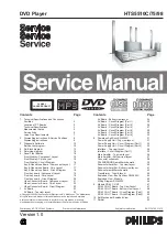
Published by KC-TE 0519 AV Systems
Printed in the Netherlands
Subject to modifi cation
EN 3139 785 31570
HTS5510C/75/98
DVD Player
CLASS 1
LASER PRODUCT
1 Technical
Specifi cations and Connection
Facilities
2
Location of PC Boards
2
Technical
Specifi cations
3
Measurement
Setup
4
Service
Aids
5
Lead Free Requirements
7
2
Dismantling instructions & Service Positions
8
Dismantling
instructions
8
3 Diagnostic
Software
10
Service test program
10
4
Set Block diagram
13
5
Set wiring diagram
14
6 Panel
Front
Boards
15
Front Display - Component Layout
15
Front Display - Chip Layout
15
Front Display - Circuit Diagram
16
Key & Open/close Board - Component Layout
17
Key & Open/close Board - Chip Layout
17
Key & Open/close Board - Circuit Diagram
18
Front key board - Component Layout
19
Front key board - Chip Layout
19
Front key board - Circuit Diagram
20
Video Connector Board - Component Layout
21
Video Connector Board - Chip Layout
22
Video Connector Board - Circuit Diagram
22
7 AV
Board
23
AV Board - Top view layout
23
©Copyright 2005 Philips Consumer Electronics B.V. Eindhoven, The Netherlands.
All rights reserved. No part of this publication may be reproduced, stored in
a retrieval system or transmitted, in any form or by any means, electronic,
mechanical, photocopying, or otherwise without the prior permission of Philips.
Version 1.0
Contents Page
Contents Page
AV Board - Bottom view layout
24
AV Board - Circuit Diagram (Part 1)
25
AV Board - Circuit Diagram (Part 2)
26
AV Board - Circuit Diagram (Part 3)
27
AV Board - Circuit Diagram (Part 4)
28
AV Board - Circuit Diagram (Part 5)
29
AV Board - Circuit Diagram (Part 6)
30
8
Powerbox Spk Assy SW5500C
31
Power Supply Unit - Top view layout
31
Power Supply Unit - Circuit Diagram (Part 1)
32
Power Supply Unit - Circuit Diagram (Part 2)
33
Interface - Top view layout
34
Interface - Circuit Diagram (Part 1)
35
Main Amplifer - Top view layout
36
Main Amplifer - Bottom view layout
37
Connector
schematic
38
FR+SURROUND
amplifi er schematic
39
Subwoofer Amplifer - Top view layout
40
Subwoofer Amplifer - Bottom view layout
41
Subwoofer
amplifi er schematic
42
Transformer - Top silk layout
43
Exploded View - Box Spk Assy SW5500C
44
Exploded View - Module
45
Wiring Diagram SW5500C
46
9
Module SD6.3 CH HT
47
SD6.3 CH HT Board - Top View Layout
47
SD6.3 CH HT Board - Bottom View Layout
48
SD6.3 CH HT Board - Circuit Diagram (Part1)
49
SD6.3 CH HT Board - Circuit Diagram (Part2)
50
10 Set Mechanical Exploded View
51
11 Partlist
53
Summary of Contents for HTS5510C/75
Page 12: ...EN 12 HTS5510C 75 98 3 Diagnostic Software Notes ...
Page 23: ...EN 23 HTS5510C 75 98 AV Board 7 AV Board AV Board Top view layout 7 ...
Page 24: ...EN 24 HTS5510C 75 98 AV Board Bottom view layout AV Board 7 ...
Page 34: ...EN 34 HTS5510C 75 98 Interface Top view layout Powerbox Spk Assy SW5500C 8 ...
Page 36: ...EN 36 HTS5510C 75 98 Main Amplifer Top view layout Powerbox Spk Assy SW5500C 8 ...
Page 37: ...EN 37 HTS5510C 75 98 Main Amplifer Bottom view layout Powerbox Spk Assy SW5500C 8 ...
Page 40: ...EN 40 HTS5510C 75 98 Subwoofer Amplifer Top view layout Powerbox Spk Assy SW5500C 8 ...
Page 41: ...EN 41 HTS5510C 75 98 Subwoofer Amplifer Bottom view layout Powerbox Spk Assy SW5500C 8 ...
Page 43: ...EN 43 HTS5510C 75 98 Transformer Top silk layout Powerbox Spk Assy SW5500C 8 ...
Page 44: ...EN 44 HTS5510C 75 98 Exploded View Box Spk Assy SW5500C Powerbox Spk Assy SW5500C 8 ...
Page 45: ...EN 45 HTS5510C 75 98 Exploded View Module Powerbox Spk Assy SW5500C 8 ...
Page 51: ...EN 51 HTS5510C 75 98 10 Set Mechanical Exploded View Set Mechanical Exploded View 10 ...
Page 52: ...EN 52 HTS5510C 75 98 Set Mechanical Exploded View 10 Notes ...


