background image

7-3

2. Installation

1. Using desoldering braid, remove the solder from 

the foil of each pin of the flat pack-IC on the CBA 
so you can install a replacement flat pack-IC more 
easily.

2. The “ ” mark on the flat pack-IC indicates pin 1. 

(See Fig. S-1-7.) Be sure this mark matches the 1 
on the PCB when positioning for installation. Then 
presolder the four corners of the flat pack-IC. (See 
Fig. S-1-8.)

3. Solder all pins of the flat pack-IC. Be sure that 

none of the pins have solder bridges.

Instructions for Handling Semi-

Special Information BGA IC & Flat Pack-IC

conductors

Electrostatic breakdown of the semi-conductors may 
occur due to a potential difference caused by 
electrostatic charge during unpacking or repair work.

1. Ground for Human Body

Be sure to wear a grounding band (1 M

) that is 

properly grounded to remove any static electricity that 
may be charged on the body.

2. Ground for Workbench

Be sure to place a conductive sheet or copper plate 
with proper grounding (1 M

) on the workbench or 

other surface, where the semi-conductors are to be 
placed. Because the static electricity charge on 
clothing will not escape through the body grounding 
band, be careful to avoid contacting semi-conductors 
with your clothing.

Example :

Pin 1 of the Flat Pack-IC
is indicated by a "    " mark.

Fig. S-1-7

Presolder

CBA

Flat Pack-IC

Fig. S-1-8

<Incorrect>

CBA

Grounding Band

Conductive Sheet or
Copper Plate

1M

1M

<Correct>

CBA

Summary of Contents for HTS3220

Page 1: ... 8 1 to 8 5 10 Cabinet Disassembly Instructions 9 1 to 9 2 16 Main Unit Touch Board 11 Troubleshooting 10 1 12 Software Upgrading Procedure 11 1 13 Software Version Check 11 2 14 Block Diagram 12 1 15 Wiring Diagram 13 1 17 Main Unit VFD Display Board PT6311 IC Specification 15 2 18 Main Unit iPOD Terminal Door Control and USB Board Layout Diagram 16 1 20 Main Unit Decoder Board 19 Main Unit AMP B...

Page 2: ... Video Output Connectors S N video unweighted at 75Ω 71dB Singal To Noise Ratio 50dB Typical 3 minutes Search Tuning Sensitivity 19 35 dBf Search Time Digital Tuning System Maximun tuning error of a recalled program 22 5 kHz Maximun tuning error during operation drift 50 kHz Stop level vision carrier 31dBμV RF Signal 2 5min Modulation 1kHz Noise Limlited sensitivity 26dB Mono 22 dBf Noise Limlited...

Page 3: ...torage Class Type of connector Class support UMS USB Mass File System FAT12 FAT24 FAT36 Series A Connector 1 5 3 HDMI Output 1 5 4 Sampling Frequency Compatibility MP3 32kHz 44 1kHz 48kHz WMA 44 1kHz 48kHz 1 5 4 Canstant bit rate PHILIPS specified using iPod iPhone MP3 112 kbps 320 kbps WMA 44 kbps 192 kbps HDMI version 1 3 Type of connector Type A connector 19 pins 1 7 Video Performance 1 7 1 SNR...

Page 4: ... DVD R RW DVD Video Video CD SVCD DVD R DL DVD R DL USB flash drive x 2 Compression Formats MPEG2 MPEG1 DivX 3 11 DivX 4 x DivX 5 x DivX 6 0 MPEG4 x Audio Playback 1 Playback Media Audio CD CD R RW DVD R DL DVD R RW DVD R RW MP3 CD MP3 DVD USB flash drive WMA CD x 2 Compression Format Do by Digital MP3 MPEG2 Multichannel PCM WMA x 3 MPEG1 bit rates 64 384 kbps and VBR x Still Picture Playback 1 Play...

Page 5: ...the pickup lens when the diode is turned on Do not look directly at the laser beam CAUTION Use of controls and adjustments or doing procedures other than those specified herein may result in hazardous radiation exposure Location Inside Top of DVDmechanism Do not look directly at the laser beam coming from the pickup or allow it to strike against your skin Drive Mechanism Assembly Laser Beam Radiat...

Page 6: ...partment if you are not using the product for an extended period of time Only use microfiber cloth to clean the product Important Important Safety Precautions Read and understand all instructions before you use your home theater If damage is caused by failure to follow instructions the warranty does not apply Safety Riskof electricshockor fire Never expose the product and accessories to rain or wat...

Page 7: ... in the language of your choice Disposal of your old product and batteries Your product is designed and manufactured with high quality materials and components which can be recycled and reused When this crossed out wheeled bin symbol is attached to a product it means that the product is covered by the European Directive 2002 96 EC Please inform yourself about the local separate collection system f...

Page 8: ... and externally exposed accessible parts RF terminals antenna terminals video and audio input and output terminals microphone jacks earphone jacks etc is lower than or equal to the specified value in the table below Measuring Method Power ON Insert load Z between B earth ground power cord plug prongs and exposed accessible parts Use an AC voltmeter to measure across the terminals of load Z See Fig...

Page 9: ...discharges ESD Careless handling during repair can reduce life drastically Make sure that during repair you are at the same potential as the mass of the set by a wristband with resistance Keep components and tools at this same potential Available ESD protection equipment Complete kit ESD3 small tablemat wristband connection box extension cable and earth cable 4822 310 10671 Wristband tester 4822 3...

Page 10: ... defective loader 4 Put a paper clip on the flexfoil to short circuit the contacts fig 1 5 Replace the defective loader with a new loader 6 Remove paperclip from the flexfoil and connect it to the new loader 7 Remove solder joint on the ESD protection point ATTENTION The laser diode of this loader is protected against ESD by a solder joint which shortcircuits the laserdiode to ground For proper funct...

Page 11: ...SAC305 with order code 0622 149 00106 If lead free solder paste is required please contact the manufacturer of your solder equipment In general use of solder paste within workshops should be avoided because paste is not easy to store and to handle Use only adequate solder tools applicable for lead free solder alloy The solder tool must be able To reach at least a solder temperature of 400 C To sta...

Page 12: ... sets You will find this and more technical information within the magazine chapter workshop news For additional questions please contact your local repair helpdesk How to Remove Install Flat Pack IC Special Information of BGA IC Flat Pack IC 1 Removal With Hot Air Flat Pack IC Desoldering Machine 1 Prepare the hot air flat pack IC desoldering machine then apply hot air to the Flat Pack IC about 5...

Page 13: ...ux which is applied to all pins of the flat pack IC you can remove it easily Fig S 1 3 2 Affix the wire to a workbench or solid mounting point as shown in Fig S 1 5 3 While heating the pins using a fine tip soldering iron or hot air blower pull up the wire as the solder melts so as to lift the IC leads from the CBA contact pads as shown in Fig S 1 5 4 Bottom of the flat pack IC is fixed with glue ...

Page 14: ...ductors may occur due to a potential difference caused by electrostatic charge during unpacking or repair work 1 Ground for Human Body Be sure to wear a grounding band 1 MΩ that is properly grounded to remove any static electricity that may be charged on the body 2 Ground for Workbench Be sure to place a conductive sheet or copper plate with proper grounding 1 MΩ on the workbench or other surface ...

Page 15: ...andby b OPEN CLOSE Opens or closes the disc compartment m a b c d e f g h i j k l n q r s t p o Your home theater Congratulations on your purchase and welcome to Philips To fully benefit from the support that Philips offers register your home theater at www philips com welcome Main unit a Display panel b Increases or decreases volume c SOURCE Selects an audio video source for the home theater d St...

Page 16: ...ckward or fast forward In radio mode press left or right to search a radio station press up or down to fine tune a radio frequency f INFO Displays information about what is playing g Playback buttons Control playback h TREBLE BASS Changes treble or bass Use with i Numeric buttons Selects an item to play j AUDIO SYNC Selects an audio language or channel Press and hold to synchronize audio with vide...

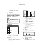
Page 17: ...t o t t c e n n o C TO SUBWOOFER connector on the main unit e m o h r u o y t c e n n o C theater r e t a e h t e m o h r u o y t c e n n o c u o y s p l e h n o i t c e s s i h T to aTV and other devices The basic connections of the home theater with its accessories are provided in the Quick Start For a comprehensive interactive guide see www connectivityguide philips com e t o N m o t t o b r o ...

Page 18: ...Option 1 Connect audio through analog audio cables Cable not supplied TV TV Connect to the TV Connect your home theater directly to a TV through one of the following connectors from highest to basic quality video a HDMI b Scart c Composite video Option 1 Connect to the TV through HDMI Note If the HDTV has a DVI connector connect using an HDMI DVI adapter If the TV supports EasyLink HDMI CEC contro...

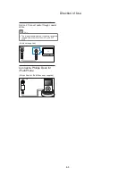
Page 19: ... audio through coaxial cable Note The digital coaxial cable or connector might be labeledCOAXIAL DIGITAL OUT or SPDIF OUT Cable not supplied Connect a Philips Dock for iPod iPhone Philips Dock for iPod iPhone not supplied TV DOCK for iPod ...

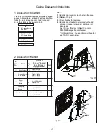
Page 20: ...d or desoldered Axx Screw CNxx Jxx CONxx Connector D3 5X12BA is specification of screw Unhook Unlock Release Unplug or Desolder e g 7 A01 seven Screws ID Loc No Part Removal Fig No Remove Unhook Unlock Release Unplug Desolder Note 3 DVD Loader Driver VFD Display Board DVD Loader Driver VFD Display Board 4 USB Board Ipod Docking Board USB Board Ipod Docking Board 5 DVD Door DVD Door 2 Decoder Board...

Page 21: ...9 2 Fig D3 Fig D4 Fig D5 Cabinet Disassembly Instructions A10 A09 A09 A02 A02 A03 A03 ...

Page 22: ...rm the speaker Check the 1st pin which location is U1 if it has DC 27V input Check the 2en pin which location is U8 PT2313 if it has DC 9V Check the 2en pin which location is U8 if it has DC 9 1V Check the D10 diode whether has DC 9 1V Yes Check the 4th pin which location is U1 and U3 on the AMP Board wether has MUTE signal input Yes Check the U15 wether has DC 3 3V Yes Check the Cable CON2 and CO...

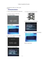
Page 23: ...upport A Connect to TV and Turn on Main Unit C Press the OK on the Remote Control D Software Upgrading TV Screen Display E After 1 or 2 minute TV Screen will reset and Display Software Upgrade finish Main unit Screen Display Main unit Screen Display TV Screen Display B When insert the USB Device with software Meanwhile the TV Screen Display 11 1 USB and ...

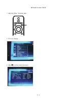
Page 24: ...Software Version Check 1 Select the Menu like below show 2 TV Screen Display 2 Select to get the Version information 11 2 ...

Page 25: ...FM L R COAXIAL SPDIF_COAXIAL HPD CEC_OUT CEC_IN IPOD UART MCU5V SW IN 1 2 3 5 TOVFD 2 0 5P GND CLK DATA STB IR WT5700 BPF BASS 1 2 3 MCU5V SDA SCL GND AUTO MUTE S MUTE MCU5V GND 27V VFD1 28V M5V M3 3V SW IN FL IN FR IN VFD2 M1 8V GND GND AGND 1 2 3 4 O MPEG 2 0 4P 1 2 3 5 TO VFD 2 0 5P 1 2 3 5 6 O MPE G 2 5 6P Q 90 4 S MUTE I2C MAIN POD_UART MUTE ECO POWER MUTE Q 9014 R 4 7K POW MUTE R 1K R 2 2K G...

Page 26: ...EMOTE ADD2 MUTE MCU5V 27V_IN S_MUTE GND ECO POWER ROUT GND SW_IN GND LOUT GND IPOD TX IPOD RX NC IPOD_5V IPOD_IN_R IPOD_IN_L GND GND 5V GND GND GND 5V USBM USBP GND P4 SL SL GND LIMIT SP SP J3 MCU5V GND 27V VFD1 VFD2 ADD2 GND VCC SWIN GND ROUT ROUT LOUT GND ROUT GND ECO_POWER MUTE SMUTTE MCU5V 27V_IN wire8 wire7 wire1 wire2 wire3 wire4 Sub015 wire5 wire6 CON1 CON4 110 220V Power Control Board for ...

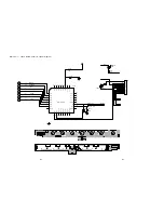
Page 27: ... LED201 LED R204 220 PWM LED VDD OUT 4 22 OUT 6 16 SI 2 30 SCL 19 SI 1 29 PWMO 1 17 SI 0 28 OUT 0 26 OUT 1 25 OUT 2 24 OUT 3 23 PWMO 0 20 TESET 8 SI 7 3 SI 8 4 SI 9 5 SI 4 32 OUT 7 15 OUT 8 14 VSS 10 OUT 10 12 OUT 11 11 INT 9 SDA 18 OUT 5 21 SI 6 2 SI 5 1 SI 11 7 SI 10 6 OUT 9 13 SI 3 31 VDD 27 U201 WT5701 UG321 OPEN STOP PLAY POWER SOURCE VOL VOL Main Unit Touch Board Circuit Layout Diagram 14 1 ...

Page 28: ...S6 S7 S8 S9 27V DC5V C104 104 VF1 VF2 REM 1 GND 2 Vcc 3 S100 REMOTE REMOTE DC5V S10 S11 S12 S13 S14 S15 G1 G2 G3 G4 G5 G6 G7 G8 C105 47uF 16V S1 S2 S3 S4 S5 S6 S7 G1 G2 G3 G4 G5 G6 G7 G8 S9 S10 S11 S12 S13 S14 S8 S15 R100 6 81 2W R101 6 81 2W R115 47 C110 47uF 25V C111 104 LED VF1 1 VF1 2 VF2 31 VF2 32 NC 4 S15 5 S14 6 NC 7 S13 8 S12 9 S11 10 S10 11 S9 12 S8 13 S7 14 S6 15 S5 16 S4 17 S3 18 S2 19 ...

Page 29: ... Circuit Current I sc Vin Vo k p A 0 5 V 5 Input Voltage Range Vin 0 1 Io V A 0 2 o 4 38 V Output Voltage Tolerance Vo Over Vin Range I o 2 0 A 1 0 2 0 Vo T a 0 C to 60 C Line Regulation Regline Over Vin V 5 0 5 2 0 e g n a r o Load Regulation Regload 0 1 Io V 5 0 5 2 0 A 0 2 o Vo Ripple Noise Vn Vin Vin min Io V 2 A 0 2 o Transient Response ttr 0 0 2 0 0 1 e g n a h c d a o l 0 5 µSec with Co 100...

Page 30: ...Main Unit VFD Display Board Layout Diagram 15 3 15 3 ...

Page 31: ...9 IPOD 9P 1 5V 2 NC 3 RX 4 GND D 5 AL 6 TX 7 GND A 8 AL 9 GND 1 2 3 4 CN401 vbus 1 D 2 D 3 GND 4 Shield 5 GND 6 J401 USB GND u D D vbus 4P Main Unit iPod Terminal Door Control and USB Board Circuit Layout Diagam 16 1 16 1 SW301 1 2 CN301 2P 35 HTS3220 03A1 Touch Switch ...

Page 32: ... 2N3904 2 1 3 TP26 CE29 CD263 470UF16V D8H12 C30 0 1uF R54 4 7K J5 CON2 54 2 1 2 CE27 CD263 100UF35V D8H7 CE34 220uF 35V R58 2 2K R50 4 7K L13 FB 1206 D1 SK34 1 2 J3 CON2 54 2 1 2 R55 1M R47 4 7K U9 BZ1 1 2 3 4 5 6 7 8 9 1 2 3 4 5 6 7 8 9 TP21 D5 27V CB12 0 1uF D4 FR104 1 2 Q4 D965 DIP 3 1 2 CE35 CD11 220UF35V D8H12 Q5 2N3904 2 1 3 R62 330 TP28 R46 4 7K C29 0 047uF di un R51 47K D6 1N4001 1 2 Q6 D...

Page 33: ...805 C26 470pF H5 HOLE GND 2 3 4 5 9 8 7 6 1 2 3 4 5 9 8 7 6 1 L2 33UH 3 5A LHP1014 CE11 2 2UF16V 0603 R11 10K NC R32 4 7K C10 470pF TP11 R22 6 8K CE14 1uF R23 24k P1 PRC 101A 3 2 1 4 5 6 CE6 47UF C9 470pF L6 FB DIP CE10 1uF D9 1N60 1 2 D7 1N60 1 2 Y2 C2 0 47uF dilun CE22 1uF CE23 CHIP CAP EL 100UF 35V M 8 7 CE19 CD11X 4 7UF16V D4H7 CE2 2 2UF16V 0603 C8 1800pF R3 100K CE20 1uF U3 23 1 2 3 4 5 6 7 8...

Page 34: ...not internally connected to PVCCR or AVCC LOUT 22 O Class D 1 2 H bridge positive output for left channel PGNDL 23 24 P Power ground for left channel H bridge VCLAMP 11 P Internally generated voltage supply for bootstrap capacitors BSR 16 I O Bootstrap I O for right channel ROUT 15 O Class D 1 2 H bridge negative output for right channel PGNDR 13 14 P Power ground for right channel H bridge PVCCR ...

Page 35: ...Main Unit AMP Board Layout Diagram 17 4 17 4 ...

Page 36: ...CB97 0 1uF Q17 2N3904 2 1 3 C113 150pF R239 150K R226 4 7 C112 2200pF R220 10K CON3 H24 SMD0 5 25 26 3 4 6 7 8 9 10 11 12 13 14 15 16 17 18 19 20 21 22 23 24 2 5 1 CB94 0 1uF NC Q22 2N3906 2 1 3 C111 150pF TP48 R233 680K Q23 8550 DIP 2 1 3 Q20 8550 DIP 2 1 3 R217 10K CB92 0 1uF R241 10K R215 10K CB91 0 1uF R222 100 R227 10K R231 1 0805 R234 10K CB96 0 1uF R237 20K TP70 CE50 220UF 10V R219 33 R240 ...

Page 37: ...O TROPENPWM PWMOUT1 _ADIN0 TRO FOO AGND18_DMPLL AVDD18_DMPLL USB_DP USB_DM VDD33_USB VSS33_USB PAD_VRT VDD18_USB VSS18_USB USB_XTALO GPIO15 USB_XTALI GPIO14 FG GPIO16 IOA22 GPIO18 DVDD18 IOA2 IOA3 IOA4 IOA5 IOA6 IOA7 HIGHA0 IOA18 IOA19 DVDD33 IOWR A16 HIGHA7 HIGHA6 HIGHA5 HIGHA4 HIGHA3 HIGHA2 HIGHA1 IOA20 IOCS IOA1 IOOE AD0 AD1 DVSS18 AD2 AD3 AD4 AD5 AD6 IOA21 GPIO17 ALE AD7 DVSS33 A17 IOA0 DVDD18...

Page 38: ...35 10UF 10V 0805 U10 K4S641632H UC60 1 2 4 12 5 7 9 8 10 46 11 13 15 16 17 18 19 35 22 23 24 25 26 14 41 29 30 31 32 33 34 36 37 38 39 40 43 42 44 52 45 47 49 48 50 51 53 54 20 21 3 6 27 28 VCC DQ0 DQ1 VSSQ DQ2 DQ3 VCCQ DQ4 DQ5 VSSQ DQ6 DQ7 DQML WE CAS RAS CS A11 A10 AP A0 A1 A2 A3 VCC VSS A4 A5 A6 A7 A8 A9 NC CKE CLK DQMH NC VCCQ DQ8 DQ9 VSSQ DQ10 DQ11 VCCQ DQ12 DQ13 DQ14 DQ15 VSS BA0 A13 BA1 A12...

Page 39: ... H L H VHH AB INB DB INB DB INB DQ8 DQ14 High Z DQ15 A 1 CMOS Standby VccB 0 3V X X VccB 0 3V H X High Z High Z High Z TTL Standby H X X H H X High Z High Z High Z Output Disable L H H H L H X High Z High Z High Z Hardware Reset X X X L L H X High Z High Z High Z Sector Group Protect L H L VB IDB L H SA A6 L A1 H A0 L Note 2 X X Sector Unprotect L H L VB IDB Note 1 SA A6 H A1 H A0 L Note 2 X X Tem...

Page 40: ... TXC 2 TXC 2 HDMI_HPD 5 TS_DATA2 2 CECOUT 5 DV33 1 2 3 5 89S_3V3 2 5 VCC 1 2 5 GND 1 2 3 5 VCC DV33 VCC 89S_3V3 D22 NC D21 NC R164 1 5K R161 NC 27K R166 0 D23 NC R162 47 NC CB38 0 1uF NC D16 NC P3 HDM2MB 19 B 1 2 3 4 5 6 7 8 9 10 11 12 13 14 15 16 17 18 19 22 21 20 23 Q11 CES2312 NC 1 3 2 D17 NC D12 NC CE33 10uF 25V D13 NC D14 NC CB37 0 1uF D24 IN4148 D20 NC IN4148 D15 NC R160 0 R165 0 L37 FB 600 ...

Page 41: ...5 13 16 17 18 19 20 21 22 23 30 31 32 33 34 35 36 37 38 39 43 44 45 46 47 48 49 50 51 52 11 24 29 42 12 14 25 26 28 27 41 40 NC SCLK DVD_ON SSDA MODE XCIAN XCOUT RST XOUT VSS OPEN_SW M_OPEN CLOSE_SW VFD_CLK VFD_DATA VFD_STB REMOTE ROTB2 ROTA2 TX1 DAB_SW STANDBY MUTE_MCU MUTE_LINE LED_CTRL ECO_POWER MSDA MSCL AD0 NC AD3 AD_VREF TREO IPOD_SW SD_DET AD4 AD5 AD6 USB_DET DVD_SW XIN RX1 TX2 ROTA3 AD2 VC...

Page 42: ...4 5 9 8 7 6 1 TP5 TP75 CE69 220UF 10V R375 47K TP8 TP9 Q1 2N3904 2 1 3 CE71 CD11X 220UF16V D6 3H7 R284 330 P1 CON2 0 5 红色 3 2 1 4 5 J5 CON2 0 5 1 2 3 4 5 TP8 TP82 TP11 TP88 J3 CON2 0 7 1 2 3 4 5 6 7 R374 2K TP8 CE66 CD11X 100UF35V D8H7 R373 20K TP14 TP72 TP87 TP12 H4 HOLE GND 2 3 4 5 9 8 7 6 1 2 3 4 5 9 8 7 6 1 TP76 增加 MP3 IN L MP3_IN_R M CLOSE M_OPEN M M MCU_HPD 89S_HPD HDMI_HPD LOUT ROUT 27V FAN...

Page 43: ...de selection input 0 for static mode or microcontroller mode grounded for I2C bus MODE1 18 bpts5tht5v mode selection input 1 for static mode or AO address input and output for microcontroller mode MODE2 19 bpts5tht5v mode selection input 2 for static mode or U_RDY output for microcontroller mode SEL_STATIC 20 apio selection input for static mode I2C bus mode or L3 bus mode SLICER_SEL0 21 bpts5tht5...

Page 44: ...Main Unit Decoder Board Layout Diagram 18 9 18 9 ...

Page 45: ...Subwoofer AMP Power Board Circuit Diagram 19 1 19 1 ...

Page 46: ...Subwoofer AMP Power Board Circuit Diagram 19 2 19 2 IC5 TDA8920CJ ...

Page 47: ...g input IN1 8 positive audio input for channel 1 IN1 9 negative audio input for channel 1 VDDA1 10 positive analog supply voltage for channel 1 SGND1 11 signal ground for channel 1 VSSA1 12 negative analog supply voltage for channel 1 PROT 13 time constant capacitor for protection delay VDDP1 14 positive power supply for channel 1 BOOT1 15 bootstrap capacitor for channel 1 OUT1 16 PWM output from ...

Page 48: ...Subwoofer AMP Power Board Layout Diagram 19 4 19 4 ...

Page 49: ...Main Unit Exploded View 20 1 20 1 ...

Page 50: ...Subwoofer Exploded View 20 2 20 2 SUB016 For 98version ...

Page 51: ...Packing Exploded View 20 3 20 3 SPKL SPKR ACC12 A ACC12 C ACC15 ACC8 ACC9 ACC10 ACC11 SUB001 ACC12 D ACC12 B ACC1 ACC5 ACC2 ACC3 ACC4 ACC15 Main Unit ACC16 ACC12 E ACC13 ACC14 ACC12 F ACC12 G ...

Page 52: ...Revision List Revision List Version 1 0 Initial Release 21 1 ...

Reviews: