Great user manuals database on
UserManuals.info
Main Board Print-Layout (Bottom Side) for DVP3156/XX, DVP3166
(
K
)
/XX
6-21
Page 1: ...785 32471 Version 1 1 DVP3156 DVP3160Kˈ DVP3166 K Service Manual PHILIPS GB Copyright 2007 Philips Consumer Electronics B V Eindhoven The Netherlands All rights reserved No part of this publication may be reproduced stored in aretrieval system or transmitted in any form or by any means electronic mechanical photocopying or otherwise without the prior permission of Philips CLASS 1 LASER PRODUCT Pub...
Page 2: ...able bit rate fs 32 44 1 48 kHz Analogue Sound Stereo Dolby surround compatible downmix from Dolby Digital multi channel sound Audio performance DA converter 24bits 192KHz DVD fs 96kHz 4Hz 44kHz fs 48kHz 4Hz 22kHz SVCD fs 48kHz 4Hz 22kHz fs 44 1kHz 4Hz 20kHz CD VCD fs 44 1kHz 4Hz 20kHz Signal Noise 1kHz 90dB Dynamic Range 1kHz 80dB Cross talk 1kHz 70dB Distortion Noise 1kHz 65dB MPEG MP3 MPEG Audi...
Page 3: ...mains cord and connect a wire between the two pins of the mains plug 2 Set the mains switch the on position keep the mains cord unplug 3 Measure the resistance value between the mains plug and the front panel controls and chassis bottom 4 Repair or correct unit when the resistance measurement is less than 1M 5 Verify this before you return the unit to the customer user ref UL standard no 1492 6 Sw...
Page 4: ...ff It is possible to touch copper tracks and or components in this unshielded primary area when you service the player Service personnel must take precautions to prevent touching this area or components in this area A lighting stroke and a stripe marked printing on the printed wiring board indicate the primary side of the power supply Never replace modules or components while the unit is on 2 Lase...
Page 5: ...id wear out of tips switch off un used equipment or reduce heat x Mix of lead free solder alloy parts with leaded solder alloy parts is possible but PHILIPS recommends strongly to avoid mixed solder alloy types leaded and lead free If one cannot avoid clean carefully the solder joint from old solder alloy and re solder with new solder alloy SAC305 x Use only original spare parts listed in the Serv...
Page 6: ...rews around the Top Cover then remove the Top Cover Figure 1 Step2 If it is necessary to dismantle Loader or Front Panel It should be remove the Front door assembly first Figure 2 Note Make sure to operate gently otherwise the guider would be damaged 2 1 Figure 1 Figure 2 Please kindly note that dismantle the front door assembly carefully to avoid damage tray and the front door assembly ...
Page 7: ...it through the instruction as below Figure 3 Note Make sure to operate gently otherwise the guider would be damaged Step4 Dismantling Loader disconnect the 3 connectors aiming in the below figure and remove 1 screw around the Loader Figure 4 Push the guider until the tray out Make sure to operate gently to avoid damage happening Figure 3 CON 1 CON 2 CON 3 Figure 4 2 2 ...
Page 8: ...ctions Dismantling Instruction Step5 Dismantling Front Panel disconnect the 3 connector then release the snaps on the both sides of Front Panel and bottom cabinet then gently pull the Panel out from the set Figure 5 6 7 Snap 1 Figure 6 Snap 2 Figure 7 Figure 5 CON 4 CON 6 CON 5 2 3 ...
Page 9: ...cal and Dismantling Instructions Dismantling Instruction Step6 Dismantling Main Board first disconnect the connector and then remove 4 screws Figure 8 Step7 Remove the 2 screws on Power Board to dismantle the Power Board Figure 9 2 4 Figure 9 Figure 8 CON 8 ...
Page 10: ...y TO START 3 Press OK button to confirm then screen will display Files coping UPGRADING 4 The upgraded disc will automatically out when files coping complete then take out the disc 5 About 1 minute later the trace will automatically close when upgrading complete B Read out the software versions to confirm upgrading 1 Power on the set and press Setup button on the remote control 2 Press 1 3 7 9 but...
Page 11: ...OO signals 2 If there are F F T and T signals output from U3 Check Replace the loader Yes Yes No Go Check whether laser voltage 2V for VCD 2 2V for DVD on Collector of Q6 and Q5 Check the FFC connection between 24P and the loader 1 Whether voltage on pin 112 of U2 varies between 0 and 3 3V 3 3V for VCD and 0V for DVD 2 Whether peripheral components are eroded or badly soldered Trouble shooting cha...
Page 12: ...supply on the power board is normal Check Correct connection Whether the connection to K301 is broken Correct the connection Replace U2 No No Yes Yes Check if the CON301 on the front board to CN5 on the decoder board is in good contact Whether there is 0V and 3 3V voltage difference on Pin 104 PCON of U2 Trouble shooting chart Remark Trouble shooting chart for DVP3160K XX ...
Page 13: ...eck whether U2 are eroded All output voltages on the power board is 0V or deviated Check whether there is 300V on C4 Check whether 100KHz oscillating signal on Pin6 of U1 Check if 5V 12V 12V and are short Check whether the components in the short circuit voltage are defected or eroded Yes Yes Yes Yes U1 PIN 3 RC waveform Check whether F1 is blown Trouble shooting chart Remark Trouble shooting char...
Page 14: ...FC connection between 24P and the loader Check U2 and peripheral components Re solder or replace the defective parts Check the connection between U2 Correct connection Replace U2 or loader Yes Check whether there is laser voltage 2V for VCD and 2 2V for DVD on Collector of Q6 Q5 Check if there is RFO signal on pin17 of CN2 The normal RFO signal is a clear reticulated wave CheckU2 U3 andperipheral ...
Page 15: ...ents Check whether there is voltage variance on pin 23 of U2 check if bad solder exist on U2 and peripheral components Replace the bad spare parts Check Q2 Q3 Q4 whether in good condition Yes Yes Yes Go Correct connection Change U2 or the loader No No Yes Check laser voltage 2V output on Collector of Q6 if pin 23 of U2 is at low level No Trouble shooting chart Remark Trouble shooting chart for DVP...
Page 16: ...the U2 s pin 97ˈ98ˈ100 arrive the CN5 connect condition Correct connection Replace U301 or LED Yes Yes Yes No Check VCC 5v voltage on the power and front board Check there are CS DATA and CLK signals on CON301 on the front board 1 Check whether bad solder exists on U301 and pins of LED 2 Check whether the circuit connected to K302 K303 K304 and K301 is broken 3 Check whether R300 R301 and R302 are...
Page 17: ...nsistor Q26 Q30 Q31 are normal Checking the U10 leads have not been broken or open Correct connection Replace U2 if the clock signal ACLK ABCK and ALRCK output by U2 are normal Check whether the U2 or U10 power supply normal No Yes Check the power supply voltages 12V and 12V to the operation amplifying Q15 IS normal Yes Check U10 Replace U2 or U10 No Yes SACLK waveform SBCLK waveform SSLRCK wavefo...
Page 18: ...V power supply voltages on the decoder board are normal Check Y1 R15 R217 C17 and C18 Check other of power supply electric circuit Correct the connection Check whether the video filter network circuit is normal Yes Yes No No No Check whether the 27MHz output signal is Change U2 Yes Trouble shooting chart Remark Trouble shooting chart for DVP3160K XX ...
Page 19: ...oscope to check if there is output waveform from the first pin IR of the remote censor after pressing button on the remote control Check the PIN 11 RC waveform of IC1 on the remote PCB Check if there is IR signal on pin 109 of U2 Check if the power supply voltage to the remote censor is normal are normal Go No No No Yes Yes Yes Correct connection Yes Change U2 IR waveform Trouble shooting chart Re...
Page 20: ...ignal output Check the loaded circuit Crystal oscillator Y1 and peripheral components are defected or eroded Check whether short circuit or bad solder on U7 Check if short circuit and bad solder exist on Pin Y1 No No No No No Yes Yes Yes Yes Yes Reconnect the component in short circuit Check U2 Yes No 27M waveform SDRAM R59 SDCLK waveform Check whether all the voltages from the power board to the ...
Page 21: ...nals 2 If there are F F T and T signals output from U3 Check Replace the loader Yes Yes No Go Check whether laser voltage 2V for VCD 2 2V for DVD on Collector of Q6 and Q5 Check the FFC connection between 24P and the loader 1 Whether voltage on pin 112 of U2 varies between 0 and 3 3V 3 3V for VCD and 0V for DVD 2 Whether peripheral components are eroded or badly soldered Motor no move Trouble shoo...
Page 22: ... on the power board is normal Check Correct connection Whether the connection to K301 is broken Correct the connection Replace U2 No No Yes Yes Check if the CON301 on the front board to CN5 on the decoder board is in good contact Whether there is 0V and 3 3V voltage difference on Pin 104 PCON of U2 Trouble shooting chart Remark Trouble shooting chart for DVP3156 XX DVP3166 K XX ...
Page 23: ...hether U2 are eroded All output voltages on the power board is 0V or deviated Check whether there is 300V on C4 Check whether 100KHz oscillating signal on Pin6 of U1 Check if 5V 12V 12V and are short Check whether the components in the short circuit voltage are defected or eroded Yes Yes Yes Yes U1 PIN 3 RC waveform Check whether F1 is blown Trouble shooting chart Remark Trouble shooting chart for...
Page 24: ...nection between 24P and the loader Check U2 and peripheral components Re solder or replace the defective parts Check the connection between U2 Correct connection Replace U2 or loader Yes Check whether there is laser voltage 2V for VCD and 2 2V for DVD on Collector of Q6 Q5 Check if there is RFO signal on pin17 of CN2 The normal RFO signal is a clear reticulated wave Check U2 U3 andperipheral compo...
Page 25: ...Check whether there is voltage variance on pin 23 of U2 check if bad solder exist on U2 and peripheral components Replace the bad spare parts Check whether pin 1 to pin38 of U2 and peripheral components are badly soldered defected Check Q2 Q3 Q4 whether in good condition Yes Yes Yes Go Correct connection Change U2 or the loader No No Yes Check laser voltage 2V output on Collector of Q6 if pin 23 o...
Page 26: ... s pin 97ˈ98ˈ100 arrive the CN5 connect condition Correct connection Replace U301 or LED Yes Yes Yes No Check VCC 5v voltage on the power and front board Check there are CS DATA and CLK signals on CON301 on the front board 1 Check whether bad solder exists on U301 and pins of LED 2 Check whether the circuit connected to K302 K303 K304 and K301 is broken 3 Check whether R300 R301 and R302 are open ...
Page 27: ... Q26 Q30 Q31 are normal Checking the U10ˈU27ˈ U28 leads have not been broken or open Correct connection Replace U2 Check whether the U2 or U10 ˈ U27 ˈ U28 power supply normal No Yes Check the power supply voltages 12V and 12V to the operation amplifying Q15 IS normal Yes Check U10ˈU27ˈU28 Replace U2 or U10ˈU27ˈU28 No Yes SACLK waveform SBCLK waveform SSLRCK waveform Trouble shooting chart If the c...
Page 28: ...upply voltages on the decoder board are normal Check Y1 R15 R217 C17 and C18 Check other of power supply electric circuit Correct the connection Check whether the video filter network circuit is normal Yes Yes No No No Check whether the 27MHz output signal is normal change U2 Yes Trouble shooting chart Remark Trouble shooting chart for DVP3156 XX DVP3166 K XX ...
Page 29: ...e to check if there is output waveform from the first pin IR of the remote censor after pressing button on the remote control Check the PIN 11 RC waveform of IC1 on the remote PCB Check if there is IR signal on pin 109 of U2 Check if the power supply voltage to the remote censor is normal are normal Go No No No Yes Yes Yes Correct connection Yes Change U2 IR waveform Trouble shooting chart Remark ...
Page 30: ...t circuit or bad solder on U7 No No No No No Yes Yes Yes Yes Yes Reconnect the component in short circuit Check U2 Yes No 27M waveform SDRAM R59 SDCLK waveform Check whether all the voltages from the power board to the decoder board are normal CVBS R85 point waveform Trouble shooting chart Go Check if the reset circuit consisting of CE10 and D3 is normal at a high level for tens of milliseconds th...
Page 31: ... CN6 CN7 CN302 2PIN 2 0 1 7 MT1389DXE H AM5888S 16M FLASH 64M SDRAM EEPROM AUDIO AMP LPF MOTER DRIVER CN303 SWITCH BOARD 2PIN 2 0 1 TDM 1 KHM313 KARAOKE A D CS5340 Y 9PIN 2 0 VIDEO LPF DRIVE 1 2 1 R L COAX CN601 USB And OK BOARD 8PIN 2 0 1 CN11 1 8 1 5 9 1 2 2 1 3PIN 2 0 3 CN9 5PIN 2 0 CS DATA GND DV33 SP LOAD TRIN GND SP LOAD TROUT GND LIMIT IR CLK 5V GND GND GND GND 5V 12V 12V AGND POWER K 5V SL...
Page 32: ...PROM AUDIO AMP LPF MOTER DRIVER CN303 SWITCH BOARD 2PIN 2 0 2 1 TDM 1 KHM313 KARAOKE A D CS5340 COAX 9PIN 2 0 Remarks DVP3156 3166 version has no KOK output VIDEO LPF DRIVE 94 CVBS ᴀ ϔ䏃 䳔ࡴ䱨Ⳉ ᆍ 1 2 1 Y CVBS Pr CN601 USB And OK BOARD 8PIN 2 0 1 CN9 1 8 W KOK and USB FOR 8PIN W KOK Wo USB FOR 4PIN 1 4 1 5 1 SR SL SW CN Wo KOK and USB FOR OPEN 3 5PIN 2 0 1 CN11 3PIN 2 0 CS DATA GND DV33 SP LOAD TRIN G...
Page 33: ...K303 play pause C300 100P R315 100 ohm C301 100P C302 100P U301 ET6202 1 2 3 4 5 6 7 8 9 10 11 12 13 14 28 27 26 25 24 23 22 21 20 19 18 17 16 15 OSC DI O CLK STB KEY1 KEY2 VDD SEG1 KS1 SEG2 KS2 SEG3 KS3 SEG4 KS4 SEG5 KS5 SEG6 KS6 SEG7 KS7 GND GRID1 GRID2 GND GRID3 GRID4 GND VDD SEG14 GRID5 SEG13 GRID6 SEG12 GRID7 SEG10 KS10 SEG9 KS9 SEG8 KS8 CE300 47uF C315 47p CON302 CON2 2 0 1 2 C314 47p CE301 ...
Page 34: ... 5V MIC_OUT USB_DN USB_DP USB_DP USB_DN VCC 12V MIC_OUT MIC 12V VCC VCC CE201 22uF C204 100p R206 3 9K C208 1uF 0805 C207 1uF 0805 G1 C206 47p R203 8 2K CN601 USB1 1 1 2 3 4 5 6 7 8 R207 6 8K MIC200 2 3 1 2 3 1 C200 0 1u C203 1000p D200 1N4148 L200 FB500R R204 4 7K R210 150 U200B NJM4558 5 6 7 8 4 R201 2 2K C201 0 1u C205 47p RP200 10K 1 3 2 4 5 R209 680 CE200 22uF USB 3 4 5 1 2 6 VCC DATA DATA GN...
Page 35: ... on UserManuals info Front Board Print Layout Bottom Side for DVP3160K XX DVP3166 K XX Switch Board Print Layout Bottom Side for DVP3160K XX DVP3166 K XX USB OK Board Print Layout Bottom Side for DVP3160K XX DVP3166 K XX 6 3 6 3 ...
Page 36: ...V33 5V K303 play pause C300 100P R315 100 ohm C301 100P C302 100P U301 ET6202 1 2 3 4 5 6 7 8 9 10 11 12 13 14 28 27 26 25 24 23 22 21 20 19 18 17 16 15 OSC DI O CLK STB KEY1 KEY2 VDD SEG1 KS1 SEG2 KS2 SEG3 KS3 SEG4 KS4 SEG5 KS5 SEG6 KS6 SEG7 KS7 GND GRID1 GRID2 GND GRID3 GRID4 GND VDD SEG14 GRID5 SEG13 GRID6 SEG12 GRID7 SEG10 KS10 SEG9 KS9 SEG8 KS8 CE300 47uF C315 47p CON302 CON2 2 0 1 2 C314 47p...
Page 37: ...Great user manuals database on UserManuals info 6 5 6 5 Front Board Print Layout Bottom Side for DVP3156 XX Switch Board Print Layout Bottom Side for DVP3156 XX ...
Page 38: ...V R1 NU C4 47uF 25V C1 22uF 400V D3 1N4007 C11 0 1uF 50V R3 1 4W120K C5 152 1KV C6 47uF 25V R12 1 6W33 R5 1 6W5 6K 1 U2 PC123X92 1 2 4 3 F1 T2AL 250ac C2 22uF 400V D6 IN4148 R10 1 6W100 D5 IN4148 C14 NU U3 TL431 2 1 3 C10 0 1uF 50V U1 TNY276 8 1 5 6 4 7 3 2 S EN UV S S Drain S NC BP M RV1 10K471 R11 1 6W22 D7 FR102 D8 IN4007 R7 1 6W5 1k 1 L6 C9 10uF 50V T1 EEL22 8 11 6 4 7 3 1 9 5 2 12 10 R9 1 6W1...
Page 39: ...Great user manuals database on UserManuals info 6 7 6 7 Power Board Print Layout Bottom Side for DVP3156 XX DVP3160K XX DVP3166 K XX ...
Page 40: ...ED PCON LED P12V VCC GND GND GND VCC POWER_K IR 2 REGO2 VSDA 2 TR_B1 URST 2 REGO1 POWER_K 2 TR_B2 PCON LED 2 VSTB 2 VSCK 2 VSTB 2 IR 2 VSCK 2 VSDA 2 PCON LED 2 DV33 DV33 VCC AVCC DV33 V18 RFV33 MO_VCC MO_VCC VCC DV33HD 12V DV33 VCC_VIDEO DV33 DV33 DV33 DV33 12V C112 1u 0805 CB49 0 1uF CB50 0 1uF CE1 220uF 16v CE2 220uF 16v C117 0 1u R5 20K 1 R3 12K 1 R18 4 7K 1 R19 10K 1 R4 10k C3 1u D2 1N4148 1 2...
Page 41: ...C 10K CB22 0 1uF C13 1000pF R275 NC 0R R20 1R C5 0 01uF R272 NC 10K T67 R131 100R 0R R276 NC 0R CB16 0 1uF R24 560R R308 10K NC R12 150k C2 2200pF R273 NC 10K TOP CN2 HEADER 24 SMD0 5 TOP 1 2 3 4 5 6 7 8 9 10 11 12 13 14 15 16 17 18 19 20 21 22 23 24 26 25 27 28 R277 NC 0R R52 10k CB84 NC 470pF T101 C29 0 1uF R279 33R R11 150k T102 C10 0 1uF CE30 100uF 6 3v C43 330pF CB10 0 1uF CE20 47uF 6 3v Q3 2...
Page 42: ...5 2 RAS 2 A 0 21 2 E_WP 2 DV33 SD33 SD33 SD33 DV33 DV33A DV33A DV33A DV33 DV33A L19 FB500R R57 33R R59 33R CB41 0 1uF CB51 0 1uF CE26 100uF 16v U7 ESMT M12L64164A 7T SDRAM64M 1 2 4 12 5 7 9 8 10 46 11 13 15 16 17 18 19 35 22 23 24 25 26 14 41 29 30 31 32 33 34 36 37 38 39 40 43 42 44 52 45 47 49 48 50 51 53 54 20 21 3 6 27 28 VCC DQ0 DQ1 VSSQ DQ2 DQ3 VCCQ DQ4 DQ5 VSSQ DQ6 DQ7 DQML WE CAS RAS CS A1...
Page 43: ...OUT S_G S_R S_B U_OUT Y_OUT G Y B U SCART L SCART R CVBS S_G S_R S_B YUV5 YUV3 YUV6 YUV 3 6 2 FS1 2 FS2 2 FS3 2 VIDEO_SW 2 SCART L 2 SCART R 2 AVCC VCC_VIDEO VCC_VIDEO VCC_VIDEO VCC_VIDEO VCC_VIDEO 12V C149 680p D10 1N4148 T96 1 C25 0 1u D9 1N4148 Q10 NC 3904 R90 NC 2 4K D7 1N4148 R94 NC 1 3K R93 NC 0 D6 1N4148 C157 100p T97 1 R97 NC D28 1N4148 1 2 Q35 BT3904 C151 0 1uF Q36 BT3904 R72 75 1 82R R96...
Page 44: ...ART L 6 SCART R 6 VCC_USB 2 USBP 2 USBM 2 RFV33 MO_VCC AVCC 12V 12V ADACVDD 12V MO_VCC C140 680pF NC CE45 470uF 16V Q30 9012 C142 680pF NC C139 0 1uF Q7 BT3904 T100 1 R365 100K C144 NC 100pF R364 100k CE3 NC 10uF 16v C158 2200p Q33 9012 NC L56 FB500R R71 100 R331 22k R335 3 3k D22 1N4148 R300 0R C160 0 1u R319 470R NC R341 1K NC Q26 9012 U10B NJM4558 OPA 5 6 7 8 4 R297 100 R302 4 7K 1 NC CE54 10uF...
Page 45: ...Great user manuals database on UserManuals info 6 13 6 13 Main Board Print Layout Top Side for DVP3160K XX ...
Page 46: ...Great user manuals database on UserManuals info 6 14 6 14 Main Board Print Layout Bottom Side for DVP3160K XX ...
Page 47: ...ED P12V GND VCC POWER_K P5V GND GND IR 2 REGO2 VSDA 2 TR_B1 URST 2 REGO1 POWER_K 2 TR_B2 PCON LED 2 VSTB 2 VSCK 2 VSTB 2 IR 2 VSCK 2 VSDA 2 PCON LED 2 POWER_K 2 DV33 DV33 VCC AVCC DV33 V18 RFV33 MO_VCC 12V MO_VCC VCC DV33HD 12V DV33 DV33 DV33 DV33 DV33 C52 100P C112 1u CB49 0 1uF CB50 0 1uF CE1 220uF 16v CE2 220uF 16v R5 20K 1 R3 12K 1 R18 4 7K 1 R19 10K 1 R4 10k R6 4 7K D2 1N4148 1 2 CN5 10 9 8 7...
Page 48: ...B22 0 1uF C13 1000pF R275 NC 0R R20 1R C5 0 01uF R272 NC 10K T67 R131 100R 0R R276 NC 0R CB16 0 1uF R24 560R R12 150k C2 2200pF R273 NC 10K TOP CN2 HEADER 24 SMD0 5 TOP 1 2 3 4 5 6 7 8 9 10 11 12 13 14 15 16 17 18 19 20 21 22 23 24 26 25 27 28 R277 NC 0R R52 10k CB84 NC 470pF T101 C29 0 1uF R279 33R R11 150k T102 C10 0 1uF CE30 100uF 6 3v C43 330pF CB10 0 1uF CE20 47uF 6 3v Q3 2SK3018 2 1 3 CB17 0...
Page 49: ... 2 RAS 2 A 0 21 2 E_WP 2 DV33 SD33 SD33 SD33 DV33 DV33A DV33A DV33A DV33 DV33A L19 FB500R R57 33R R59 33R CB51 0 1uF CE26 100uF 16v U7 ESMT M12L64164A 7T SDRAM64M 1 2 4 12 5 7 9 8 10 46 11 13 15 16 17 18 19 35 22 23 24 25 26 14 41 29 30 31 32 33 34 36 37 38 39 40 43 42 44 52 45 47 49 48 50 51 53 54 20 21 3 6 27 28 VCC DQ0 DQ1 VSSQ DQ2 DQ3 VCCQ DQ4 DQ5 VSSQ DQ6 DQ7 DQML WE CAS RAS CS A11 A10 AP A0 ...
Page 50: ...B3 T99 B3 V_OUT U_OUT CVBS Y_OUT YUV 3 6 CVBS V_OUT Y_OUT U_OUT YUV6 YUV4 YUV5 YUV3 Y_OUT U_OUT V_OUT YUV 3 6 2 VCC VCC VCC VCC T96 1 C22 100pF L24 0R T97 1 C24 100pF R72 75 1 D28 1N4148 L29 0R D7 1N4148 D10 1N4148 D27 1N4148 D6 1N4148 D9 1N4148 L32 0R T98 1 R67 75 1 CE5 NC 470u R73 75 1 R69 75 1 CN6 VIDEO OUT 1 2 3 6 4 5 C96 NC C61 NC D12 1N4148 T99 1 C92 NC C20 100pF D11 1N4148 C97 NC C19 100pF ...
Page 51: ...89_SR 2 89_SW 2 89_CN 2 ADACVDD 2 RFV33 MO_VCC MO_VCC 12V 12V MO_VCC CE45 470uF 16V Q30 9012 Q7 BT3904 C73 1000pF T100 1 R104 100R C144 NC 100pF CE3 10uF 16V C158 2200p R50 31k R106 470 L56 FB500R R71 100 R331 22k CE37 10uF 16V D4 MBRX120 1 2 R335 3 3k D22 1N4148 C160 0 1u R319 470R U28A NJM4558 OPA 3 2 1 8 4 Q26 9012 U10B NJM4558 OPA 5 6 7 8 4 R103 100R R46 10k CE32 10uF 16V R109 470 CE54 10uF 16...
Page 52: ...Great user manuals database on UserManuals info 6 20 6 20 Main Board Print Layout Top Side for DVP3156 XX DVP3166 K XX ...
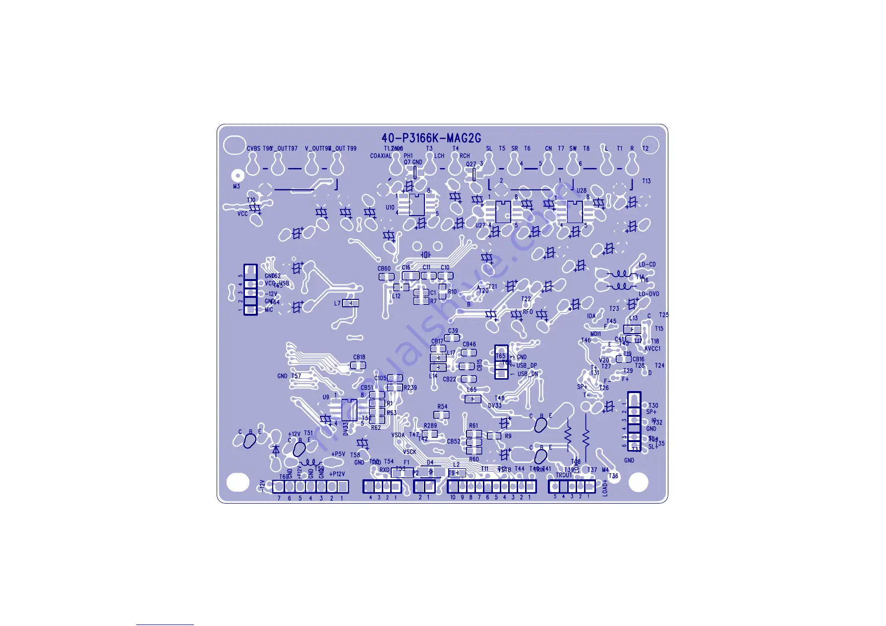
Page 53: ...Great user manuals database on UserManuals info Main Board Print Layout Bottom Side for DVP3156 XX DVP3166 K XX 6 21 6 21 ...
Page 54: ...nuals info 7 1 DVP3156 XX DVP3166 XX Mechanical Exploded View Remark It s a general Mechanical Exploded View for DVP3156 XX DVP3166 XX Detailed information please refer to Model set Ass y1 is the assembled component for location 1 3 4 5 26 ...
Page 55: ...3 Rubber Pad Grounding Pad Ass y USB Board Ass y Front Board for DVP3166 94 Ass y Front Board for DVP3156 93 Ass y US BD 1 Ass y FB BD DVP3166 94 DVP3166x 94 1 Q ty 1 1 1 1 1 1 1 1 1 1 1 1 1 1 1 ENCASING ACCESSORIES PARTS LIST 7 2 SCREW LIST No 1 7 10 12 13 15 18 20 22 12NC No Part Name S T SCREW B 2 6 X 8 BF MACHINE SCREW M C SCREW TRIANGLE W 3 X 6 TRIANGLE M C SCREW B 3 X 6 S T SCREW B 3 X 8 BF ...
Page 56: ...als info 7 3 DVP3160K XX DVP3166K XX Mechanical Exploded View Remark It s a general Mechanical Exploded View for DVP3160K XX DVP3166K XX Detailed information please refer to Model set Ass y1 is the assembled component for location 1 3 4 5 26 ...
Page 57: ... 3 X 6 2 22 S T SCREW B 2 6 X 8 BF 2 14 996510001175 Power Cord for DVP3160K 55 1 996510001227 Power Cord for DVP3160K 77 Power Cord for DVP3160K 78 996510001206 Power Cord for DVP3166K 93 16 996510001198 Rear Cabinet for DVP3160K 55 1 Rear Cabinet for DVP3160K 77 78 Rear Cabinet for DVP3166K 93 18 996510001200 Ass y Power Board for DVP3160K 1 77 78 DVP3166K 93 996510001190 Ass y Power Board for D...
Page 58: ...REVISION LIST Version 1 0 Initial release Version 1 1 Include DVP3166X 94 models Remark This Service manual only for Philips Service repairment Please Don t transmitt or forward it to others 8 1 ...