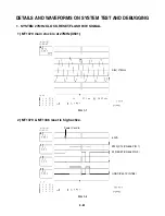
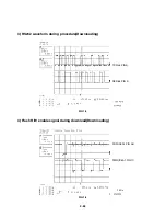
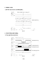
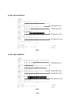

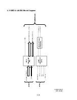


3-75
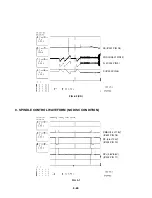
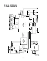
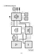
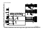
BLOCK DIAGRAMS
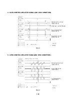
1. Overall Block Diagram
M
M
DISC
SPINDL
E
MO
TO
R
LO
A
D
ING
MO
T
O
R
DECK MECHANISM
DV
D:
RF
0
,A
,B,
C,
D
C
D
:R
F0
,A,B
,C
,D
,E,
F
PICK
UP
KEY In
p
u
t
B/Pb
IC5
A
1
29LV800T
A
-70
1M
8BIT
FL
A
S
H ROM
URST
A[00
:1
9]
PC
E#
PR
D
#
PW
R
#
DQ[00:15]
RFON,R
FOP
,FEO
,R
F
L
,CS
O
T
E
O
,B
D
O
,RFRP,
H
TRC,
V
2
P
8
L/
R
CVBS
R/Pr
G/
Y
Y[1:6]
Y
C
L/
R
VF
+
A
C
90V~240V
50
HZ/60Hz
VF-
-27V
A
5V
3V3M
12V
STBY
,TRCLO
SE
27
M
H
z
X-TA
L
PW
RC
T
L
DV33
IC505
KS24C021C
S
EEPROM
IC401
CS4391(2DA
C
)
IC401
NJ
M
4
580
OP-
A
M
P
RC901
REMOCO
N
RECEIVER
IC903
RESET I
C
LOAD+,LOAD-
F+,F-,T+,T-
SP+,SP-
IC201
MT1336E
RF
SLED
(FEEDING)
MO
T
O
R
SL+,SL-
IC202
L
A
6560
MO
TO
R
DRIVER
M
V3
3
DV33
A
V
33
/DV33
/V25
VCC/DV33/3V3
M
AC
L
K
ABC
L
K
A
L
RCK
IC60
4
MM1
623XFB
E
VIDEO BUFFE
R
M
IC_DETC
ASPDIF
C
O
A
X
O
PT
ICAL
ASPECT
VC
C
RV
CC
AVC
C
AV3
3
V2
5
LD01,LD02
, IOA, V2.
0
VCC/+8V
RVCC
LI
M
IT
TROU
T,
TR
IN
TROPEN
,TRS
O
,F
O
SO
,D
MS
O
,F
M
S
O
°
‹
SC
LK,SDEN,SDAT
A
PW
MOUT
2
AD
[0
:7
]
VC
C
VCR
VFD_SCK
VFD
_
T
X
D
M_RE
Q
POWER
BOARD
V1P4
MD
I1
APC
VFD_R
X
D
S_
R
E
Q
5V2
A
+P8V
MUTE
J6
RS232
TX
D
RX
D
SC
L
IC502
M12L16161
A
512K
2Banks
16BIT
SDR
A
M
SD33
IC503
M12L16161
A
512K
2Banks
16BIT
SDR
A
M
SD33
IC506
M12L64164
A
1M
4Banks
16BIT
SDR
A
M
M
A
[0
0:
10
]
BA0
DCLK
DCK
E
CS
#
RA
S
#
CA
S
#
WE
#
DQM[0:1]
DQ[16:31]
DQM[2:3]
MA11,BA1
SD
A
VRST#
ASDAT[0:3]
VSC
K
VSD
A
ASTB
IC501
MT1379E
DSP/MPEG
+12V
+12
V
VC
C
DV33
IC510
BUFFER IC
74
H
C
T244
VC
C
AD
IN
SD33
COMBI SCART
MTK MODEL
Summary of Contents for DVD755VR
Page 8: ...Directions for Use ...
Page 9: ......
Page 10: ......
Page 11: ......
Page 12: ......
Page 13: ......
Page 14: ......
Page 15: ......
Page 16: ......
Page 17: ......
Page 18: ......
Page 19: ......
Page 20: ......
Page 21: ......
Page 22: ......
Page 23: ......
Page 24: ......
Page 25: ......
Page 26: ...Personal Notes ...
Page 49: ......
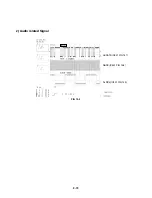
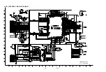
Page 56: ...3 32 3 33 2 TU IF NICAM A2 CIRCUIT DIAGRAM EE MODE VIDEO TU MODE AUDIO COMBI SCART ...
Page 59: ...3 38 3 39 5 SCART JACK CIRCUIT DIAGRAM OPTIONAL PART COMBI SCART ...
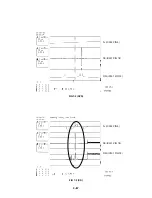
Page 61: ...3 42 3 43 7 TIMER CIRCUIT DIAGRAM ...
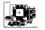
Page 65: ...3 50 3 51 PRINTED CIRCUIT DIAGRAMS 1 MAIN P C BOARD LOCATION GUIDE ...
Page 66: ...3 52 3 53 2 SMPS P C BOARD LOCATION GUIDE 3 TIMER P C BOARD LOCATION GUIDE 4 KEY P C BOARD ...
Page 67: ......
Page 93: ......
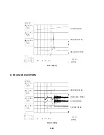
Page 96: ...3 83 3 84 3 AUDIO CIRCUIT DIAGRAM COMBI SCART MTK 03 3 25 SR17447A ...
Page 97: ...3 85 3 86 4 AV JACK CIRCUIT DIAGRAM COMBI SCART MTK 03 3 25 SR17446A ...
Page 100: ...3 91 3 92 PRINTED CIRCUIT DIAGRAMS 1 MAIN P C BOARD LOCATION GUIDE ...
Page 101: ......
Page 133: ...MEMO ...
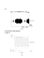
Page 134: ...EXPLODED VIEW 1 Deck Mechanism Exploded View 5 1 CONTENTS SECTION 5 MECHANISM OF DVD PART ...


