background image

Technical Specs, Diversity, and Connections

EN 3

TPS15.3A LA

2.

2015-Oct-23

back to 

div.table 

2.3

Connections

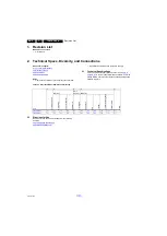
Figure 2-1 Connection overview

Note: The following connector colour abbreviations are used 
(acc. to DIN/IEC 757): Bk= Black, Bu= Blue, Gn= Green, 
Gy= Grey, Rd= Red, Wh= White, Ye= Yellow.

2.3.1

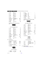
Side Connections

1 - Cinch: SPDIF - Out
Ye - Coaxial 

 0.4 - 0.6V

PP

 / 75 


kq

2 - Audio out
Connect to loudspeaker box or equivalent to output audio.

3 - Mic - in
Bk - Microphone 

80 - 600 

 / 10 mW 

ot

4 - USB1 2.0

Figure 2-2  USB (type A)

1

- +5V 

k

2

- Data (-) 

jk

3

- Data (+) 

jk

4

- Ground Gnd 

H

5 - USB2 2.0

Figure 2-3  USB (type A)

1

- +5V 

k

2

- Data (-) 

jk

3

- Data (+) 

jk

4

- Ground Gnd 

H

6 - TV ANTENNA - In
Signal input from an antenna, cable or satellite.

7 - TV ANTENNA - In
Signal input from an antenna, cable or satellite.

8 - HDMI 2: Digital Video - In, Digital Audio - In/Out

Figure 2-4 HDMI (type A) connector

1

- D2+ Data 

channel 

j

A

u

dio o

u

t

A

u

dio o

u

t

1

2

NET

NETWORK

ORK

PC / DVI 

PC / DVI 

MICMIC

19900_001.eps

1

2

3

4

10

5

6

7

8

9

11

12

13

14

1 2 3 4 

10000_022_090121.eps

090121

1 2 3 4 

10000_022_090121.eps

090121

10000_017_090121.eps

090428

19

1

18

2

Summary of Contents for 6600 series

Page 1: ...nics N V Colour Television Chassis TPS15 3A LA Contents Page Contents Page 1 Revision List 2 2 Technical Specs Diversity and Connections 2 3 Precautions Notes and Abbreviation List 5 4 Mechanical Instructions 9 Cable dressing 49 6600 series 9 Cable dressing 55 6600 series 10 5 Service Modes and Fault Finding 13 6 Alignments 16 7 Circuit Descriptions 17 8 IC Data Sheets 23 9 Block Diagrams Block di...

Page 2: ...ck to div table 2 1 Here is product information available as well as getting started user manuals frequently asked questions and software drivers Table 2 1 Described Model Numbers and Diversity 2 2 Directions for Use Directions for use can be downloaded from the following websites http www philips com support http www p4c philips com CTN 2 4 9 10 11 Connection Overview Mechanics Block Diagrams Sch...

Page 3: ...k Microphone 80 600 10 mW ot 4 USB1 2 0 Figure 2 2 USB type A 1 5V k 2 Data jk 3 Data jk 4 Ground Gnd H 5 USB2 2 0 Figure 2 3 USB type A 1 5V k 2 Data jk 3 Data jk 4 Ground Gnd H 6 TV ANTENNA In Signal input from an antenna cable or satellite 7 TV ANTENNA In Signal input from an antenna cable or satellite 8 HDMI 2 Digital Video In Digital Audio In Out Figure 2 4 HDMI type A connector 1 D2 Data cha...

Page 4: ...S 10 kW jq 11 Audio In PC DVI Left Right Gn Audio L R in 0 5 VRMS 10 k jq 12 PC IN VGA Figure 2 6 VGA connector 1 Video Red 0 7 VPP 75 W j 2 Video Green 0 7 VPP 75 W j 3 Video Blue 0 7 VPP 75 W j 4 n c 5 Ground Gnd H 6 Ground Red Gnd H 7 Ground Green Gnd H 8 Ground Blue Gnd H 9 5VDC 5 V j 10 Ground Sync Gnd H 11 Ground Red Gnd H 12 DDC_SDA DDC data j 13 H sync 0 5 V j 14 V sync 0 5 V j 15 DDC_SCL ...

Page 5: ...the power supply section both in normal operation G and in stand by F These values are indicated by means of the appropriate symbols 3 3 2 Schematic Notes All resistor values are in ohms and the value multiplier is often used to indicate the decimal point location e g 2K2 indicates 2 2 k Resistor values with no multiplier may be indicated with either an E or an R e g 220E or 220R indicates 220 All...

Page 6: ...tion It is easy to do and is a good service precaution 3 4 Abbreviation List 0 6 12 SCART switch control signal on A V board 0 loop through AUX to TV 6 play 16 9 format 12 play 4 3 format AARA Automatic Aspect Ratio Adaptation algorithm that adapts aspect ratio to remove horizontal black bars keeps the original aspect ratio ACI Automatic Channel Installation algorithm that installs TV channels dir...

Page 7: ...sed for broadcast grade video Uncompressed digital component or digital composite signals can be used The SDI signal is self synchronizing uses 8 bit or 10 bit data words and has a maximum data rate of 270 Mbit s with a minimum bandwidth of 135 MHz iTV Institutional TeleVision TV sets for hotels hospitals etc LS Last Status The settings last chosen by the customer and read and stored in RAM or in ...

Page 8: ...SD Standard Definition SDA Serial Data I2C SDA F DAta Signal on Fast I2C bus SDI Serial Digital Interface see ITU 656 SDRAM Synchronous DRAM SECAM SEequence Couleur Avec Mémoire Colour system mainly used in France and East Europe Colour carriers 4 406250 MHz and 4 250000 MHz SIF Sound Intermediate Frequency SMPS Switched Mode Power Supply SoC System on Chip SOG Sync On Green SOPS Self Oscillating ...

Page 9: ...te slightly from the actual situation due to the different set executions 4 1 Cable Dressing Figure 4 1 Cable dressing 49 6600 series 19980_100 eps CN701 CN8101 CN9101 CN403 MAIN POWER SUPPLY 1054 A SSB 1053 B ECN401A ECN601 ECN403 ECN601 LOUDSPEAKER 1184 LOUDSPEAKER 1184 IR LED BOARD 1056 J ECN403 ECN701 E CN01 KEYBOARD CONTROL 1057 CN103 CN601 ECN401A ECN401A ECN701 ECN601 CN401 WIFI MODULE W Wi...

Page 10: ...ow apply to the 49PUH6600 96 but will be similar for 55 model 4 3 1 Rear Cover Refer to Figure 4 3 for details Warning Disconnect the mains power cord before removing the rear cover 1 Remove the fixation screws 1 that secure the base assy pull out the base assy from the set Then remove the fixation screws 2 3 that secure the rear cover Refer to Figure 4 3 for details 2 Gently lift the rear cover f...

Page 11: ...ector 1 that connect with the SSB Caution be careful as these are very fragile connectors Unplug the cable flat foils connector 2 Unplug all other connectors 2 3 Remove all the fixation screws 3 from the SSB 4 Take out the SSB with I O bracket 5 The SSB can now be shifted away from side connector cover then lifted and taken out of the I O bracket Refer to Figure 4 4 for details 6 Unplug the connec...

Page 12: ... DECO_BEZEL When defective replace the whole unit 4 3 8 LCD Panel 1 Remove the SSB as described earlier 2 Remove the PSU as described earlier 3 Remove the keyboard control panel as described earlier 4 Remove the stand as described earlier 5 Remove the IR LED as described earlier 6 Remove the WIFI module as described earlier 7 Remove the fixations screws that fix the metal clamps to the front bezel...

Page 13: ...s the following key sequence on the remote control transmitter from the Menu press 1999 directly followed by the Back button Do not allow the display to time out between entries while keying the sequence After entering the Factory mode the following items are displayed the Default value just for reference Table 5 1 Factory mode overview How to Exit the Factory mode Use one of the following methods...

Page 14: ...e remote control to enter the Factory mode 2 Use the up down cursor keys to select SW Ver If the current software version of the TV is the same as the latest update file found on http www philips com support it is not necessary to update the TV software 5 4 4 Download the latest software 1 Open the internet page http www philips com support 2 Find information and software related to the TV 3 Selec...

Page 15: ... Service are mentioned here EDID_clustername zip Contains the EDID content of the different EDID NVMs See ComPair for further instructions FUS_clustername_version zip Contains the autorun bin which is needed to upgrade the TV main software and the software download application NVM_clustername_version zip Default NVM content Must be programmed via ComPair 5 4 7 How to Copy NVM Data to from USB When...

Page 16: ...i 10 M Ci 20 pF Use an isolated trimmer screwdriver to perform alignments 6 2 Reset of Repaired SSB A very important issue towards a repaired SSB from a Service repair shop SSB repair on component level implies the reset of the NVM on the SSB After a repaired SSB has been mounted in the set set repair on board level the type number CTN and production code of the TV has to be set according to the t...

Page 17: ...see chapter 10 Circuit Diagrams and PWB Layouts Where necessary you will find a separate drawing for clarification 7 1 Introduction The TPS15 3A LA is a new chassis launched in AP in 2015 The whole range is covered by MSD8590QV The major deltas versus its predecessor support PAL NTSC SECAM with multi media Video out function The TPS15 3A LA chassis comes with the following stylings series xxPUH660...

Page 18: ...2015 Oct 23 back to div table 7 1 3 SSB Cell Layout Figure 7 1 SSB layout cells top view 6600 series 19980_200 eps Tuner DC DC USB ANALOG I O PC Audio HDMI HDMI SPDIF Audio out Headphone MSD8590QV XZ ANALOG INPUT USB HDMI NETWORK DC DC DDR DDR ...

Page 19: ... in case of IPB High voltage to the LCD panel PSL and PSLS LED driver outputs PSDL high frequent AC current 7 2 2 Diversity The diversity in power supply units is mainly determined by the diversity in displays The following displays can be distinguished CCFL EEFL backlight power board is conventional IPB LED backlight side view LED without scanning PSL power board side view LED with scanning PSLS ...

Page 20: ...ower 3V3_STB from the power supply for the scaler IC MSD8590QV Figures gives a graphical representation of the DC DC converters with its current consumptions Figure 7 3 DC DC converters 1 6600 series 12V 12V GND 16 15 14 U702 AZ1117D VCC_1V2_CPU Max 6A Max 6A VCC_1V2 U704 G5196R41D DDR_1V5 U707 AT1528P11U Max 2A U705 G5196R41D 4 24V Power Board Input 5VSB P12V P24V 10 3 POWER BOARD 5 GND Q705 AO44...

Page 21: ...ANEL LED Driver 5VSB PANEL VB1 Power P24V Q403 AO4449 7A AMP_24V P12V Main Board Power System For Audio Amplifier Panel For Audio Amplifier U601 AD83586 For Reset IC U701 AP1117E33L 13 77 U406 G690H293T73 3V3_STB VCC_1V2_CPU U705 G5196R41D For MSD8590QV CPU U401 MSD8590QV For MSD8590QV U401 MSD8590QV For Audio ADC U602 WM8782SEDS RV TU101 TDSH T070F TU_3V3 For TUNER 3 3V U708 AZ1117D VCC_3V3 U702 ...

Page 22: ...me Theater Sound Processor Internet and Variety of Connectivity Support Peripheral and Power Management The MSD8590QV combines front end video processing functions such as NTSC PAL SECAM Video Decoder MSD8590QV is a Powerful ARM based Smart TV solution that supports dual 8 10bit LVDS output channel decoding MPEG decoding 3D formatter and media center functionality enabled by a high performance AV ...

Page 23: ...l diagrams with the exception of memory and logic ICs 8 1 Diagram 10 2 9 Karaoke MIC In Audio Output B09 WM8782SEDS RV IC U602 Figure 8 1 Internal block diagram and pin configuration 19980_300 eps Block diagram Pinning information 1 MCLK 2 3 VREFGND 4 5 VREFP 6 7 AVDD 8 AINR 9 AGND 10 AINOPR AINOPL COM AINL M S BCLK FSAMPEN IWL LRCLK DGND DOUT DVDD VMID FORMAT 11 12 13 14 15 16 17 20 19 18 WM8782 ...

Page 24: ...d pin configuration 19980_301 eps Block diagram Pinning information 32 31 30 29 28 27 26 9 10 11 12 13 14 15 16 18 19 20 21 22 23 24 8 7 6 5 4 3 2 1 YSS952 QFN32 Top View 25 17 OPEN DVSS GPIO11 GPIO10 GPIO9 GPIO8 OPEN GPIO0 GPIO1 GPIO7 GPIO6 GPIO5 GPIO4 GPIO3 GPIO2 IOVDD XOUT XIN PLLVDD IC_N SDA SCL IOVDD DVDD18 DVDD18 DVSS PLLVSS IRQ_N TESTb PLLVSS DVSS DVSS YSS952 ...

Page 25: ...3A LA 8 2015 Oct 23 back to div table 8 3 Diagram 10 2 9 Karaoke MIC In Audio Output B09 WM8524CGEDT R IC U604 Figure 8 3 Internal block diagram and pin configuration 19980_302 eps Block diagram Pinning information WM8524 WM8524 ...

Page 26: ...D PGND V V V V OUT TON FB VCC EN BST PGOOD NC 1 AGND LX V 2 3 4 5 6 7 8 9 10 11 12 13 14 15 16 17 18 19 20 21 22 23 24 25 26 27 28 ILIM AGND V5V PGND LX LX LX LX PGND PGND LX LX PGND PGND PGND PGND V V V V OUT TON FB VCC EN BST PGOOD NC G5312QN1U G5312QN1U PWM controller 0 75V Reference PGOOD BST LX PGND TON OUT FB EN ILIM AGND OCP POR On Time Off Time DISCHG VCC OT OVP UVP KV 5V LDO V5V V V5V V D...

Page 27: ...SB 2 0 Port0 VGA AUDIO IN DDR III x 2 4G 1866MHz H5TQ4G63AFR RDC RESET IC G690H293T73 YPbPr Hsync Vsync VIDEO CVBS Share with YPbPr Y VGA RGB YPbPr HDMI 1 DVI HDMI 2 MHL TMDS TMDS TMDS HDMI 3 ARC R L Audio Amplifier AD83586 SPEAKER OUTPUT I2S NOR FLASH ROM MX25L1606EM2I 12G NAND FLASH ROM THGBMBG6D1KBAIL MIC IEC958 SPDIF Output I2S Karaoke DSP YSS952 R L Audio DAC WM8524CGEDT R Audio Lineout Audio...

Page 28: ... 1 3 4 BO C9911 47pF 250V N Vsin C9916 1NF 250V U9901 NC CAP004DG TL NC 1 D1 2 D1 3 NC 4 NC 5 D2 6 D2 7 NC 8 C9907 NC 47PF R9901 NC 510k 1 2W R9902 NC 510k 1 2W GND4 NC GND 1 CN9903 NC CONN L 1 N 2 GND2 NC GND 1 GND1 GND 1 T5AH 250V NC NC C9913 220PF 250V FB9903 BEAD 1 2 C9912 47pF 250V t NR9903 1R 1 2 C9914 220PF 250V t NR9902 1R 1 2 L9902 12mH 1 2 4 3 SG9901 NC DSPL 501N A21F SG9902 NC DSPL 501N...

Page 29: ...1NF 50V R9808 16K 1 1 8W R9807 470K 1 C9807 0 47uF 50V R9809 27K 1 8W 1 C9806 1uF R9810 22K 1 8W 1 C9808 10N 50V C9819 470PF R9811 33K 1 8W 1 C9809 10N 50V R9818 100K 1 8W 1 FB9801 BEAD 1 2 C9818 NC 47PF C9817 100N 50V FB9904 NC BEAD 1 2 C9820 1NF L9801 220uH 6 4 C9816 1NF C9814 47PF For Power Sav ing D9801 FMNS 1106S C9801 68uF 450V C9802 68uF 450V Vbus R9803 1MOHM 1 1 4W R9805 680K OHM 1 1 4W R9...

Page 30: ...101 POWER X FMR 1 2 4 5 6 7 8 10 11 C9307 NC 1uF C9308 NC 1uF C9309 NC 470UF 25V C9122 0 1uF 50V R9105 10ohm 1 1 8W C9112 NC 1uF C9111 NC 1uF R9137 100 OHM 1 4W R9138 510K 1 1 8W PS_ON R9101 0R22 12VS R9305 NC 11K 1 8W 1 DV5 LED_OVP R9306 NC 0R051 8W Q9104 NC 2N7002K R9107 1Kohm 1 1 4W R9307 NC 3K 1 8W 1 R9119 NC 100K 1 8W 1 R9112 27 OHM R9113 27 OHM R9114 27 OHM R9115 27 OHM C9103 330P 50V R9116 ...

Page 31: ...100PF 50V D8102 SS1060FL D8103 SS1060FL R8110 10ohm 1 1 8W R8113 10ohm 1 1 8W ZD8104 BZT52 B30 1 2 R8111 47R 1 R8114 47R 1 R8112 10K 1 8W 1 R8115 10K 1 8W 1 U8103 AS431AN E1 C8124 NC 0 47UF 50V FB_LED FB_LLC FB_LLC R8120 NC 3K 1 8W 5 VS R8166 3K3 1 8W 1 Q8107 LMBT3906LT1G 1 2 3 12V TPV101_VCC R8165 510 OHM 1 1 8W D8110 1N4148W TPV101_VCC U8109 AS431AN E1 R8172 510K 1 1 8W Q8108 2N7002K C8143 0 47U...

Page 32: ...08 J8106 J8121 J9805 J9905 C9105 SU2 SU3 SU4 SU9 SU1 SU8 SU7 SU6 SU5 C9818 C9819 C9820 J8109 J9119 C9106 C9109 C9110 C9309 D9103 F9901 R9901 R9902 U9102 C9301 R9101 T9101 DR1 DR2 DE4 DR7 DR6 DR5 DR8 DR3 C8112 C8108 C8118 C9113 C9115 C8101 C9802 C9801 C9816 C9803 C9804 C9901 C9902 C9913 CN8101 CN9901 CN9903 D9801 FB9901 FB9902 HS8102 HS8103 U8105 U8106 L8101 L9101 L9102 L9301 R9801 R9802 RV9901 SG9...

Page 33: ...115 R9117 R9116 R9302 R9306 R9301 R9307 R9305 R9118 R9119 R9121 R9303 R9304 R9131 R9136 R9138 R9103 R9102 R9108 R9815 R9803 R9814 R9816 R9804 R9808 R9805 R9812 R9813 R9810 R9809 R9811 R9806 R9807 R9908 R9905 R9904 R9907 R9903 R9906 SM9 R9132 R8114 SM12 SM13 U9105 U9801 U9301 R9104 R8111 R9106 JR9101 R8109 R8147 R8148 R8149 R8150 C8139 R8154 R8146 R8145 R8143 R8144 C8138 R8153 C8132 C8131 C8135 C81...

Page 34: ...C0 Tuner IC TDA18273 9 C110 NC 120pF 50V Tuner Reset Active LOW MDI LAN_LED0 7 Differential 100 10 ohms Common Mode 50 5 ohms MDI T and MDI R separate 30mil LAN_LED1 7 088G342GFB1AGN R112 0R05 OHM AIR 11 N_GND 7 1206 10 8 4 VGA Input Back 3D Glasses Launch Place close to U401 Air X15T897320100000BL DDCA_DA 7 R121 75R 1 16W 1 C114 330PF 50V RF Input Side IF Trace C113 330PF 50V 311GB254C20CBX 088G3...

Page 35: ...CN111 RCA JACK 1 2 3 4 6 7 8 9 10 11 12 13 5 1 2 3 4 CN106 USB CONN 1 2 3 4 6 5 ZD122 NC MLVG0402 1 2 C122 NC 10PF 50V R148 10K R146 75R 1 16W 1 C118 10uF 10V ZD116 NC MLVG0402 1 2 C123 330PF 50V AV Input Share with Y Back t TH105 PTCR 1 2 C121 NC 10PF 50V R141 4 7K1 16W ZD118 NC MLVG0402 1 2 ZD112 NC MLVG0402 1 2 R150 12K 1 16W t TH101 PTCR 1 2 KMC3S075RY002 USB trace run 90 Ohm differential pair...

Page 36: ...1 8W C505 NC 10uF 10V HDMI1_D1N HDMI1_CEC HDMI1_D1P D2N 3102 81 HDMI3 ARC Side 3285 91 3246 83 R519 200OHM1 16W D2P HDMITX_CEC 3257 04 D0P CLKP 4775 12 Wake Pulse Sequence 3043 44 C502 47NF 16V D0P D2P MHL CBUS Wake Pulse Sequence D0N 3159 26 3141 48 HDMI 1 Trace mil D2N 3116 3 U505 AZ1045 04F R7G IN1 1 IN2 2 GND 3 IN3 4 IN4 5 NC 6 NC 7 GND 8 NC 9 NC 10 space trace space gnd space trace space mil ...

Page 37: ...0QV XZ U401D RX0N R3 RX0P R2 RX1N R1 RX1P T3 RX2N T1 RX2P T2 RXCN P3 RXCP P2 DDCDA_CK U5 DDCDA_DA V5 HOTPLUGA U6 ARC0 M4 D_RX0N M3 D_RX0P M2 D_RX1N M1 D_RX1P N3 D_RX2N N1 D_RX2P N2 D_RXCN L3 D_RXCP L2 DDCDD_CK N5 DDCDD_DA M5 HOTPLUGD L5 C_RX0N AH7 C_RX0P AF8 C_RX1N AH8 C_RX1P AG8 C_RX2N AF9 C_RX2P AG9 C_RXCN AF7 C_RXCP AG7 DDCDC_CK AD6 DDCDC_DA AC6 HOTPLUGC AD7 AVDD5V_HDMI_C AE5 CEC U4 DM_P0 D1 DP...

Page 38: ...EMMC_CMD AH17 EMMC_RSTN AF17 NAND_ALE AG15 NAND_CEZ AG16 NAND_CEZ1 AF16 NAND_CLE AH14 NAND_RBZ AF15 NAND_REZ AG14 NAND_WEZ AF14 NAND_WPZ AH16 PCM_A 0 AG20 PCM_A 1 AH20 PCM_A 2 AF20 PCM_A 3 AH19 PCM_A 4 AG19 PCM_A 5 AF19 PCM_A 6 AG18 PCM_A 7 AF18 PCM_A 8 AE10 PCM_A 9 AC11 PCM_A 10 AD11 PCM_A 11 AE11 PCM_A 12 AC12 PCM_A 13 AD12 PCM_A 14 AE13 PCM_D 0 AE7 PCM_D 1 AD9 PCM_D 2 AC8 PCM_D 3 AE8 PCM_D 4 AD...

Page 39: ...1V5 R485 22 OHM 1 16W R487 22 OHM 1 16W C437 10N 50V RP427 22R 1 2 3 4 8 7 6 5 RP435 22R 1 2 3 4 8 7 6 5 RP439 22R 1 2 3 4 8 7 6 5 RP433 22R 1 2 3 4 8 7 6 5 RP429 22R 1 2 3 4 8 7 6 5 RP423 22R 1 2 3 4 8 7 6 5 RP431 22R 1 2 3 4 8 7 6 5 RP425 22R 1 2 3 4 8 7 6 5 RP437 22R 1 2 3 4 8 7 6 5 Shield by GND alone C465 100N16V B DDR3 DQL1 B DDR3 ODT B DDR3 DQU4 B DDR3 DQU0 B DDR3 DQU2 B DDR3 DQU5 B DDR3 DQ...

Page 40: ...D33_LAN P9 U_AVDDL_MOD T25 U_AVDDL_PREDEV U25 C471 100N16V VCC_1V2 VCC_1V2 C470 1UF 6 3V FB407 300R 1 2 VCC_3V3 C499 100N16V C497 100N16V TP4 1 C481 100N16V DDR_1V5 C482 1UF 6 3V 3V3_STB C483 100N16V MSD8590QV XZ U401G GND J21 GND J22 GND J23 GND J28 GND K7 GND K8 GND K12 GND H19 GND K21 GND K28 GND L7 GND L8 GND L12 GND L13 GND L14 GND L15 GND L16 GND L17 GND L21 GND M7 GND M8 GND M9 GND M11 GND ...

Page 41: ...or POP Noise 22uH Speaker Output 388G078G111ACL Lo 10uH 073G253S 81 Y 22uH 373G253S193D00 47uH 373G253S173Y00 47uH 0805 C604 C607 C613 C619 C622 C629 AMP_24V Hi AMP_24V 0x6A SubWoofer Output CFG0 24V R R Hi L601 L602 L603 L604 L605 L606 L 0603 Coaxial 16 ohm 680nF 50V Lo SA1 0603 0603 L FB603 NC 600 OHM 1 2 1206 P90T0066101 5VSB R627 10K C633 100UF 16V R628 100K1 16W D601 LL4148 FB602 600 OHM 1 2 ...

Page 42: ...DO0 10 C650 100N16V C648 100N16V C649 100N16V VMID C638 10uF 10V R642 2K OHM R646 3 3K 1 16W R649 2K OHM C641 10uF 10V R644 82K 1 C653 100N16V R674 0R05 OHM C654 100N16V VCC_3V3 R678 10K DSP_IRQ U602 WM8782SEDS RV MCLK 1 DOUT 2 LRCLK 3 DGND 4 DVDD 5 BCLK 6 IWL 7 FSAMPEN 8 FORMAT 9 VMID 10 VREFGND 11 VREFP 12 AVDD 13 AGND 14 AINOPR 15 AINR 16 COM 17 AINOPL 18 AINL 19 M S 20 Audio Interface Mode 0 2...

Page 43: ... 7 C3M 7 C4M 7 C1M 7 B4P B0P 7 C4P 7 3D_LR_O CCKP C0M B4M 7 C4P R4G8 NC 33 OHM 1 16W C2P C2M 3D_L_R_O B2P 7 B2P B1P CCKM 7 C4M C3P C1M C3P 7 BCKM LR_SYNC 7 LR_SYNC LVDS_SEL R4D1 NC 33 OHM 1 16W HTPDN LOCKN C4E2 NC 0 1uF 50V M_SDA 7 10 11 13 R4D2 NC 33 OHM 1 16W M_SCL M_SCL 7 10 11 13 SCL R4D3 NC 33 OHM 1 16W 3D_L_R_O 3 RP441 NC 0OHM 1 16W 1 2 3 4 8 7 6 5 PANEL_POWER R4C5 10K R4C3 150K B3P Q404 MMB...

Page 44: ...M R224 NC 33 OHM 1 16W M_SDA C213 NC 1nF 50V C216 NC 1nF 50V R245 NC 100OHM R232 NC 33 OHM 1 16W R227 NC LED_B6 R243 NC R226 NC 4 7K1 16W R225 NC 4 7K1 16W LED_B0 LED_B1 R239 NC 4 7K1 16W R237 NC R242 NC 4 7K1 16W R229 NC LED_B3 LED_B4 R231 NC 4 7K1 16W VCC_3V3 R240 NC 4 7K1 16W R228 NC R241 NC 4 7K1 16W R238 NC R230 NC LED_B5 LED_B2 LED_R_G LED_R_R LED_R_B LED_VCC LED_VCC LED_L_R LED_L_B LED_L_G ...

Page 45: ...5 7 15K 1 R735 10K VID0 7 TU_3V3 3 C728 100N16V R738 100K1 16W VID1 7 C731 10uF 10V C736 10N 50V C754 10uF 10V R763 NC 4 7K1 16W R758 NC 6K8 C729 10uF 10V VCC_5V R746 499 1 1 10W VCC_5V 3 4 7 11 13 3V3_STB R748 180K C759 1UF16V R722 20K 1 16W VCC_1V2_CPU 9 3V3_STB 5VSB 3 5 10 11 C739 470PF 50V R725 10K R750 20K 1 16W C744 NC R775 NC 47K 0603 0603 C Q711 NC AO4449 7A 30V S 1 S 2 S 3 G 4 D 8 D 7 D 6...

Page 46: ...6 ZD507 ZD508 ZD509 ZD510 ZD511 ZD601 ZD602 ZD603 ZD604 ZD605 U407 L 1 0 1 CN103 U704 U603 R101 R102 R106 R 1 0 5 R107 R108 R110 R 1 0 9 R111 R112 R 1 1 3 R114 R 1 1 5 R118 R119 R122 R121 R124 R123 R126 R127 R128 R129 R130 R131 R132 R133 R134 R135 R136 R138 R141 R142 R143 R144 R145 R146 R148 R149 R150 R151 R154 R155 R158 R159 R4D3 R4D2 R244 R246 R226 R238 R251 R443 R444 R450 R451 R453 R458 R462 R4...

Page 47: ...RP436 RP419 RP438 RP421 RP435 SEN3 Q401 D601 C441 C444 C445 C420 C446 C465 C449 C466 C467 C468 C448 C427 C460 C497 C499 C4A1 C4A2 C4A3 C4A4 C4A5 C4A8 C4A9 C443 C4B3 C4B4 C4B5 C488 C496 C634 C642 C653 C739 C744 R116 R117 R430 R429 R433 R436 R437 R438 R447 R449 R448 R452 R456 R464 R467 R491 R439 R470 R421 R427 R432 R501 R502 R509 R510 R511 R513 R515 R520 R524 R526 R535 R538 R539 R540 R541 R542 R605 ...

Page 48: ...BC847C LED210 LED 2 1 LED209 GPTS06033RC3 PB 1 2 R235 49 9 OHM 1 1 16W ZD204 MLVG0402 1 2 C208 1uF 10V RC6 R223 100OHM C207 NC 100P 50V R222 2K7 1 16W 5 3V3SB IR U202 TSOP75436WTT GND 1 Vs 2 OUT 3 GND 4 ZD204 close to U202 R244 0R05 1 16W U203 ALS PDIC17 55C TR8 OUT 1 VCC 2 GND 3 GND 4 R238 NC 2M OHM 1 16W 5 C209 1uF 10V R227 22K1 16W R229 100K1 16W C214 100P 50V U205 LM358APWR 1OUT 1 1IN 2 1IN 3 ...

Page 49: ...nel layout top bottom 2015 06 02 R250 C211 R249 C210 C207 C208 LED208 LED209 LED210 Q201 Q202 R220 R221 R222 R223 R224 R238 U202 U203 ZD202 ZD203 ZD204 ZD2 ZD3 ZD201 C209 C212 C213 C214 R225 R227 R228 R229 R230 R231 R232 R233 R234 R235 R236 R239 R240 R244 U205 ZD1 ZD4 CN201 R252 R251 Layout IR LED panel top side Layout IR LED panel bottom side ...

Page 50: ...ICSDAT Gaming 3D_L R Wireless_L R Q202 AO3414 Lighting LOGO R230 1K 1 16W 5 R232 2R2 1 16W 5 DVD3V3 3V3SB LED205 CHIP LED WHITE 99 113UNC 2223010 TR8 2 1 LED206 CHIP LED WHITE 99 113UNC 2223010 TR8 2 1 R231 2R2 1 16W 5 3V3SB LOGO R205 NC 0R05 1 16W U203 NC JSA 1130 ADDR 1 VDD 2 GND 3 SCL 4 SDA 5 INT 6 R213 NC 0R05 1 16W Light Sensor R209 NC 10K 1 16W 5 Digital Light Sensor C202 NC 1uF 10V R208 NC ...

Page 51: ...7074 IR LED panel layout top bottom LED206 LED201 LED205 U203 LED202 LED203 LED204 R217 R216 R218 R219 R229 Q202 R231 R206 R205 R203 R204 R233 R202 C205 C204 R215 Q207 Q201 R234 R211 R212 U202 C203 R210 R209 R208 CN201 R232 C202 C201 R201 R213 R214 U201 ZD201 R230 R207 Layout IR LED panel top side Layout IR LED panel bottom side ...

Page 52: ...ht Left Down Up R04 2K2 1 10W 1 R01 1K2 1 10W 1 6 5 short 2 5 short F1 3 5 short 1 5 short 4 5 short F2 F3 F4 F5 Direction switch C06 100N 50V Joystick circuit diagram pin1 0V 0 5V 0 81V 1 65V 2 27V pin2 No function pin3 3 3V C04 NC 100N 50V pin4 C05 NC 100N 50V pin5 pin6 C01 NC 100N 50V C02 NC 100N 50V C03 NC 100N 50V p U r e t n e C Down R02 0R05 1 10W 0R 2K2 Resistance Key function Center CH CH...

Page 53: ...div table 10 5 2 Key board layout 19610_546 eps 2013 09 17 1 715G6316 Keyboard control panel layout top bottom SW2 SW3 SW4 SW5 SW6 SW7 CN01 C01 C02 C03 C04 C05 C06 R01 R02 R03 R04 R05 R1 R2 SW01 Layout Keyboard control panel top side Layout Keyboard control panel bottom side ...

Page 54: ... 1 10W 1 1 5 short 4 5 short F2 F3 F5 F3 F1 F4 F2 SW01 TACT SW 6P 3 4 2 1 6 5 7 8 F4 F5 R05 15K 1 10W 1 Direction R03 6K8 1 10W 1 switch Joystick circuit diagram C06 0 1uF 50V pin1 0V 0 5V 0 81V 1 65V 2 27V pin2 No function pin3 3 3V C04 NC 100N 50V pin4 pin5 C05 NC 100N 50V pin6 C01 NC 100N 50V C02 NC 100N 50V C03 NC 100N 50V Down Up Center CN01 CONN 1 2 3 4 R02 0R05 1 10W 0R 2K2 Key functionResi...

Page 55: ...iv table 10 6 2 Key board layout 19850_525 eps 2014 06 06 715G7088 Keyboard control panel layout top bottom C01 C02 C03 C04 C05 C06 R01 R02 R03 R04 R05 H1 H2 H3 H4 H5 H6 CN01 SW01 SW1 SW2 SW3 SW4 Layout Keyboard control panel top side Layout Keyboard control panel bottom side ...

Page 56: ...20DBX CABLE 3 Power Consumption 6 11 HIGH AIR LOW 1 4 RF Switch Control 8 10 5 Tuner Reset Active LOW 2 7 9 Cable I2C Address 0xC0 Tuner IC TDA18273 Air TU101 TDSH T070F RF S W CTL 1 Reset 2 B1 5 NC 8 TH1 12 TH2 13 TH3 14 TH4 15 SCL 3 SDA 4 NC 6 NC 7 IF_AGC 9 DIF1 P 10 DIF2 N 11 3V3T RF_CTRL TU_RESET TU_SCL TU_SDA IF_AGC DIF1 DIF2 CN1001 CONN 1 3 5 7 9 11 13 15 17 19 2 4 6 8 10 12 14 16 18 20 ...

Page 57: ...57 TPS15 3A LA 10 2015 Oct 23 back to div table 10 7 2 TunerBox Board layout 19740_515 eps 715G6344 TunerBox Board layout top bottom TU101 TU13 TU14 CN1001 TU2 TU12 TU1 TU11 Layout TunerBox Board top side Layout TunerBox Board bottom side ...

Page 58: ...S SEE WIRING DIAGRAM CHAPTER 9 Pos No Description Remarks 0030 Bezel 0040 Rear cover 0050 Stand Assy 0095 V0 Sheet 1050 Display panel 1053 Panel SSB 1054 Power Supply Unit 1056 IR LED panel 1057 Keyboard control panel 1067 Tuner board 1176 Remote control Not displayed 1184 Speakers WiFi01 WiFi_USB 0050 0095 0040 1054 1057 1050 1056 1184 1184 1053 0030 1067 WiFi01 ...

Page 59: ...ING DIAGRAM CHAPTER 9 Pos No Description Remarks 0030 Bezel 0040 Rear cover 0050 Stand Assy 0095 V0 Sheet 1050 Display panel 1053 Panel SSB 1054 Power Supply Unit 1056 IR LED panel 1057 Keyboard control panel 1067 Tuner board 1176 Remote control Not displayed 1184 Speakers WiFi01 WiFi_USB 0050 0095 0040 1054 1057 1050 1056 1184 1184 1053 0030 1067 WiFi01 ...

Reviews: