background image

Service Modes and Fault Finding

EN 32

TPN10.1E LA

5.

2013-Oct-18

back to 

div. table

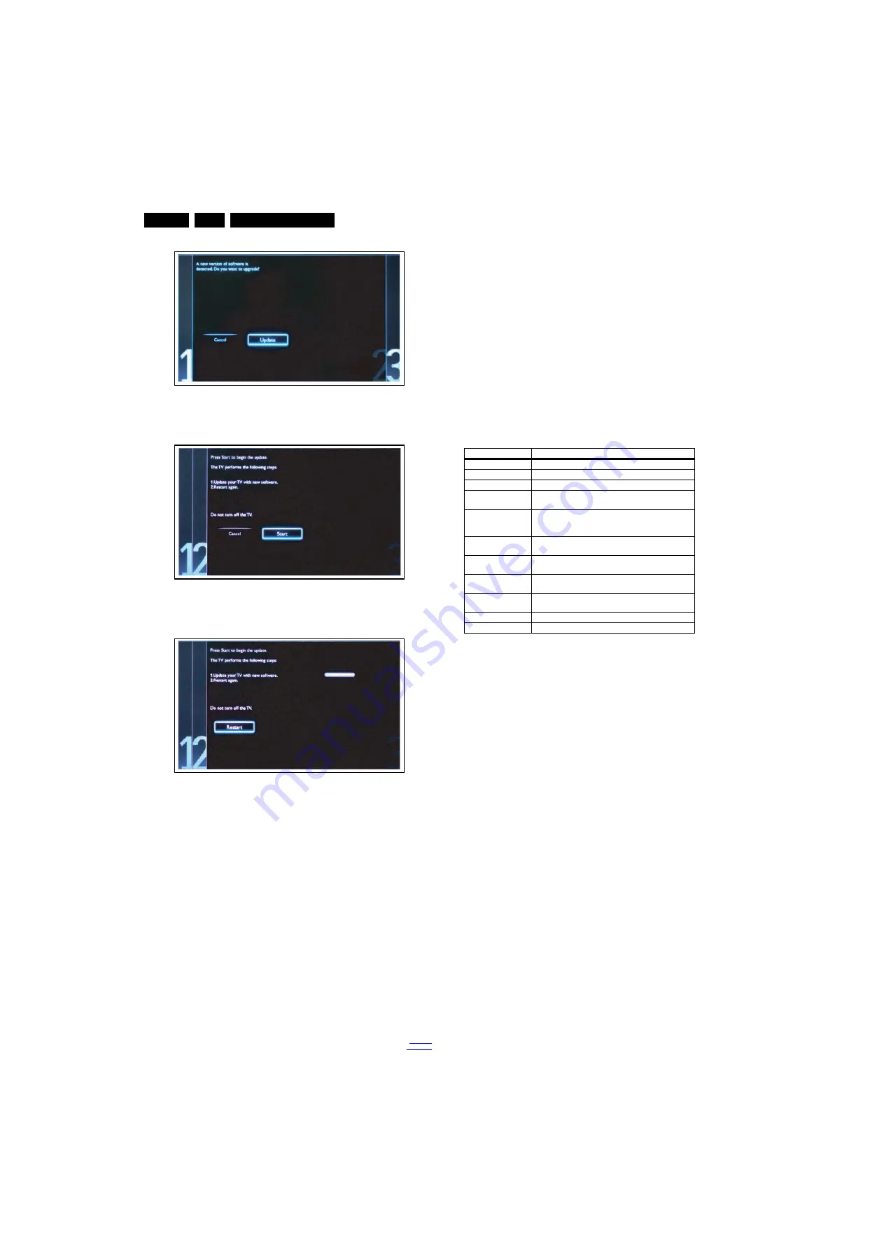
Figure 5-3 Update the TV software [1/3]

Figure 5-4 Update the TV software [2/3]

Figure 5-5 Update the TV software [3/3]

Note:

Do not remove the USB flash drive during the software 
update.

If a power failure occurs during the update, do not remove 
the USB flash drive from the TV. The TV will continue the 
software update as soon as the power comes up again.

If an error occurs during the update retry the procedure or 
contact the dealer.

We do not recommend downgrading to an older version.

Once the upgrade is finished, use the PC to remove the TV 
software from the USB portable memory.

5.5.6

Content and Usage of the One-Zip Software File

Below you find a content explanation of the One-Zip file, and 
instructions on how and when to use it. Only files that are 
relevant for Service are mentioned here. 

EDID_clustername.zip: Contains the EDID content of the 
different EDID NVMs. See ComPair for further instructions.

FUS_clustername_version.zip: Contains the file 
downloaded which is needed to upgrade the TV main 
software and the software download application.

NVM_clustername_version.zip: Default NVM content. 
Must be programmed via ComPair.

5.5.7

How to Copy NVM Data to/from USB

When copying data to and from a USB memory stick, the folder 
“repair” is used. When inserting an empty USB memory stick, 
and downloading data to the stick, the TV will create this folder. 
When sending data from a USB memory stick to a TV, the 
intended data must be available in the “repair” folder.
Note that when copying EDID data to the TV, all necessary 
EDID files must be in this folder.
Service mode overview for your reference.

Table 5-3 Service mode overview

5.6

The Blinking LED Procedure

5.6.1

Introduction

The software is capable of identifying different kinds of errors. 
Because it is possible that more than one error can occur over 
time, an error buffer is available, which is capable of storing the 
last five errors that occurred. This is useful if the OSD is not 
working properly.
Errors can also be displayed by the blinking LED procedure. 
The method is to repeatedly let the front LED pulse with as 
many pulses as the error code number, followed by a period of 
1.5 seconds in which the LED is “off”. Then this sequence is 
repeated. 
Example (1): error code 4 will result in four times the sequence 
LED “on” for 0.25 seconds / LED “off” for 0.25 seconds. After 
this sequence, the LED will be “off” for 1.5 seconds. Any RC 
command terminates the sequence. Error code LED blinking is 
in red color.
Example (2): the content of the error buffer is “12 9 6 0 0” After 
entering SDM, the following occurs.

1 long blink of 5 seconds to start the sequence.

12 short blinks followed by a pause of 1.5 seconds.

9 short blinks followed by a pause of 1.5 seconds.

6 short blinks followed by a pause of 1.5 seconds.

1 long blink of 1.5 seconds to finish the sequence.

The sequence starts again with 12 short blinks.

5.6.2

Displaying the Entire Error Buffer 

Additionally, the entire error buffer is displayed when Service 
Mode “SDM” is entered.

19080_207_110324.eps 

110324 

19080_208_110324.eps 

110324 

19080_209_110324.eps 

110324 

Service Modes

Description

SAM

Service alignment mode

Factory Mode

Used for extended alignments

SDM

Service default Mode

CSM

3-page compact CSM pages. There will be CSM dump to 
USB-stick upon entering CSM-mode

USB SW upgradeable SW-upgrading of flash memories can be done via USB. 

The main SW can be upgraded via the ZIP file 
downloaded.

NVM-Editor in SAM

NVM-editor will function as in the past: Address and Value 
field is a decimal value via digit entry

Service Data

New Service data in SAM for CTN, Prod. no., 12NC 
programming with virtual keyboard

USB copy/paste in 
SAM

Channel list, NVM data, Readable info, EDID

UART logging

There will be printout available in UART. No specifications 
of the printout, per platform provision/definition.

Blind SAM

RC sequence “062598” + “Menu” + “Panel code”

Clear Buffer

RC sequence “062599” + “OK” or via SAM

Summary of Contents for 39PFL4398T/60

Page 1: ...Notes and Abbreviation List 11 4 Mechanical Instructions 15 5 Service Modes and Fault Finding 26 6 Alignments 34 7 Circuit Descriptions 36 8 IC Data Sheets 47 9 Block Diagrams Wiring diagram 3000 series 24 59 Wiring diagram 3000 series 32 60 Wiring diagram 3000 series 39 61 Wiring diagram 31x8H 12 series 40 62 Wiring diagram 31x8T 60 series 40 63 Wiring diagram 31x8H 12 series 42 47 64 Wiring diag...

Page 2: ...trol board IR LED panel 20PFL3108H 12 2 18 4 1 4 15 4 16 9 1 9 8 10 2 10 4 10 6 11 1 22PFL3108H 60 2 18 4 1 4 15 4 16 9 1 9 8 10 2 10 4 10 6 11 2 24PFL3108H 12 2 18 4 1 4 15 4 16 9 1 9 8 10 2 10 4 10 6 11 3 24PFL3108H 60 2 18 4 1 4 15 4 16 9 1 9 8 10 2 10 4 10 6 11 3 32PFL3088H 12 2 1 4 2 4 8 4 10 4 11 9 2 9 8 10 3 10 7 11 4 32PFL3148H 12 2 1 4 2 4 8 4 10 4 11 9 2 9 8 10 3 10 7 11 4 32PFL3168H 12 ...

Page 3: ...ARC In Out Figure 2 3 HDMI type A connector 1 D2 Data channel j 2 Shield Gnd H 3 D2 Data channel j 4 D1 Data channel j 5 Shield Gnd H 6 D1 Data channel j 7 D0 Data channel j 8 Shield Gnd H 9 D0 Data channel j 10 CLK Data channel j 11 Shield Gnd H 12 CLK Data channel j 13 Easylink CEC Control channel jk 14 ARC Audio Return Channel k 15 DDC_SCL DDC clock j 16 DDC_SDA DDC data jk 17 Ground Gnd H 18 5...

Page 4: ... H 4 Service UART 1 Ground Gnd H 2 UART_TX Transmit k 3 UART_RX Receive j 8 EXT1 Video RGB YC In CVBS In Out Audio In Out Figure 2 5 SCART connector 1 Audio R 0 5 VRMS 1 k k 2 Audio R 0 5 VRMS 10 k j 3 Audio L 0 5 VRMS 1 k k 4 Ground Audio Gnd H 5 Ground Blue Gnd H 6 Audio L 0 5 VRMS 10 k j 7 Video Blue C out 0 7 VPP 75 jk 8 Function Select 0 2 V INT 4 5 7 V EXT 16 9 9 5 12 V EXT 4 3 j 9 Ground Gr...

Page 5: ... 3 D2 Data channel j 4 D1 Data channel j 5 Shield Gnd H 6 D1 Data channel j 7 D0 Data channel j 8 Shield Gnd H 9 D0 Data channel j 10 CLK Data channel j 11 Shield Gnd H 12 CLK Data channel j 13 Easylink CEC Control channel jk 14 n c 15 DDC_SCL DDC clock j 16 DDC_SDA DDC data jk 17 Ground Gnd H 18 5V j 19 HPD Hot Plug Detect j 20 Ground Gnd H 5 HDMI 1 Digital Video In Digital Audio with ARC In Out ...

Page 6: ...one 80 600 10 mW ot 9 EXT1 Video RGB YC In CVBS In Out Audio In Out Figure 2 10 SCART connector 1 Audio R 0 5 VRMS 1 k k 2 Audio R 0 5 VRMS 10 k j 3 Audio L 0 5 VRMS 1 k k 4 Ground Audio Gnd H 5 Ground Blue Gnd H 6 Audio L 0 5 VRMS 10 k j 7 Video Blue C out 0 7 VPP 75 jk 8 Function Select 0 2 V INT 4 5 7 V EXT 16 9 9 5 12 V EXT 4 3 j 9 Ground Green Gnd H 10 n c 11 Video Green 0 7 VPP 75 j 12 n c 1...

Page 7: ...ital Audio In Out Figure 2 13 HDMI type A connector 1 D2 Data channel j 2 Shield Gnd H 3 D2 Data channel j 4 D1 Data channel j 5 Shield Gnd H 6 D1 Data channel j 7 D0 Data channel j 8 Shield Gnd H 9 D0 Data channel j 10 CLK Data channel j 11 Shield Gnd H 12 CLK Data channel j 13 Easylink CEC Control channel jk 14 n c 15 DDC_SCL DDC clock j 16 DDC_SDA DDC data jk 17 Ground Gnd H 18 5V j 19 HPD Hot ...

Page 8: ... Data channel j 13 Easylink CEC Control channel jk 14 n c 15 DDC_SCL DDC clock j 16 DDC_SDA DDC data jk 17 Ground Gnd H 18 5V j 19 HPD Hot Plug Detect j 20 Ground Gnd H 9 Cinch Digital Audio Out BK Coaxial 0 4 0 6VPP 75 W kq 10 Head phone Output Bk Head phone 80 600 10 mW ot 11 Service UART 1 Ground Gnd H 2 UART_TX Transmit k 3 UART_RX Receive j 12 EXT1 Video RGB YC In CVBS In Out Audio In Out Fig...

Page 9: ...C IN VGA Figure 2 20 VGA connector 1 Video Red 0 7 VPP 75 W j 2 Video Green 0 7 VPP 75 W j 3 Video Blue 0 7 VPP 75 W j 4 n c 5 Ground Gnd H 6 Ground Red Gnd H 7 Ground Green Gnd H 8 Ground Blue Gnd H 9 5VDC 5 V j 10 Ground Sync Gnd H 11 Ground Red Gnd H 12 DDC_SDA DDC data j 13 H sync 0 5 V j 14 V sync 0 5 V j 15 DDC_SCL DDC clock j 6 HDMI 1 Digital Video In Digital Audio with ARC In Out Figure 2 ...

Page 10: ... phone 80 600 10 mW ot 10 EXT1 Video RGB YC In CVBS In Out Audio In Out Figure 2 22 SCART connector 1 Audio R 0 5 VRMS 1 k k 2 Audio R 0 5 VRMS 10 k j 3 Audio L 0 5 VRMS 1 k k 4 Ground Audio Gnd H 5 Ground Blue Gnd H 6 Audio L 0 5 VRMS 10 k j 7 Video Blue C out 0 7 VPP 75 jk 8 Function Select 0 2 V INT 4 5 7 V EXT 16 9 9 5 12 V EXT 4 3 j 9 Ground Green Gnd H 10 n c 11 Video Green 0 7 VPP 75 j 12 n...

Page 11: ...the power supply section both in normal operation G and in stand by F These values are indicated by means of the appropriate symbols 3 3 2 Schematic Notes All resistor values are in ohms and the value multiplier is often used to indicate the decimal point location e g 2K2 indicates 2 2 k Resistor values with no multiplier may be indicated with either an E or an R e g 220E or 220R indicates 220 All...

Page 12: ...ation It is easy to do and is a good service precaution 3 4 Abbreviation List 0 6 12 SCART switch control signal on A V board 0 loop through AUX to TV 6 play 16 9 format 12 play 4 3 format AARA Automatic Aspect Ratio Adaptation algorithm that adapts aspect ratio to remove horizontal black bars keeps the original aspect ratio ACI Automatic Channel Installation algorithm that installs TV channels di...

Page 13: ...used for broadcast grade video Uncompressed digital component or digital composite signals can be used The SDI signal is self synchronizing uses 8 bit or 10 bit data words and has a maximum data rate of 270 Mbit s with a minimum bandwidth of 135 MHz iTV Institutional TeleVision TV sets for hotels hospitals etc LS Last Status The settings last chosen by the customer and read and stored in RAM or in...

Page 14: ...SD Standard Definition SDA Serial Data I2C SDA F DAta Signal on Fast I2C bus SDI Serial Digital Interface see ITU 656 SDRAM Synchronous DRAM SECAM SEequence Couleur Avec Mémoire Colour system mainly used in France and East Europe Colour carriers 4 406250 MHz and 4 250000 MHz SIF Sound Intermediate Frequency SMPS Switched Mode Power Supply SoC System on Chip SOG Sync On Green SOPS Self Oscillating ...

Page 15: ... Service Positions 4 3 Assembly Panel Removal for 32 39 4 4 Assembly Panel Removal for 40 42 47 4 5 Assembly Panel Removal for 20 22 24 4 6 Set Re assembly Notes Figures below can deviate slightly from the actual situation due to the different set executions 4 1 Cable Dressing Figure 4 1 Cable dressing 24 3000 series 19531_100_130827 eps 130827 ...

Page 16: ...nical Instructions EN 16 TPN10 1E LA 4 2013 Oct 18 back to div table Figure 4 2 Cable dressing 32 3000 series Figure 4 3 Cable dressing 39 3000 series 19530_100_130725 eps 130725 19530_101_130729 eps 130729 ...

Page 17: ...l Instructions EN 17 TPN10 1E LA 4 2013 Oct 18 back to div table Figure 4 4 Cable dressing 40 31x8H 12 series Figure 4 5 Cable dressing 40 31x8T 60 series 19530_102_130729 eps 130729 19530_103_130729 eps 130729 ...

Page 18: ...l Instructions EN 18 TPN10 1E LA 4 2013 Oct 18 back to div table Figure 4 6 Cable dressing 47 31x8H 12 series Figure 4 7 Cable dressing 47 31x8T 60 series 19530_104_130729 eps 130729 19530_105_130729 eps 130729 ...

Page 19: ...ESD safe measures are taken 4 3 Assembly Panel Removal for 32 39 Instructions below apply to the 32PFL3168T 60 but will be similar for other series models 4 3 1 Rear Cover Refer to Figure 4 8 for details Warning Disconnect the mains power cord before removing the rear cover 1 Remove fixation screws 1 that secure the base assy pull out the base assy from the set Then remove the fixation screws 2 3 ...

Page 20: ...ift the speakers cover from the TV Make sure that wires and cables are not damaged while lifting the rear cover from the set 3 Remove the fixation screws 1 that secure the speakers Refer to Figure 4 10 for details 4 Gently take the cable 2 out from the snap Then gently unplug the connectors 3 from the SSB PSU combination panel Refer to Figure 4 10 for details 5 Gently take the speakers out When de...

Page 21: ...bination panel 1 Caution be careful as these are very fragile connectors 2 Unplug all other connectors 2 3 3 Remove all the fixation screws from the SSB PSU combination panel 4 4 The SSB PSU combination panel can now be shifted from side connector cover then lifted and taken out of the I O bracket Refer to Figure 4 11 for details Figure 4 11 SSB PSU combination panel removal 4 3 4 Stand bracket 1 ...

Page 22: ...ot release from bezel When defective replace the whole unit 4 4 Assembly Panel Removal for 40 42 47 Instructions below apply to the 40PFL3188T 60 but will be similar for other series models 4 4 1 Rear Cover Refer to Figure 4 12 for details Warning Disconnect the mains power cord before removing the rear cover 1 Remove fixation screws 1 that secure the base assy pull out the base assy from the set ...

Page 23: ...igure 4 14 for details Caution it is mandatory to remount all different screws at their original position during re assembly Failure to do so may result in damaging the SSB 1 Release the clips from the LVDS connector that connect with the SSB 1 Caution be careful as these are very fragile connectors 2 Unplug all other connectors 2 3 Remove all the fixation screws from the SSB 3 4 The SSB can now b...

Page 24: ...e 4 15 for details Warning Disconnect the mains power cord before removing the rear cover 1 Remove fixation screws 1 that secure the base assy pull out the base assy from the set Then remove the fixation screws 2 that secure the rear cover Refer to Figure 4 15 for details 2 At the indicated areas 3 the cover is secured by clips Be very careful with releasing those 3 Gently lift the rear cover from...

Page 25: ...panel 1 Remove the stand bracket as described earlier 2 Unplug the connector from the IR LED panel 3 Gently release the clip that holds the panel and take it out from the bezel When defective replace the whole unit 4 5 7 LCD Panel 1 Unplug all the connector cables of the boards 2 Gently take all the speakers out 3 Lift the subframe with SSB PSU IR LED panel from the LCD panel and put it aside Warn...

Page 26: ...e general Life Timer During the life time cycle of the TV set a timer is kept called Op Hour It counts the normal operation hours not the Stand by hours The actual value of the timer is displayed in SDM and SAM in a decimal value Every two soft resets increase the hour by 1 Stand by hours are not counted Software Identification Version and Cluster The software ID version and cluster will be shown ...

Page 27: ...ion settings display Error buffer clearing Option settings Software alignments White Tone NVM Editor Set screen mode to full screen all content is visible How to Activate SAM To activate SAM use one of the following methods Press the following key sequence on the remote control transmitter 062596 directly followed by the INFO OK button Do not allow the display to time out between entries while key...

Page 28: ...eful changing this it can result in not correct displaying the screen 3 DB COPY TV to USB Press OK DB COPY TV to USB 4 DB READ USB to TV Press OK DB READ USB to TV 5 CLR_TEMP_R 68 68 68 128 128 118 128 128 Red colour temperature setting 6 CLR_TEMP_G 76 76 76 128 128 128 128 128 Green colour temperature setting 7 CLR_TEMP_B 128 128 128 128 128 126 128 128 Blue colour temperature setting 8 AUTO_COLO...

Page 29: ... that if an NVM is replaced or is initialized after corruption this identification number has to be re written to NVM This identification number is the 12NC number of the SSB 1 5 Display 12NC NVM read write 1 6 PSU 12NC NVM read write 2 1 Current Main SW Displays the built in main software version In case of field problems related to software software can be upgraded As this software is consumer u...

Page 30: ...ackground tasks completed Swith On previously in Standby Semi Standby Mains Power Plug Standby Soft Mode Command Received Power tact switch Switch Off Mains Power Plug Switch Off Mains Power Plug Swith On previously in Standby Soft Mode Mains Power Plug Standby commands Received RC Standby key Standby Soft Mode Command Received previously in Standby Soft Mode Power tact switch TV Wakeup commands R...

Page 31: ...ducts and it s recommend that the TV software is updated when updates are available Software update files can be obtained from the dealer or can be downloaded from the following websites http www philips com support Preparing a portable memory for software upgrade The following requirements have to be met 1 A personal computer connected to the internet 2 An archive utility that supports the ZIP fo...

Page 32: ... over time an error buffer is available which is capable of storing the last five errors that occurred This is useful if the OSD is not working properly Errors can also be displayed by the blinking LED procedure The method is to repeatedly let the front LED pulse with as many pulses as the error code number followed by a period of 1 5 seconds in which the LED is off Then this sequence is repeated ...

Page 33: ...re When you have no picture first make sure you have entered the correct display code See paragraph 6 4 Option Settings for the instructions See also Table 6 3 5 7 4 Unstable Picture via HDMI input Check via ComPair or factory mode if HDMI EDID data is properly programmed 5 7 5 No Picture via HDMI input Check if HDCP key is valid This can be done in CSM 5 7 6 TV Will Not Start up from Stand by Pos...

Page 34: ...brated phosphor independent color analyser e g Minolta CA 210 in the centre of the screen Consequently the measurement needs to be done in a dark environment Adjust the correct x y coordinates while holding one of the White point registers R G or B on max value by means of decreasing the value of one or two other white points to the correct x y coordinates see Table 6 1 White D alignment values To...

Page 35: ...e of a display replacement reset the Operation hours display to 0 or to the operation hours of the replacement display Remark After the NVM has been replaced go to SAM and scroll to the Reload MAC address see figure 1 Select the item and press OK on the RC 6 5 1 Reset of Repaired SSB Instruction After NVM replacement reload MAC address via SAM menu This ensures the correct MAC address to be availa...

Page 36: ...uts Where necessary you will find a separate drawing for clarification 7 1 Introduction The TPN10 1E LA is a new chassis launched in Europe in 2013 The whole range is covered by NT72567 The major deltas versus its predecessor support DVB TC DVB TC T2 DVB TC S2 with also multi media CEC DLNA ARC functionality The TPN10 1E LA chassis comes with the following stylings series xxPFL30xx series xxPFL31x...

Page 37: ... LA 7 2013 Oct 18 back to div table 7 1 3 SSB Cell Layout Figure 7 1 SSB layout cells top view for 32 39 19530_200_130807 eps 130807 AUDIO AMP NT72567BG BA HDMI TUNER HDMI SPDIF OUT DDR DC DC USB SERVICE CONNECTOR SCART COMMON INTERFACE ...

Page 38: ...13 Oct 18 back to div table 7 1 4 SSB Cell Layout Figure 7 2 SSB layout cells top view for 40 42 47 PFL31x8H 12 19530_201_130807 eps 130807 NT72567BG DC DC COMMON INTERFACE USB TUNER HDMI DDR AUDIO IN SPDIF OUT SERVICE CONNECTOR SCART Headphone ...

Page 39: ...18 back to div table 7 1 5 SSB Cell Layout Figure 7 3 SSB layout cells top view for 20 22 24 19531_200_130923 eps 130923 NT72567BG DC DC COMMON INTERFACE USB Power Button TUNER Analog Input DDR AUDIO IN HDMI SPDIF OUT SERVICE CONNECTOR SCART Headphone ...

Page 40: ...13 Oct 18 back to div table 7 1 6 SSB Cell Layout Figure 7 4 SSB layout cells top view for 40 47 PFL31x8T 60 19530_202_130808 eps 130808 HDMI TUNER DC DC COMMON INTERFACE USB USB Headphone SCART SERVICE CONNECTOR SPDIF OUT AUDIO IN NT72567BG DDR ...

Page 41: ...7 Figure 7 6 Power Architecture for 32 39 19530_203_130810 eps 130810 Display power Platform NT72567BG BA PFC Platform power 1 power PCB LVDS AMP Low stby power Ac input Mains filter BL ON OFF AC IN CN9901 CN8501 DIM 12V 12V 5V CN701 FOR 715G6094 CN601 FOR 715G6092 AMP 12V 19530_204_130810 eps 130810 Display power NT72567BG BA Platform power LVDS Low stby power Ac input 12V PWR AC IN CN9901 CN8101...

Page 42: ...h frequent AC current 7 2 2 Diversity The diversity in power supply units is mainly determined by the diversity in displays The following displays can be distinguished CCFL EEFL backlight power panel is conventional IPB LED backlight side view LED without scanning PSL power panel side view LED with scanning PSLS power panel direct view LED without 2D dimming PSL power panel direct view LED with 2D...

Page 43: ...entation of the DC DC converters with its current consumptions Figure 7 8 DC DC converters for 32 39 19530_205_130807 eps 130807 12V_PWR RT7257AHZSP 12V Soft Start 230 mA 1820mA 370 mA 210 mA 170 mA 500 mA 290 mA 5V_STB NT72568 MAIN CHIP 5V_STB AD82587D AUDIO AMP POWER SWITCH AON4421 Q750 PANEL_VCC_ON OFF PANEL PANEL_T CON BUCK CONVERTER G5173R41D U701 DV11 AON4421 Q701 POWER SWITCH PWR_ON 5V_STB ...

Page 44: ...TA381BWTR AON4421 Q750 POWER SWITCH PANEL_VCC_ON OFF PANEL_T CON PANEL_22 55 BUCK CONVERTER RT8079ZQW U701 DV11 PWR_ON MAIN CHIP NT72567BG DV33SB LDO AP2125N_0 3A U704 POWER SWITCH AON4421 Q701 PWR_ON 5V or 12V PVDD 5V_STB 5V_STB 5V_STB 5V_STB PWR_12V POWER protect G5250M1T1U U102 USB PWR USB multi media LDO G1117_1A U101_SOT 223 SILICON TUNER ST03CS 2 E 5V_TUNER 5V_SW 5V_SW LDO G1117_1A U702_SOT ...

Page 45: ...130812 Q750 AON4421 AMP STA381BWTR Q757 PANEL_VCC PVDD 12V 12V 5V STB 10mA 1mA 1820mA 230 mA 170 mA 290 mA 370 mA 210 mA 500 mA 500 mA NAND FLASH K9F1G08U0D SIB0 MAIN CHIP NT72568 PWR_12V PWR_12V_AUD STB_PWR5V ST381BWTR AUDIO AMP POWER SWITCH AON4421 Q750 PANEL_VCC_ON OFF PANEL_T CON PANEL BUCK CONVERTER RT8079 U701 DV11 PWR_ON MAIN CHIP NT72568 DV33SB LDO LM1108SF U704 POWER SWITCH AON4421 Q701 P...

Page 46: ... clock detection mechanism Integrated EDID HPD control Sync detection TMDS output control CEC control 7 7 Video and Audio Processing NT72567BG BA The NT72567BG BA is the main audio and video processor or System on Chip for this platform It has the following features Multi standard digital video decoder MPEG 2 H 264 MPEG 4 Integrated DVB T DVB C DVB S channel decoder Integrated CI Integrated motion...

Page 47: ... and logic ICs 8 1 Diagram 10 3 1 Power B01 RT7234GSP IC U701 Figure 8 1 Internal block diagram and pin configuration 19530_300_130724 eps 130724 Block diagram Pinning information RT7234 EN FB VREG5 SS VIN BOOT PGND SW PGND 2 3 4 5 6 7 8 9 RT7234 VCC POR Reg Driver BOOT VREG5 Control VBIAS On Time VIN FB Min Off Time Ripple Gen VREF ZC Comparator SS SW PGND EN VREG5 OC 2µA VREG5 UV OV SW FB VS VIN...

Page 48: ... P M O C 15 14 13 GND 12 11 10 9 8 7 6 5 16 GND VIN N I V PH PH 1 2 3 4 SS TR TPS54519 ERROR AMPLIFIER Boot Charge Boot UVLO UVLO Current Sense Oscillator Frequency Shift Slope Compensation PWM Comparator Minimum COMP Clamp Maximum Clamp Voltage Reference Overload Recovery VSENSE SS TR COMP RT PH BOOT VIN AGND Thermal Shutdown EN Enable Comparator Shutdown Logic Shutdown Enable Threshold Logic Shu...

Page 49: ...De interlace Graphic OSD Audio Processor USB Host Device Root Hub Ethernet MAC Flash Card controller Multi Media Decoder I2S S PDIF Encoder TV DAC Audio DAC System CPU LVDS TX IP Noise Reduction SIF ADC Audio ADC TS Demux COFDM QAM ADC TMDS RX ADC HDMI_C HDMI_B HDMI_A MHL Demod ADC Video Decoder D VIF D VIF CVBS Y C TV Sound Decoder Turner SIF L R VGA YPbPr DIF TS DDR3 LVDS CVBS I2S Output S PDIF ...

Page 50: ...IC Data Sheets EN 50 TPN10 1E LA 8 2013 Oct 18 back to div table Figure 8 4 Internal pin configuration 1 6 19530_302_130724 eps 130724 Pinning Information NT72567BG BA ...

Page 51: ...IC Data Sheets EN 51 TPN10 1E LA 8 2013 Oct 18 back to div table Figure 8 5 Internal pin configuration 2 6 19530_303_130724 eps 130724 Pinning Information NT72567BG BA ...

Page 52: ...IC Data Sheets EN 52 TPN10 1E LA 8 2013 Oct 18 back to div table Figure 8 6 Internal pin configuration 3 6 19530_305_130724 eps 130724 Pinning Information NT72567BG BA ...

Page 53: ...IC Data Sheets EN 53 TPN10 1E LA 8 2013 Oct 18 back to div table Figure 8 7 Internal pin configuration 4 6 19530_306_130724 eps 130724 Pinning Information NT72567BG BA ...

Page 54: ...IC Data Sheets EN 54 TPN10 1E LA 8 2013 Oct 18 back to div table Figure 8 8 Internal pin configuration 5 6 19530_307_130724 eps 130724 Pinning Information NT72567BG BA ...

Page 55: ...IC Data Sheets EN 55 TPN10 1E LA 8 2013 Oct 18 back to div table Figure 8 9 Internal pin configuration 6 6 19530_308_130724 eps 130724 Pinning Information NT72567BG BA ...

Page 56: ...40 39 38 37 F3X_FIL T F3XL F3XR LINEINL LINEINR LINEHPOUT_L LINEHPOUT_R GNDA SOFTMUTE VDD3V3 CPVSS CPM VDDDIG2 GNDDIG2 TESTMODE SA SCL SDA INTLINE PWDN RESET SDI LRCKI BICKI ST A381BW PWDN TESTMODE LRCKI BICKI 4 Half Bridges OUT 1A OUT 1B OUT 2A OUT 2B FFX3A FFX3B MCLK SDI LINEINL LINEINR LINEHPOUT_L LINEHPOUT_R SDA SCL IIC CPVSS CPP FFX4A FFX4B GND_REG SOFT_MUTE 2 x GND 2 x VCC VDD_REG GNDPSUB 2 ...

Page 57: ... GND GND VIN VIN SW SW SS TR SW AGND COMP FB RT SYNC VIN EN BOOT PGOOD 12 11 10 9 13 14 15 16 1 2 3 4 8 7 6 5 GND 17 RT8079ZQW EN VIN SW FB Slope Compensation Shutdown Control Over Temperature Protection Current Sense Driver Control Logic PWM Comparator GND BOOT UVLO Error Amplifier Oscillator Soft Start VREF EN Threshold PGOOD Threshold GND SS TR AGND COMP RT SYNC PGOOD PGOOD Comparator Internal ...

Page 58: ...2W WS S T To o T Tu un ne er r R RF F A AG GC C T To o T Tu un ne er r DVB T2 Demodulator I IF F A AG GC C T To o T Tu un ne er r 3 3 3 3V V GPA0 TSERR TSSYNC TSVALID TSCLK VSS CVDD12 GPB0 GPB2 DVDD33 TSDATA0 TSDATA1 CVDD12 VSS TSDATA2 XTALO AVDD33 AVDD12 VSS GPA5 CVDD12 GPB7 GPB6 GPA3 UARTTX RESETN CVDD12 VSS GPA2 GPA1 AGC_IF AGC_RF UARTRX CVDD12 VSS TUNER_SDA CVDD12 AVSS AQN AQP AIN AIP TSDATA3 ...

Page 59: ...ly for authorized workshops J LOUDSPEAKER LOUDSPEAKER 1184 1184 LOUDSPEAKER 1184 LOUDSPEAKER LOUDSPEAKER 1184 1184 LOUDSPEAKER 1184 SSB 1053 B See note in Chapter 6 about cable position numbers IR BOARD 1056 TV ANTENNA HDMI 1 ARC USB CI SCART RGB CVBS SERV U DIGITAL AUDIO OUT AUDIO IN VGA DVI L N CN9901 MAIN POWER SUPPLY 1054 A 40P VGA 9P CN8101 TO PANEL 12P CN701 14P CN9904 4P CN601 7P CN401 7P C...

Page 60: ...evel Repair Only for authorized workshops LOUDSPEAKER LOUDSPEAKER 1184 1184 J LOUDSPEAKER 1184 LOUDSPEAKER LOUDSPEAKER 1184 1184 LOUDSPEAKER 1184 SSB PSU 1052 B See note in Chapter 6 about cable position numbers Control Board IR LED panel 1066 TV ANTENNA HDMI 1 ARC HDMI 2 USB CI SPDIF OUT 6P 5P L N CN9901 SERV U SCART RGB CVBS TO PANEL CN8101 TO PANEL 30P CN4101 CN001 7P CN4501 4P CN601 ...

Page 61: ...evel Repair Only for authorized workshops LOUDSPEAKER LOUDSPEAKER 1184 1184 J LOUDSPEAKER 1184 LOUDSPEAKER LOUDSPEAKER 1184 1184 LOUDSPEAKER 1184 SSB PSU 1052 B See note in Chapter 6 about cable position numbers Control Board IR LED panel 1066 TV ANTENNA HDMI 1 ARC HDMI 2 USB CI SPDIF OUT 6P 7P L N CN9901 SERV U SCART RGB CVBS 7P 4P TO PANEL 30P CN4102 TO PANEL CN8101 CN4501 CN001 CN601 ...

Page 62: ... Only for authorized workshops J LOUDSPEAKER 1184 LOUDSPEAKER LOUDSPEAKER 1184 1184 LOUDSPEAKER 1184 SSB 1053 B See note in Chapter 6 about cable position numbers Control Board IR LED panel 1066 TV ANTENNA HDMI 1 ARC HDMI 2 USB CI SCART RGB CVBS SERV U DIGITAL AUDIO OUT AUDIO IN DVI L N CN9901 MAIN POWER SUPPLY 1054 A 12P CN8501 TO PANEL 12P CN701 14P CN9101 TO PANEL 40P CN408 7P 12P 4P CN601 CN40...

Page 63: ...rkshops J LOUDSPEAKER LOUDSPEAKER 1184 1184 LOUDSPEAKER 1184 LOUDSPEAKER LOUDSPEAKER 1184 1184 LOUDSPEAKER 1184 SSB 1053 B See note in Chapter 6 about cable position numbers Control Board IR LED panel 1066 L N CN9901 MAIN POWER SUPPLY 1054 A TO PANEL 61P CN409 4P 5P CI USB 2 TV ANTENNA SERV U HDMI 2 HDMI 3 SCART RGB CVBS DIGITAL AUDIO OUT AUDIO IN DVI HDMI1 ARC USB1 12P CN701 14P CN9101 12P CN8501...

Page 64: ...orized workshops J LOUDSPEAKER LOUDSPEAKER 1184 1184 LOUDSPEAKER 1184 LOUDSPEAKER LOUDSPEAKER 1184 1184 LOUDSPEAKER 1184 See note in Chapter 6 about cable position numbers Control Board IR LED panel 1066 L N CN9901 MAIN POWER SUPPLY 1054 A TO PANEL 12P 14P SSB 1053 B TV ANTENNA HDMI 1 ARC HDMI 2 USB CI SCART RGB CVBS SERV U DIGITAL AUDIO OUT AUDIO IN DVI 40P 7P CN408 12P CN701 CN9101 TO PANEL 12P ...

Page 65: ...rkshops J LOUDSPEAKER LOUDSPEAKER 1184 1184 LOUDSPEAKER 1184 LOUDSPEAKER LOUDSPEAKER 1184 1184 LOUDSPEAKER 1184 SSB 1053 B See note in Chapter 6 about cable position numbers Control Board IR LED panel 1066 L N CN9901 MAIN POWER SUPPLY 1054 A TO PANEL 61P CN409 4P 5P CI USB 2 TV ANTENNA SERV U HDMI 2 HDMI 3 SCART RGB CVBS DIGITAL AUDIO OUT AUDIO IN DVI HDMI1 ARC USB1 14P 12P 12P CN701 CN9101 CN8501...

Page 66: ...I CARD x 1 UART Ethernet PLL AUDIO POWER STBC NT72567 BG HDMI LVDS DDR USB STBC GPIO SPDIF SCART R L USB D USB x 1 HDMI x 2 CI MIPS GPIO SCART CVBS RGB CVBS ADC LOW IF DTV DEMOD TMDS DDC I2C IF Silicon Tuner DAC MIX SPI FLASH 8 bit NAND FLASH OP AMP I2s PHONE OUT R L AMP PANEL DDR3 DRAM X 1 ICE MIPS AUDIO Debug STBC UART MIPS UART ...

Page 67: ...907 1MOHM 5 1 2W L9903 0 25mH 1 2 4 3 BD9901 TS6K80 02 2 1 3 4 R9908 NC 510K IC9901 NC CAP004DG NC 1 D1 2 D1 3 NC 4 NC 5 D2 6 D2 7 NC 8 R9909 NC 510K C9907 NC 47PF VXB C9906 470NF 275V VXA SG9902 DSPL 501N A21F NC C9910 330PF 250V Vsin t NR9901 2 5R 1 2 CN9901 SOCKET 1 2 t NR9902 2 5R 1 2 C9905 470NF 275V SG9901 DSPL 501N A21F NC FB9901 BEAD 1 2 HS9102 HEAT SINK 1 2 C9903 NC 100PF 250V C9904 NC 10...

Page 68: ...11 220pF 50V FB9805 BEAD 1 2 L9801 300uH 5 4 3 1 IC9801 LD7591T INV 1 COMP 2 RAMP 3 CS 4 ZCD 5 GND 6 OUT 7 VCC 8 C9814 68UF 450V C9807 470PF 50V FB9802 BEAD 1 2 Q9801 TK15A60U R9815 200K 1 8W 1 VCC_ON C9815 68UF 450V FB9803 BEAD 1 2 C9818 NC 47PF R9802 10R 1 8W 5 R9803 33R 1 8W 5 R9813 10K OHM 5 1 8W R9810 470 OHM 1 4W R9805 47K 1 4W R9812 24K 1 8W 1 C9810 0 47UF 50V C9808 NC 100P 50V C9809 47N 50...

Page 69: ... AS431AZTR E1 R9114 100 OHM 1 4W D9102 RB160M 1 2 IC9102 PS2561DL1 1 1 2 4 3 CN9101 CONN 2 4 6 8 10 12 14 1 3 5 7 9 11 13 R9160 NC ZD9401 BZT52 B16 1 2 HS9105 HEAT SINK 1 2 3 4 T9101 POWER X FMR 7 10 12 5 4 3 2 1 9 6 11 8 R9105 10 OHM C9111 100UF 50V R9127 9 1K 1 R9340 10K OHM 5 1 8W C9118 220N 50V IC9401 PS2561DL1 1 1 2 4 3 R9178 10K 1 4W R9401 2Kohm 1 4W 5 C9120 NC 470UF 25V R9145 100 OHM 1 4W Q...

Page 70: ...116 82KOHM 1 1 8W R8125 1 5R R8127 1K 1 10W 5 R8109 NC R8130 220K 1 10W 5 Q8101 AO4486 S 1 S 2 S 3 G 4 D 8 D 7 D 6 D 5 R8134 100K 1 10W 1 D8103 1N4148W R8126 0 47R 1 R8138 0 OHM 5 1 8W C8104 2 2uF 25V R8135 82KOHM 1 1 8W C8112 100UF 50V R8123 1 3R 1 C8108 100N 50V C8118 NC Q8106 MMBT3906 PNP Q8105 PMBT3904 R8129 10K 1 10W 5 R8132 10K 1 10W C8110 1nF IC8501 PF7903BS DIMOUT 1 GM 2 FB 3 OVP DIM 4 CS ...

Page 71: ...3 J9906 J9921 R9808 J9914 J9919 J9923 J2 J1 MH9 MH15 J3 J4 H3 H6 H7 H4 H1 H2 MH2 C9104 C9107 C9108 C9117 C9120 C9135 C9136 C9137 C9801 C9903 C9904 C9911 D9101 D9105 D9106 F9901 FB9803 HS9101 L9103 NR9901 Q9101 Q9801 SG9902 C8112 CN9901 L9102 CN8501 C9905 C9906 C9815 C9814 L8102 HS8101 Q8104 C9111 R8110 HS9105 C9109 C9110 R9907 R9908 SG9901 C9116 L9901 L9902 HS9102 NR9902 RV9901 C9114 C9802 C9803 C...

Page 72: ...62 R9163 R9164 R9165 R9166 R9178 R9307 R9308 R9339 R9340 R9341 R9401 R9402 R9405 R9407 R9408 R9802 R9803 R9804 R9805 R9806 R9807 R9809 R9810 R9812 R9813 R9814 R9815 R9818 R9823 C8119 C8120 RJ902 R9128 C9123 RJ904 R8126 R8125 RJ901 R8124 SM5 SM6 SM7 R8133 R8131 IC9901 C8108 C8110 C8111 C8114 C8118 C8122 C8117 R8105 R8108 R8118 R8119 R8120 R8122 R8127 R8128 R8129 R8130 R8132 R8134 R8104 R8109 R8116 ...

Page 73: ...137 NC C9103 2 2NF 10 1KV R9134 NC R9132 NC R9133 NC CN9903 NC 2 4 6 8 10 12 14 1 3 5 7 9 11 13 R9106 82K OHM 1 12V C9104 100N 50V C9906 220PF 250V 12V ON OFF C9120 NC DIM R9142 0 OHM 5 1 8W C9107 1NF 500V C9115 NC C9904 2 2NF 250V R9110 75R 1 8W 5 T3 15AH 250V R9145 NC BD9101 GBL408 C 2 1 3 4 R9107 82K OHM 1 D9105 FR107 D9106 SR510 22 1 2 IC9103 AS431AN E1 SG9901 NC HS9103 HEAT SINK 1 2 3 4 R9121...

Page 74: ...8106 BAV99 3 1 2 CN8104 NC 1 2 3 4 5 6 7 8 9 10 R8133 150R CN8101 CONN 1 2 3 4 5 6 7 8 VBJT VADJ R8121 10R5 1 VFB 12V D8102 1N4148W 12V VADJ VBJT SLP C8108 10N 50V R8101 51K 1 8W 1 R8122 10R5 1 R8114 100R 1 R8115 100R 1 R8123 10R5 1 R8124 10R5 1 VLED R8125 10R5 1 Q8103 2N3904 Q8102 2N3904 R8103 0 OHM 5 1 8W C8106 NC LED1 R8129 NC R8131 NC LED2 LED3 Q8101 MTD55N10Q8 S 1 S 2 S 3 G 4 D 8 D 7 D 6 D 5 ...

Page 75: ...920 MH1 C9101 C9102 C9103 C8102 J915 J918 J931 J932 J933 R8132 BD9101 T9101 D9106 D9108 D9109 D9110 R8133 J901 H5 H1 H2 H4 J907 J908 MH4 H6 MH11 MH7 H11 H10 MH22 H9 H7 H8 H12 H13 H14 C9116 R9901 C8101 D9101 Q9101 L8102 SG9901 SG9902 FB9905 C8113 Q8105 Q8104 Q8106 Q8107 Q8102 Q8103 C9126 CN8101 D9102 NR9901 F9901 CN9902 FB9906 CN9901 MH8 C9127 C9906 C9907 C9908 C9902 C9903 C9904 NR9902 FB9907 GND2 ...

Page 76: ...9108 R9113 R9118 R9119 R9120 R8116 R8110 R9132 R9133 R9134 R9135 R9137 R9136 R8113 R9129 R8114 R9121 R9127 R9128 C8112 C8103 C8104 C8108 C8109 C8110 C8111 C9104 C9106 C9114 C8105 C9117 C9120 C9124 C9115 C8114 C8107 C8116 C9125 C8115 R8119 R9124 R8106 R8101 R8104 R8105 R8108 R8111 R8117 R8122 R8123 R8124 R8125 R8129 R8130 R8131 R9109 R9110 R9111 R9122 R9125 R9126 R9114 R8102 R8103 R9141 R9142 R9143...

Page 77: ...2 C775 2 2UF 16V R747 75K 1 16W 1 R746 68K 1 16W 1 C776 NC 100N16V 5V_SW R748 47K 1 16W 5 PWR_ON C777 22PF 50V Q705 BC847C SOT23EBC 3 2 1 C701 100N16V C0402 TP2 TP 1 0 R720 36K 1 16W 5 PANEL_VCC PANEL_VCC 7 5V_SW to AVDD1V2 U705 TPS54519RTE VIN 1 VIN 2 GND 3 GND 4 AGND 5 VSNS 6 COMP 7 RT CLK 8 SS 9 PH 10 PH 11 PH 12 BOOT 13 PWRGD 14 EN 15 VIN 16 PwPd 17 R707 4K7 1 16W 5 R0402 TP3 TP 1 0 R719 5K6 1...

Page 78: ...DET SCT1_AUL_IN ADC DAC SCT1_AUR_IN SCART1_RIN SCT1_FS_IN HDMI1_HPD H Standby Normal L AC off SCART RGB CVBS L R IN HDMI1_HPD M_RX1_2 M_RX1_2B M_RX1_1 M_RX1_1B M_RX1_0 M_RX1_0B M_RX1_C M_RX1_CB CEC_1 HDMI1_SCL Function Select R1017 47K 1 16W 5 R0402 HDMI1_SDA Rear HDMI 1 SCT1_FB_IN SOY1 SC_CVBS_Y SCT1_G SCT1_R SCT1_B SCT1_AV_IN RGB IN R1016 0R05 1 16W R0402 C1003 NC 47pF 50V C0402 SOY1 ZD1001 NC M...

Page 79: ... SCART1_R P22 SCART0_FB K22 SCART0_Y L23 ADC0M L24 S_Y L22 CVBS0 K25 CVBS_OUT K23 SOGIN0_STBC R23 SOGIN1_STBC M23 SOGIN2_STBC R21 VGA_HS_STBC T22 VGA_VS_STBC T21 TUNER_CVBSIN K24 FB10 120R L0603 1 2 R4002 100R 1 16W 5 R0402 R4015 22R 1 16W 5 R0402 R4023 NC 1KOHM 1 1 16W R0402 R4013 100R 1 16W 5 R0402 C90 100N16V C0402 TP8 DEMOD_D R4003 75 OHM 5 1 16W R0402 C64 47N16V C0402 C65 47N16V C0402 C79 100...

Page 80: ...HDMIA_SCL AA10 HDMI_ARC AA14 MHL_CBUS AB13 MHL_VBUS AB14 MHL_CD_SENSE Y14 PWR5V_C AA17 R4105 NC 10K 1 10W 5 M_RX1_C M_RX1_0B PANEL_VCC FB4102 120R 1 2 M_RX1_0 C4101 10uF 16V TP15 TP M_RX1_1B M_RX1_1 M_RX1_2B LVDS_SCL TCON_SCL FB4101 120R 1 2 M_RX1_2 PWR5V_1 R4106 NC100R 1 16W 5 HDMI_CEC HDMI_ARC LVDS_A0 DV33 PWR5V_2 HDMI1_SDA R4113 4K7 1 16W 5 HDMI1_SCL CN4102 NCCONN 1 2 3 4 5 6 7 8 9 10 11 12 13 ...

Page 81: ...0 CI_A14 CI_A_14 CI_INDATA_1 CI_INDATA6 CI_INDATA_2 CI_INDATA_3 CI_A7 CI_A_7 CI_IREQ CI_WE CI_OE CI_WAIT CI_CE1 CI_IOWR CI_IORD CI_REG CI_CD1 CI_RESET CI_D2 CI_INDATA7 16 R4215 22R 1 16W 5 R0402 CI_INDATA2 CI_OUTDATA0 CI_D7 CI_A8 CI_IOWR CI_OUTDATA3 CI_INDATA7 CI_INDATA6 CI_A13 CI_INDATA3 CI_CE1 CI_OUTDATA6 CI_REG CI_OUTDATA2 CI_INDATA0 CI_A14 CI_OUTSYNC CI_OUTCLK CI_INVALID CI_A10 CI_A6 CI_A7 CI_...

Page 82: ...C 1K 1 16W 5 R0402 NT72567 STBC Flash U4001E STBC_RSTout BS10 AE20 PW_EN Y18 STBC_RSTn AA19 SAR_ADC5 W24 SAR_ADC4 Y24 SAR_ADC3 AA25 SAR_ADC2 AA24 SAR_ADC1 AB25 SAR_ADC0 AB24 STBC_IR AB19 STBC_GPIO1 BS7 AA18 STBC_GPIO9 BS14 AC25 STBC_GPIO8 BS13 AA23 STBC_GPIO7 BS12 AD25 STBC_GPIO6 BS11 AC24 STBC_GPIO5 AC19 STBC_GPIO4 BS15 AD19 STBC_GPIO3 BS9 Y19 STBC_GPIO2 BS8 Y17 STBC_GPIO0 BS6 AE19 SPI_DO BS4 AA2...

Page 83: ...U3 DDR_DQU3 L1 DDR_DQU4 R1 DDR_DQU5 M1 DDR_DQU6 R2 DDR_DQU7 M2 MVREF P4 MA14 AD1 MODT AB7 MCAS AE2 MA10 AA2 R4407 1KOHM 1 1 16W R0402 R4404 240 OHM 1 1 16W R0402 R4402 1KOHM 1 1 16W R0402 R4406 1KOHM 1 1 16W R0402 R4401 1KOHM 1 1 16W R0402 C4401 100N16V C0402 C4405 100N16V C0402 U4401 K4B1G1646G BCH9 FBGA 96 7_5X13_3 VDD_0 B2 NC_0 J1 VSS_0 A9 VSSQ_0 B1 UDQS B7 VDDQ_0 A1 DQU6 B8 VSSQ_1 B9 UDM D3 UD...

Page 84: ..._MB_SDA R20 I2C_MB_SCL T20 I2C_ME_SDA G18 I2C_ME_SCL G17 UARTA_RX W5 UARTB_TX W10 UARTC_TX V9 USB1_D AE8 USB1_D AD8 USB_REXT AB8 USB0_D AC9 USB0_D AD9 RMII_REF_CLK D20 RMII_TX_EN E21 RMII_TX_D0 E20 RMII_TX_D1 D21 RMII_RX_ERR F17 RMII_CRS E19 RMII_RX_D0 D22 RMII_RX_D1 C22 RMII_MDC F19 RMII_MDIO F18 GPE_15 CCIR_OUT_D0 AA5 GPB_10 LR1_DELAY TCON_GPIO_3 E12 GPB_9 LR0_DELAY TCON_GPIO_2 D13 GPB_8 H OUT P...

Page 85: ...VDD_MMU R9 VDD33_USB Y11 VDD_CORE G10 GND_TVADC0 K21 GND_TVADC1 M20 VDD_CORE G7 VDD_CORE G8 VDD_CORE G9 VDD_CORE H7 VDD_CORE H8 VDD_CORE H9 VDD_CORE H10 GND_LVDS H11 GND H12 GND H13 GND J2 VDD_CORE J7 VDD_CORE J8 VDD_CORE J9 VDD_CORE J10 GND J11 GND J12 GND J13 GND J14 GND J15 GND J16 GND K12 GND K13 GND K14 GND K15 GND K16 GND K18 GND K19 GND L3 GND L12 GND L13 GND L14 GND L15 GND L16 GND L17 GND...

Page 86: ...0402 BL_ON OFF R4508 NC 1K 1 16W 5 R0402 DV33 DV33SB DV33 DV33 DV33SB DV33SB DV15 4 10 DV33 4 5 6 7 9 11 12 14 16 DV33SB 4 5 9 12 5V_SW 4 8 11 16 19 5V_STB 4 5 19 DV11 4 12 INT_IR 9 KEY_ADC0 9 BL_ON OFF 9 BL_DIMMING 11 LED_R 9 INVERTER_ON_OFF 4 18 BRIGHT_ADJ 4 18 GPIO To power board INVERTER_ON_OFF ZD4501 NC BZX84C3V6 SOT23BEC 1 3 5V_STB BRIGHT_ADJ DV33 DV11 INVERTER_ON_OFF DV33SB KEY_ADC0 5V_SW D...

Page 87: ...1 16W 5 R0402 C604 4 7uF 10V C0805 C605 100NF 16V C0402 R602 100R 1 16W 5 R0402 C631 0 1uF 25V C0402 C607 2 2uF C0805 C619 0 1uF 25V C0402 R610 22 OHM 1 4W R1206 A_GND AMP_RESET_1 C621 1nF 50V C0402 AMP_RESET AMP_RESET Normal High Reset Low FB603 120R 1 2 C632 0 1uF 25V C0402 C608 1nF 50V C0402 C629 1nF 50V C0402 R613 22 OHM 1 4W R1206 C601 100uF 35V EC63 R612 6 2 OHM 1 4W R1206 C616 NC 0 1uF 50V ...

Page 88: ...MD 0402 C1527 NC 100NF 16V C0402 U751 NCMP8126DF LF Z SGND 1 BYPASS 2 VDD 3 COMP 4 EN 5 LINEDROP 6 POK 7 TCAP 10 ILIMIT 11 VOUT 12 VBOOST 13 BST 14 SW 15 PGND 16 13V 18V 8 EXTM 9 EP 17 C782 NC100N 16V C1528 NC 100NF 16V C0402 L750 NC22UH C1529 NC 100NF 16V C0402 R766 NC10K 1 16W 5 C783 NC22NF 25V C784 NC220NF 16V D750 NCFB340M 1 2 S2_CSn R774 NC 10K 1 16W 5 Q755 NCMMBT3904 R758 NC100K 1 16W 5 ZD75...

Page 89: ...23 470UF 25V R9124 1K 1 10W 5 C9905 2 2NF 250V NR9901 1 5R IC9101 LD7752B CT 1 COMP 2 CS 3 GND 4 OUT 5 VCC 6 HV 8 R9110 470R R9127 NC C9135 1NF 500V FB9903 BEAD 1 2 R9122 1 5K 1 8W C9101 56UF 450V C9108 470P 50V C9117 0 47uF 16V R9142 33K 1 10W 1 C9130 100NF 50V FB9904 BEAD 1 2 R9128 47 OHM 1 4W ZD9103 P6KE180A 1 2 C9107 47UF 50V Q9103 NC 1 3 2 R9106 NC FB9902 BEAD 1 2 R9109 NC D9105 FR107 C9907 4...

Page 90: ... 330OHM 1 10W C8105 100UF 50V R8201 100R 1 10W 5 R8128 100R 1 10W 5 R8113 0 2oHM 1 1 4W L8102 33uH 8 1 R8131 15K C8114 10N 50V R8120 10K 1 10W 5 Q8101 MTB55N10Q8 0 T1 G S 1 S 2 S 3 G 4 D 8 D 7 D 6 D 5 R8125 1 OHM 1 4W C8119 2 2uF 25V R8114 0 2oHM 1 1 4W C8118 NC R8132 10K 1 10W 5 Q8104 AOD2610 R8119 10K 1 10W 5 C8112 470UF 25V R8115 0 2oHM 1 1 4W IC8501 PF7903BS DIMOUT 1 GM 2 FB 3 OVP DIM 4 CS 5 G...

Page 91: ... HDMI function MIPS_RXB MIPS_TXB 5V_SW 4 8 11 16 5V_STB 5V_SW R1033 10K 1 16W 5 R0402 HDMI1_SCL HDMI1_SCL 7 HDMI1_SDA HDMI1_SCL 5 HDMI1_SDA 7 HDMI1_SDA HDMI1_SCL HDMI1_SDA 5 HDMI1_SCL MIPS_RXB 5 11 MIPS_TXB MIPS_RXB HDMI_ARC_OUT MIPS_TXB 5 11 S1 U1001 74HC4052PW 2Y0 1 2Y2 2 2 COM 3 2Y3 4 2Y1 5 INH 6 GND 7 GND 8 B 9 A 10 1Y3 11 1Y0 12 1 COM 13 1Y1 14 1Y2 15 VCC 16 HDMI_ARC_OUT 5 HDMI_ARC_OUT S0 C10...

Page 92: ... R4225 R4226 R4227 R4228 R4215 R4218 R4216 R4219 R4217 R744 R4220 R4221 R4222 R4223 R4224 R4305 R4306 R4307 R4319 R4309 R4311 R4321 R735 R4338 R4314 R4324 R4328 R4330 R4331 R4339 R4317 R4333 R4334 R4409 R4401 R4402 R4403 R4405 R721 R4406 R4601 R747 R4613 R4614 R4615 R4616 R4612 R4504 R4501 R4502 R4505 R746 R1035 R4503 R4507 R4508 R4511 R4512 R4515 R4509 R4513 R4510 R4514 R719 R722 R3 R4019 R718 R4...

Page 93: ... C4722 C765 C1567 C1549 C1550 C1551 C1561 C1548 C1566 C1505 C1564 C1565 C1563 C1501 C1562 C1569 C1560 C1552 C1556 C1511 C1553 C1558 C1557 C1559 C1570 C1571 C1554 C1555 C1572 C259 C1577 C1576 C1575 C1578 C1579 C1581 C1582 C1580 C1523 C1524 C1525 C1526 C1527 C1528 C1529 C1574 C1533 C1587 C1585 C1586 C1535 C1536 C1537 C1538 C1539 C1540 C1541 C1542 C1543 C748 C67 C68 C73 C77 C79 C4206 C4301 C4302 RP15...

Page 94: ...C BZX84C3V6 1 3 TP710 R701 100R 1 16W 5 C708 100NF 16V C701 100NF 16V PWR_ON_2 INVERTER_ON_OFF Normal High Standby Low PWR_12V_AUD DC POWER INPUT BRIGHT_ADJ Normal PWM or DC 3V3 Max Standby 0 V CN701 CONN 2 4 6 8 10 12 1 3 5 7 9 11 BRIGHT_ADJ TP701 INVERTER_ON_OFF TP702 PWR_12V 5V PWR_12V 5V PWR_12V_AUD TP703 TP704 C704 10uF 16V C733 10UF 10V R733 22K 1 R729 NC 100K 1 16W 5 FB704 120R 1 2 C739 8 2...

Page 95: ...3 4 6 8 9 10 11 13 14 15 16 DV33 PANEL_VCC_ON OFF FB760 120R 3A 1 2 Q757 AON4421 D 1 D 2 D 3 G 4 S 5 D 6 D 7 D 8 R777 10K 1 16W 5 R776 7K5 1 10W 5 C765 1UF 10 16V R778 5 1KOHM 5 1 10W Q756 BC847C R779 10K 1 16W 5 R775 10K 1 10W 5 PWR_12V_AUD FB761 120R 3A 1 2 PVDD FB751 NC 120R 3000mA 1 2 5V_SW R765 10K 1 16W 5 C758 1UF 25V FB750 120R 3A 1 2 R771 10K 1 16W 5 R768 5K1 1 16W 5 C764 NC 4 7UF 6 3V R76...

Page 96: ...00R 1 16W 5 088G302F311VQS 2nd 1st 088G302F311VCL VGA_RIN VGA_LIN PC_side Audio in 8 5mm R1033 10K 1 R1039 4K7 1 16W 5 R4604 100R 1 16W 5 ZD461 MLVG0402 1 2 CN410 1 2 3 R1019 4K7 1 16W 5 ZD121 NC MLVG0402 1 2 TP403 R1031 10K 1 CN102 PHONE JACK 1 2 3 R1040 4K7 1 16W 5 TP401 R1020 4K7 1 16W 5 R4605 100R 1 16W 5 C1015 470PF ZD462 MLVG0402 1 2 ZD120 NC MLVG0402 1 2 C1016 470PF TP402 DV33 DV33 PWR_12V ...

Page 97: ...H Standby Normal L AC off SCT1_FS_IN HDMI1_HPD M_RX1_2 M_RX1_C M_RX1_0B M_RX1_0 M_RX1_1B M_RX1_1 M_RX1_2B CEC_1 M_RX1_CB Function Select HDMI1_SCL SCL_1 Rear HDMI 1 HDMI1_SDA SDA_1 HSYNC VSYNC SCT1_FB_IN GRN_GND GRN RED BLU_GND RED_GND BLU ZD101 NC VPORT0603100KV05 1 2 D101 NC BAS316 A 1 K 2 D102 NC BAS316 A 1 K 2 VGA_PLUGPWR 5V_SW SCT1_R SCT1_G SC_CVBS_Y SOY1 SCT1_B RGB IN VGASDA_IN VGASCL_IN VGA...

Page 98: ...2_RGB VSYNC AVSS33_VDAC_BG AVSS33_VDAC AVDD33_VIDEO AVSS12_DEMOD AVDD12_DEMOD AVDD33_DEMOD TU_FAT_IN2 RP PR0P AVSS33_CVBS_1 AVSS33_CPUPLL ADCINP_DEMOD ADCINN_DEMOD TU_FAT_IN2 GP BP GP VSYNC HSYNC AVSS33_CVBS_2 BP CVBS3P VGASDA VGASCL VGACOM SOG RP VGACOM COM0 SOY1 Y0P PR0P PB0P SOY0 OSDA2 CVBS1P CVBS3P OSCL2 Audio COM1 19530_527_130717 eps 130717 NT72567_ADC DAC AUDIO SIF B05 B05 2013 06 11 1 715G...

Page 99: ...CON_OE1 F14 GPH_2 TCON_OE2 C19 GPH_3 TCON_STV_D E17 GPH_4 TCON_STV_U E18 GPH_5 TCON_TP B19 GPH_6 TCON_POL F15 GPH_11 TCON_GPIO_4 D18 GPH_10 TCON_GPIO_3 C17 GPH_9 TCON_GPIO_2 F16 GPH_8 TCON_GPIO_1 E16 GPH_7 TCON_GPIO_0 A19 TP425 TP TP417 TP TP424 TP TP426 TP 568_3V3 LVDS_A4 LVDS_VDD R4104 NC 10K 1 10W 5 FB412 120R 3A 1 2 LVDS_VDD PANEL_VCC C4101 10uF 16V FB411 120R 3A 1 2 TCON_SCL LVDS_SCL R4105 NC...

Page 100: ...N1_D0 STSIN1_DATA F7 PTSIN1_D1 E7 PTSIN1_D2 D7 PTSIN1_D3 B6 PTSIN1_D4 A6 PTSIN1_D5 A4 PTSIN1_D6 A3 PTSIN1_D7 A2 STSIN0_CLK GPB_15 F10 STSIN0_VALID GPB_16 E10 STSIN0_START GPB_17 D10 STSIN0_DATA GPB_18 F9 R4162 10K 1 16W 5 R4288 22R 1 16W 5 C1301 NC 10PF 50V R4286 22R 1 16W 5 R4183 22R 1 16W 5 R4168 22R 1 16W 5 R4300 22R 1 16W 5 FB416 30R 1 1 2 R4199 22R 1 16W 5 C4161 NC 10PF 50V R4284 22R 1 16W 5 ...

Page 101: ...NAND_CE1 AD24 NAND_WP AC23 NAND_R B AD22 TEST_BYPASS W16 TEST_EN W15 SAR_ADC6 Y23 SAR_ADC7 V23 VGA_SDA U22 VGA_SCL T23 NAND eMMC_D1 AC21 NAND eMMC_D2 AB22 NAND eMMC_D3 AB21 NAND eMMC_D4 AA22 NAND eMMC_D5 AA21 NAND eMMC_D6 Y22 NAND eMMC_D7 Y21 POR_EN W17 SAR_ADC8 W23 STBC_UART_0_TX U19 STBC_UART_0_RX T19 STBC_UART_1_TX U23 STBC_UART_1_RX U24 I2CM0_SDA U20 I2CM0_SCL U21 I2CM1_SDA R19 I2CM1_SCL P19 U...

Page 102: ...2 MA4 AB3 MA0 AE5 MCKE AA1 MA13 AD5 MCS AE3 MRST AD6 DDR_DQL1 V3 DDR_DQL2 K3 DDR_DQL3 V1 DDR_DQL4 J3 DDR_DQL5 W2 DDR_DQL6 J1 DDR_DQL7 W3 DDR_DQU0 T2 DDR_DQU1 M3 DDR_DQU2 U3 DDR_DQU3 L1 DDR_DQU4 R1 DDR_DQU5 M1 DDR_DQU6 R2 DDR_DQU7 M2 MVREF P4 MA14 AD1 MODT AB7 MCAS AE2 MA10 AA2 R4306 1KOHM 1 1 16W R4304 1KOHM 1 1 16W R4301 240 OHM 1 1 16W C4315 100N16V R4307 1KOHM 1 1 16W C4301 100N16V R4303 1KOHM ...

Page 103: ... RMII_RX_ERR F17 RMII_CRS E19 RMII_RX_D0 D22 RMII_RX_D1 C22 RMII_MDC F19 RMII_MDIO F18 GPE_15 CCIR_OUT_D0 AA5 GPB_10 LR1_DELAY TCON_GPIO_3 E12 GPB_9 LR0_DELAY TCON_GPIO_2 D13 GPB_8 H OUT PWM_7 VSYNC TCON_GPIO_1 E13 GPB_7 3D_IR 3D_BT 3D_Active TCON_GPIO_0 F12 GPB_6 PWM_6 LED_SPI_DO HSC_SCL TCON_POL F13 GPB_5 PWM_5 LED_SPI_DI HSC_SDA TCON_TP E14 GPB_4 PWM_4 LED_SPI_CLK YDIO TCON_STV_U D15 GPB_3 PWM_...

Page 104: ...ND M12 GND M13 GND M14 GND M15 GND M16 GND M17 GND M18 GND M19 GND N3 GND N4 GND N5 GND N6 GND N10 GND N11 GND N12 GND N13 GND N14 GND N15 GND N16 GND N17 GND N18 GND N19 GND P5 GND P6 GND P7 GND P10 GND P11 GND P12 GND P13 GND P14 GND P15 GND P16 GND P17 GND P18 GND R3 GND R13 GND R14 GND R15 GND R16 GND R17 GND R18 GND T3 GND T11 GND T12 GND T13 GND T14 GND T15 GND T16 GND T17 GND T18 GND U1 GND...

Page 105: ... Low BackLight off High Backlight Brightness Control BL_DIM PWM for Bright_Adj Max 0V Min 3V3 SW1 NC SW 1 2 3 4 R1502 22R 1 16W 5 C1508 100N16V R206 0R05 1 16W R1503 1K2 OHM R1504 22R 1 16W 5 C1511 47pF 50V BL_ON OFF 5V_SW DV33 DV33SB PWR_12V 4 5 16 5V_SW 4 5 7 10 13 DV33 4 6 8 9 10 11 13 14 16 DV33SB 4 5 7 11 14 16 DV11 4 14 DV15 4 12 5V_STB 4 5 KEY_ADC0 11 GND 4 5 6 7 8 9 10 11 12 13 14 16 INT_I...

Page 106: ... 19 GNDA 20 SOFTMUTE 21 VDD3V3 22 CPVSS 23 CPM 24 GNDPSUB 25 CPP 26 GNDDIG1 29 FFX3A 30 FFX3B 31 EAPD FFX4B 32 TWARN FFX4A 33 VREGFILT 34 AGNDPLL 35 BICKI 37 LRCKI 38 SDI 39 RESET 40 PWDN 41 INTLINE 42 SDA 43 SA 45 TESTMODE 46 GNDDIG2 47 VDDDIG2 48 VSS_REG 2 OUT2B 3 GND2 4 VCC2 5 OUT2A 6 OUT1B 7 VCC1 8 GND1 9 OUT1A 10 VDD_REG 11 GND_REG 12 VCC_REG 1 LINEINL 16 F3XR 15 MCLK 36 VDD3V3CHP 27 VDDIG1 2...

Page 107: ...024 R4025 R4026 R4102 R4103 R4161 R4162 R4163 R4164 R4165 R4166 R4107 R4106 R4167 R4168 R4169 R549 R4207 R4201 R4202 R4203 R4206 R4208 R526 R4211 R4212 R4213 R4214 R4218 R4220 R4250 R4225 R4233 R4235 R4237 R4238 R4239 R4240 R4241 R4242 R4243 R4244 R4364 R4367 R4248 R4252 R4368 R4369 R4370 R4371 R501 R502 R503 R504 R505 R507 R508 R509 R1020 R1040 R651 R650 R663 R661 R658 R701 R702 R703 R704 R705 R7...

Page 108: ...18 2013 05 27 1 715G6092 SSB layout bottom TP401 TP402 TP403 TP404 TP405 TP408 TP407 TP409 TP410 TP701 TP702 TP703 TP708 TP709 TP710 TP429 TP430 TP431 TP432 TP433 TP434 TP406 TP704 TP437 TP438 TP439 TP440 TP411 TP412 TP413 TP414 TP415 TP416 TP417 TP418 TP419 TP420 TP421 TP422 TP423 TP424 TP425 TP426 TP427 TP428 TP435 TP436 H7 H8 H9 H10 ...

Page 109: ...K 1 16W 5 L704 3 3UH R724 10K 1 10W 5 R726 47K 1 16W 5 R704 47K 1 16W 5 C708 100NF 16V R705 NC 10K 1 16W 5 C728 220UF 16V C729 10UF 10V C706 NC 100UF 16V C726 10UF 16V 12V to 5V_STB PWR_ON_2 R711 12K 1 1 16W U707 RT7234GSP EN 1 FB 2 VREG5 3 SS 4 PGND 5 SW 6 BOOT 7 VIN 8 PGND 9 R719 15K 1 C705 1UF 10 16V C709 100NF 16V R707 1Kohm 1 16W 1 5V_STB C701 100NF 16V 5V_SW PWR_12V_AUD DV11 5V_STB 5V_SW to ...

Page 110: ...V 12V_LNB DV33 5V_SW FB759 120R 1 2 Q757 AON4421 D 1 D 2 D 3 G 4 S 5 D 6 D 7 D 8 C758 1UF 25V R771 10K 1 16W 5 R776 27K 1 10W 5 R765 10K 1 16W 5 C764 NC 4 7UF 6 3V R777 10K 1 16W 5 FB750 120R 1 2 R768 5K1 1 16W 5 C765 1UF 10 16V C699 NC 100UF 16V R767 27K 1 16W 5 R778 5 1KOHM 5 1 10W R779 10K 1 16W 5 Q751 BC847C 1 3 2 Q756 BC847C Q750 AON4421 D 1 D 2 D 3 G 4 S 5 D 6 D 7 D 8 R770 15K 1 16W 5 R775 1...

Page 111: ... C1003 NC 5PF 50V ZD105 NC MLVG0402 1 2 R1021 NC 22R 1 16W 5 C1002 NC 5PF 50V ZD120 NC MLVG0402 1 2 FB1007 NC 80 OHM 1 2 ZD108 NC MLVG0402 1 2 R1005 NC 510R 1 16W 5 FB1008 NC 80 OHM 1 2 ZD106 NC MLVG0402 1 2 R1007 NC 2K2 1 16W 5 VGA_PLUGPWR ZD461 NC MLVG0402 1 2 VGASDA_IN VGASDA ZD121 NC MLVG0402 1 2 R1026 NC 22R 1 16W 5 R1024 NC 10K 1 16W 5 VGA_PLUGPWR R4627 NC 4K7 1 16W 5 MIPS_RXB R4628 NC 4K7 1...

Page 112: ..._1B 9 M_RX1_0B 9 M_RX1_1 9 HDMI_CEC 9 PWR5V_1 9 M_RX1_0 9 SCART1_LIN 8 SCART1_RIN 8 HDMI2_HPD 13 M_RX2_0B 9 M_RX2_2B 9 M_RX2_C 9 M_RX2_0 9 M_RX2_CB 9 M_RX2_2 9 M_RX2_1 9 M_RX2_1B 9 HDMI2_SDA 9 HDMI2_SCL 9 PWR5V_2 9 MIPS_TXB 9 MIPS_RXB 9 HDMI_ARC_OUT 9 HDMI3_HPD 13 M_RX3_2B 9 M_RX3_C 9 M_RX3_0B 9 M_RX3_CB 9 M_RX3_1 9 M_RX3_0 9 M_RX3_1B 9 M_RX3_2 9 HDMI3_SCL 9 FAST BLANKING SOY HDMI2_SCL 9 HDMI3_SDA...

Page 113: ..._BG AVSS33_VDAC AVDD33_VIDEO AVSS12_DEMOD AVDD12_DEMOD AVDD33_DEMOD TU_FAT_IN2 RP PR0P AVSS33_CVBS_1 AVSS33_CPUPLL ADCINP_DEMOD ADCINN_DEMOD TU_FAT_IN2 GP BP GP VSYNC HSYNC AVSS33_CVBS_2 BP CVBS3P VGASDA VGASCL VGACOM SOG RP VGACOM COM0 SOY1 Y0P PR0P PB0P SOY0 OSDA2 CVBS1P CVBS3P OSCL2 Audio COM1 19530_542_130718 eps 130718 NT72567_ADC DAC AUDIO SIF B05 B05 2013 06 05 1 715G6094 NT72567_ADC DAC AU...

Page 114: ...CLK mini2_CLK C14 LVE_CLK mini2_CLK B15 LVE_3 mini2_D3 A15 LVE_3 mini2_D3 C15 LVE_4 mini2_D4 A16 LVE_4 mini2_D4 B16 GPH_0 TCON_CPV D19 GPH_1 TCON_OE1 F14 GPH_2 TCON_OE2 C19 GPH_3 TCON_STV_D E17 GPH_4 TCON_STV_U E18 GPH_5 TCON_TP B19 GPH_6 TCON_POL F15 GPH_11 TCON_GPIO_4 D18 GPH_10 TCON_GPIO_3 C17 GPH_9 TCON_GPIO_2 F16 GPH_8 TCON_GPIO_1 E16 GPH_7 TCON_GPIO_0 A19 R4103 470R 1 16W 5 TP413 TP R4111 4K...

Page 115: ...A_4 FB416 30R 1 2 R4164 10K 1 16W 5 R4166 10K 1 16W 5 NT72567BG CI TS U401G NT72567BG BA PTSOUT PTSIN2 DEMODOUT STSOUT_CLK B4 PTSOUT PTSIN2 DEMODOUT STSOUT_VALID B3 PTSOUT PTSIN2 DEMODOUT_D0 B1 PTSOUT PTSIN2 DEMODOUT_D1 C6 PTSOUT PTSIN2 DEMODOUT_D2 C5 PTSOUT PTSIN2 DEMODOUT_D3 C4 PTSOUT PTSIN2 DEMODOUT_D4 C3 PTSOUT PTSIN2 DEMODOUT_D5 C2 PTSOUT PTSIN2 DEMODOUT_D6 C1 PTSOUT PTSIN2 DEMODOUT_D7 D6 PTS...

Page 116: ...4244 10K 1 16W 5 R4207 10K 1 16W 5 R4211 1K 1 16W 5 R4251 NC 1K 1 16W 5 R4255 NC 1K 1 16W 5 R4218 0R05 1 16W U405 K9F1G08U0D SIB0 NC 1 NC 2 NC 3 NC 4 NC 5 NC 6 RB 7 R 8 E 9 NC 10 NC 11 VDD 12 VSS 13 NC 14 NC 15 CL 16 AL 17 W 18 WP 19 NC 20 NC 21 NC 22 NC 23 NC 24 NC 25 NC 26 NC 27 NC 28 I O0 29 I O1 30 I O2 31 I O3 32 NC 33 NC 34 NC 35 VSS 36 VDD 37 NC 38 NC 39 NC 40 I O4 41 I O5 42 I O6 43 I O7 4...

Page 117: ...VSSQ_1 B9 UDM D3 UDQS C7 VSSQ_2 D1 DQU7 A3 VDDQ_1 A8 DQU1 C3 VDDQ_2 C1 VDDQ_3 C9 DQU0 D7 VDDQ_4 D2 DQU4 A7 VSSQ_3 D8 DQU3 C2 DQU2 C8 VSSQ_4 E2 DQU5 A2 VDD_1 D9 NC_1 J9 VSS_1 B3 VSSQ_5 E8 LDQS G3 VDDQ_5 E9 DQL6 G2 VSSQ_6 F9 LDM E7 LDQS F3 VSSQ_7 G1 DQL7 H7 VDDQ_6 F1 DQL1 F7 VDDQ_7 H2 DQL0 E3 VDDQ_8 H9 DQL4 H3 VSSQ_8 G9 DQL3 F8 DQL2 F2 BA2 M3 DQL5 H8 VDD_5 N1 VREFDQ H1 VSS_2 E1 VSS_5 J8 CK J7 VDD_2 ...

Page 118: ...A_11 I2SOUT_A_WS F24 GPA_12 I2SOUT_A_BCLK F23 GPA_13 I2SOUT_A_MCLK E23 HDMI1_HPD MIPS_TXB R244 4K7 1 16W 5 C124 3 9PF 50V T2_DEMOD_RSTn R236 22R 1 16W 5 GPIO HDMI1_HPD USB0_D USB0_D FB218 220R 1 2 MIPS UART I2C ICE AMP_RESET C125 3 9PF 50V KEY_ADC0 R246 4K7 1 16W 5 R238 22R 1 16W 5 HDMI3_HPD AMP_SDA C122 NC 33PF 50V AMP_SCL MIPS_RXB MIPS_TXB TUNER_SCL TUNER_SDA C123 100UF 16V MIPS_EJTAG EJTAG_TDO ...

Page 119: ...GND L19 GND M10 GND M11 GND M12 GND M13 GND M14 GND M15 GND M16 GND M17 GND M18 GND M19 GND N3 GND N4 GND N5 GND N6 GND N10 GND N11 GND N12 GND N13 GND N14 GND N15 GND N16 GND N17 GND N18 GND N19 GND P5 GND P6 GND P7 GND P10 GND P11 GND P12 GND P13 GND P14 GND P15 GND P16 GND P17 GND P18 GND R3 GND R13 GND R14 GND R15 GND R16 GND R17 GND R18 GND T3 GND T11 GND T12 GND T13 GND T14 GND T15 GND T16 G...

Page 120: ...5 100R 1 16W 1 C4504 22PF 50V R4513 NC 4K7 1 16W 5 ZD401 NC MLVG0402 1 2 R4520 100R 1 16W 5 ZD4501 MM3Z3V6B 1 2 Q4502 NC BC847C 1 3 2 R4511 NC 10K 1 16W 5 R4506 1K 1 16W 5 R4509 100R 1 16W 5 IR LINK C4505 100NF 16V TP428 R4501 NC 0R05 1 16W R4512 NC 1K 1 16W 5 TP405 TP408 R4508 100R 1 16W 5 TP407 R4517 NC 1K 1 16W 5 DV33SB DV33 DV33SB DV33 DV33 DV33SB PWR_12V 4 5 19 DV33SB 4 5 7 11 13 14 16 5V_SW ...

Page 121: ...G1 28 SCL 44 E Pad 49 C677 NC 1uF 10V R646 6 2 OHM 1 4W R663 18Kohm 1 16W 1 R652 10K 1 16W 5 C637 100NF 16V C674 1uF 10V C655 220nF50V R643 10R 1 10W 5 R667 0R05 1 16W C658 100NF 16V R644 10R 1 10W 5 Q632 BC847BW C643 0 1uF 50V R661 18Kohm 1 16W 1 R657 1K 1 16W 5 C662 330PF 50V C678 NC 0 1uF 50V C681 0 1uF 25V R637 43K 1 16W C682 0 1uF 25V R658 100K 1 16W 5 C661 0 1uF 50V C675 68PF 50V R651 100R 1...

Page 122: ...3 T2_DSU_TX TS_T2_DQ4 TS_T2_VAL TS_T2_SYNC TS_T2_CLK TS_T2_DQ6 TS_T2_DQ5 TS_T2_CLK TS_T2_DQ4 TS_T2_DQ2 TS_T2_DQ1 TS_T2_DQ0 TS_T2_DQ7 TS_T2_DQ6 TS_T2_DQ5 1 2V_T2 T2_UARTRX TS_T2_DQ7 TS_T2_DQ3 T2_UARTRX T2_UARTTX T2_DEMOD_RSTn PWR_12V AVDD1V2 T2_DEMOD_RSTn R222 NC 10K 1 16W 5 DV33 Q201 NC MMBT3904 1 3 2 C253 47NF 16V NET LNB_LINEDROP Swap to LNB_EN Function NET LNB_EN Swap to LNB_LINEDROP Function R...

Page 123: ... 28 PHYRSTB 29 MDC 30 MDIO 31 INTB 32 GND 33 LED0 PHYAD 0 34 LED1 PHYAD 1 35 CRS CRS_DV 36 DVDD33 37 COL 38 RXER FXEN 39 DVDD10OUT 40 AVDD33 41 CKXTAL1 42 CKXTAL2 43 NC 44 NC 45 RSET 46 GND 47 AVDD10OUT 48 R4624 NC 0R05 1 16W C4613 NC 10UF 6 3V 20 R4602 NC 0R05 1 16W R4617 NC 22R 1 16W 5 X4601 NC 25MHZ 1 2 4 3 R4610 NC 1K5 1 16W 5 R4622 NC 2 49KOHM 1 10W R4618 NC 4K7 1 16W 5 R4626 NC 0R05 1 16W C4...

Page 124: ...W C1404 NC 22PF 50V R1401 NC 0R05 1 16W R1402 0R05 1 16W 12V_AL DV33 DV33 2 3 4 5 7 9 11 12 14 GND 2 3 4 5 6 7 8 9 10 11 12 13 14 12V_AL 2 3 5 7 Temp_out 11 C1406 1UF 10 16V SPI_DO DV33 SPI_CLK C1407 1UF 10 16V I2C bus to SPI R1404 10K 1 16W 5 NVM_SDA DV33 NVM_SCL Temp_out SPI_CLK U1401 NC SC18IS602BIPW SS0 GPIO0 1 SS1 GPIO1 2 RESET 3 Vss 4 MISO 5 MOSI 6 SDA 7 SCL 8 INT 9 SS2 GPIO2 10 SPICLK 11 VD...

Page 125: ...C 1 2K 1 C508 NC 1UF 25V 5V_STB 5V_SW 5V_SW 4 5 6 10 13 15 16 18 HDMI2_SDA 4 5 6 10 13 15 16 18 HDMI2_SCL 4 5 6 10 13 15 16 18 MIPS_TXB 4 5 6 10 13 15 16 18 MIPS_RXB 4 5 6 10 13 15 16 18 HDMI_ARC_OUT 9 GND 4 5 6 7 8 10 11 12 13 14 15 16 17 18 19 HDMI_ARC 9 HDMI2_SCL 4 5 6 10 13 15 16 18 5V_STB 4 5 6 10 13 15 16 18 HDMI2_SDA 4 5 6 10 13 15 16 18 5V_SW HDMI2_SCL HDMI2_SDA HDMI2_SDA HDMI2_SCL HDMI2_S...

Page 126: ...300 C4465 C716 FB446 FB442 R4027 R4028 R720 C4469 R4461 C4311 C4315 C231 R324 R4249 R4251 R4253 R4254 R4255 R4256 R510 R511 C205 C206 R4029 C1012 H1 H3 FB631 C1003 C1008 C692 C668 C652 C651 C648 C656 C664 C670 C671 C674 C679 C675 C657 C662 C658 C684 C676 C677 C665 C4485 ZD110 FB633 R1012 R1013 R1007 R4501 R4030 R4031 R4032 R4033 R635 R636 R637 R667 R648 R652 R672 R673 R656 R666 R662 R706 Q631 Q632...

Page 127: ... 2013 05 21 1 715G6094 SSB layout bottom TP401 TP402 TP403 TP404 TP405 TP407 TP408 TP428 TP430 TP701 TP702 TP703 TP704 TP708 TP709 TP710 TP429 TP411 TP412 TP413 TP414 TP415 TP416 TP417 TP418 TP419 TP420 TP421 TP422 TP423 TP424 TP425 TP426 TP37 TP38 TP39 TP25 TP26 TP27 TP28 TP29 TP409 TP436 TP437 TP438 TP439 TP431 TP432 TP433 H7 H8 H9 H10 ...

Page 128: ...6 eps 130226 IR LED panel J J 2012 09 20 C 715G5772 IR LED panel NC NC Q301 BC847C R302 1K 1 10W 5 R301 2K2 1 10W 5 LED301 LED 1 2 CN201 CONN 1 2 3 4 5 6 7 8 LED_R U201 TSOP75436WTT GND 1 Vs 2 OUT 3 GND 4 C204 1UF16V R202 100R 1 10W 5 C203 NC 1N 50V R201 NC 2K7 1 16W 5 3V3SB 3V3SB D201 BAV99 3 1 2 D202 BAV99 3 1 2 3V3SB 3V3SB RC6 C201 100N 16V 3V3SB ...

Page 129: ...ck to div table 10 6 2 IR LED board layout 19431_525_130226 eps 130226 2012 09 20 C 715G5772 IR LED panel layout top bottom U1 U2 C201 C203 LED301 Q301 R302 U201 U4 U9 C204 CN201 D201 D202 R201 R202 R301 U3 U10 Layout IR LED panel top side Layout IR LED panel bottom side ...

Page 130: ...anel EJ EJ 2013 04 29 C 715G6167 Control Board IR LED panel Q001 BC847C POWER R002 1K 1 16W 5 R001 470R 1 16W 5 ZD002 VPORT0603100KV05 1 2 LED001 LED 1 2 LED_R U001 TSOP75436WTT GND 1 Vs 2 OUT 3 GND 4 C001 1UF16V R004 100R 1 16W 5 C002 NC 1N 50V 3V3SB R003 NC 2K7 1 16W 5 3V3SB ZD003 VPORT0603100KV05 1 2 C004 NC 100N 50V SW001 TACT SW FWRD H1 5MM Key1 R005 0R051 8W RC6 CN001 CONN 1 2 3 4 5 6 7 C003...

Page 131: ...ED board layout 19530_558_130723 eps 130723 2013 04 29 C 715G6167 Control Board IR LED panel layout top bottom R005 C004 C001 SPG1 SPG2 ZD003 SW001 U001 R001 R002 R004 Q001 LED001 SPG3 SPG4 C002 C003 ZD002 CN001 R003 C1 C2 Layout Control Board IR LED panel top side Layout Control Board IR LED panel bottom side ...

Page 132: ...escription Remarks 0031 Bezel 0032 Deco Bezel 0041 Rear cover 0051 Base Assembly 0091 Stand Assembly 0095 V0 SHEET 1050 Display panel 1053 Panel SSB 1054 Power Supply Unit 1056 IR LED panel 1176 Remote control Not displayed 1184 Speakers FOR ELECTRICAL PARTS ASSEMBLIES SEE WIRING DIAGRAM CHAPTER 9 1053 1184 1050 0031 0041 0091 0095 1054 0051 1184 1056 0032 ...

Page 133: ...n Remarks 0031 Bezel 0032 Deco Bezel 0041 Rear cover 0051 Base Assembly 0091 Stand Assembly 0095 V0 Sheet 1050 Display panel 1053 Panel SSB 1054 Power Supply Unit 1056 IR LED panel 1176 Remote control Not displayed 1184 Speakers FOR ELECTRICAL PARTS ASSEMBLIES SEE WIRING DIAGRAM CHAPTER 9 1053 1184 1050 0031 0041 0091 1054 0051 0095 1184 1056 0032 ...

Page 134: ...n Remarks 0031 Bezel 0032 Deco Bezel 0041 Rear cover 0051 Base Assembly 0091 Stand Assembly 0095 V0 Sheet 1050 Display panel 1053 Panel SSB 1054 Power Supply Unit 1056 IR LED panel 1176 Remote control Not displayed 1184 Speakers FOR ELECTRICAL PARTS ASSEMBLIES SEE WIRING DIAGRAM CHAPTER 9 1053 1184 1184 1050 0031 0041 0091 1054 0051 0095 1056 0032 ...

Page 135: ...ption Remarks 0031 Bezel 0041 Rear cover 0050 Base Assembly 0066 Cover speaker 0090 Stand Assembly 1050 Display panel 1052 SSB PSU combination panel 1066 Control board IR LED panel 1176 Remote control Not displayed 1184 Speakers FOR ELECTRICAL PARTS ASSEMBLIES SEE WIRING DIAGRAM CHAPTER 9 1052 1184 0066 1050 0031 0041 0090 0050 0066 1184 1066 ...

Page 136: ...ption Remarks 0031 Bezel 0041 Rear cover 0050 Base Assembly 0066 Cover speaker 0090 Stand Assembly 1050 Display panel 1052 SSB PSU combination panel 1066 Control board IR LED panel 1176 Remote control Not displayed 1184 Speakers FOR ELECTRICAL PARTS ASSEMBLIES SEE WIRING DIAGRAM CHAPTER 9 1184 1052 0066 1050 0031 0041 0090 0050 0066 1184 1066 ...

Page 137: ...Remarks 0031 Bezel 0041 Rear cover 0050 Base Assembly 0066 Cover speaker 0090 Stand Assembly 1050 Display panel 1053 Panel SSB 1054 Power Supply Unit 1066 Control board IR LED panel 1176 Remote control Not displayed 1184 Speakers FOR ELECTRICAL PARTS ASSEMBLIES SEE WIRING DIAGRAM CHAPTER 9 1184 0066 1050 0031 0041 0090 1054 0050 0066 1184 1066 1053 ...

Page 138: ...Remarks 0031 Bezel 0041 Rear cover 0050 Base Assembly 0066 Cover speaker 0090 Stand Assembly 1050 Display panel 1053 Panel SSB 1054 Power Supply Unit 1066 Control board IR LED panel 1176 Remote control Not displayed 1184 Speakers FOR ELECTRICAL PARTS ASSEMBLIES SEE WIRING DIAGRAM CHAPTER 9 1184 0066 1050 0031 0041 0090 1054 0050 0066 1184 1066 1053 ...

Page 139: ...Remarks 0031 Bezel 0041 Rear cover 0050 Base Assembly 0066 Cover speaker 0090 Stand Assembly 1050 Display panel 1053 Panel SSB 1054 Power Supply Unit 1066 Control board IR LED panel 1176 Remote control Not displayed 1184 Speakers FOR ELECTRICAL PARTS ASSEMBLIES SEE WIRING DIAGRAM CHAPTER 9 1184 0066 1050 0031 0041 0090 1054 0050 0066 1184 1066 1053 ...

Reviews: