


GRL-PCIE5-CEM-RXA User Guide and MOI
Rev7.0
© Granite River Labs 2022 Version 7.0, June 2022. Updated 06.29.2022
Page 82 of 123
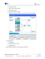
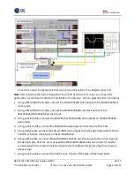
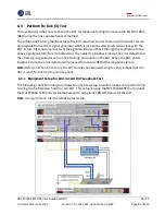
1.
Using a SMA-SMA short cable, connect the MU181000A/B clock output to the MU181500B Ext
clock input.
2.
Using a SMA-SMA short cable, connect the MU181500B jittered clock output to the
MU195020A/MU196020A Ext clock input.
3.
Using coaxial cables, connect the MU195020A/MU196020A data outputs to the MU195050A
data inputs.
4.
Using coaxial cables, connect the MU195050A data outputs to Rx Lane 0 of the CBB.
5.
Using coaxial cables, connect the MU181500B sub-rate clock outputs (100 MHz reference
clock) to the REF CLK INJ of the CBB.
6.
Using a SMA cable, connect a MU195020A/MU196020A Aux Out connector to an Aux input on
the oscilloscope.
Note the other unused MU195020A/MU196020A Aux Out connector must be
terminated with the J1632A coaxial terminator due to differential signal output (not shown in
above setup).
7.
Using phase matched cables, connect Channels 1 and 3 on the oscilloscope to the pick-off tee
input ports.
8.
Using coaxial cables, connect the CBB Tx Lane 0 to the pick-off tee tapped input ports.
9.
Using coaxial cables, connect the pick-off tee outputs to the MU195040A data inputs for
loopback error detection.
10.
Using the J1627A GND connection cable, connect the CBB to ground.
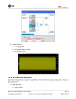
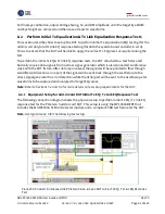
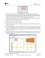
8.2.2
Equipment Setup for System Board DUT Tx Link EQ Response Test
The following connection diagram shows the physical setup to perform Tx link EQ response test
for the PCIe Gen 5 system board DUT. This setup is using the MP1900A BERT that includes the
MU195040A SI Error Detector module and a compliant CLB test fixture for the DUT.
Note
: Use logical Lane 0 for the following test setup.


