


MANUAL: 55308
REV: A
ECO: 49582
9
When subjected to elevated temperature, all
piezoelectric sensors/hardline cable systems exhibit
decreased insulation resistance, due in part to the
piezoelectric element, but due mostly to the hardline
cable necessary to withstand the high temperatures.
This situation can cause serious voltage offset
problems in direct-coupled charge amplifiers. To
solve this problem, the user must AC couple
(capacitor) the charge amplifier to the sensor/cable
system. See 5.3 Solution to Reduced Resistance , for
complete details, or use different amplifiers.
5.2 Reduced Resistance at
Charge Amplifier Input
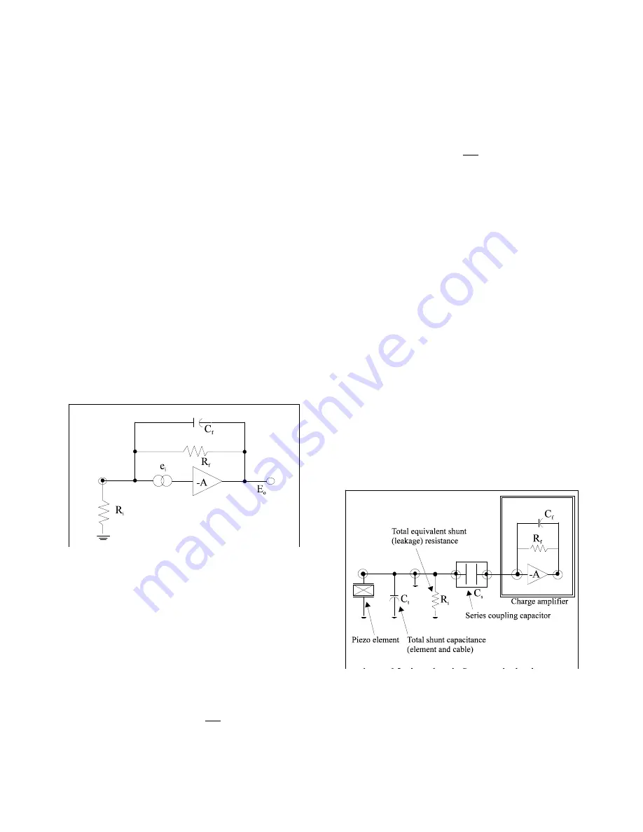
Figure 5.1 illustrates a simplified schematic of a
typical direct-coupled charge amplifier where:
R
f
= Feedback resistor (ohms)
R
i
= Input leakage resistance (ohms)
E
o
= Steady-state output voltage
(volts)
e
i
= Offset voltage: FET leakage
(volts)
C
f
= Feedback capacitor (farads)
Figure 5.1 Typical Charge Amplifier Schematic
The feedback capacitor C
f
comes into play only in
the dynamic situation and its influence does not
affect the steady-state situation. The voltage e
i
is a
DC offset voltage, usually very tiny (microvolts), that
exists at the input gate of the MOSFET circuit. This
minute leakage current exists in all real devices.
As demonstrated in Equation 1, the steady-state
(DC) output voltage E
o
is:
Equation 1
i
f
i
o
R
R
e
E
1
This equation shows that if the input (leakage)
resistance at the charge amplifier is extremely high
(approaching infinity), the output DC voltage
approaches e
i
, usually a very tiny voltage.
However, as R
i
decreases, the term
i
f
R
R
1
increases, such that the output voltage can, with
large ratios of R
f
/ R
i
, become large enough to result
in a large E
o
, perhaps large enough to be outside
the normal output voltage range of the charge
amplifier.
Because of the feedback capacitor C
f
, this output
voltage change usually does not occur rapidly but
rather, it manifests itself as a slow drift in the output
voltage level. If R
i
is low enough with respect to R
f
,
the voltage drift may continue until saturation of the
charge amplifier occurs.
5.3 Solution to Reduced
Resistance
Since the drift or offset problem is caused by a static
or steady-state imbalance at the input of the charge
amplifier, the solution involves blocking this steady-
state effect while allowing the desired dynamic
phenomena to pass. This may be accomplished by
installing a series capacitor at the input of the
charge amplifier, between the offending sensor (or
low-impedance hardline) and the input.
Figure 5.2 Piezoelectric System Block Diagram
Figure 5.2 illustrates a block diagram of the piezo-
electric system where:
C
t
= Shunt capacitor
C
s
= Series blocking capacitor


