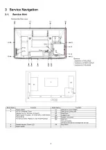


7 Disassembly and Assembly Instructions
7.1.
Remove the Rear cover
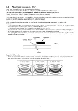
1. See Service Hint (Section 3)
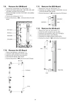
7.2.
Remove the P-Board
Caution:
To remove P.C.B. w ait 1 minute after power was off for dis
charge from electrolysis capacitors.
1. Unlock the cable clampers to free the cable
2. Disconnect the connectors (P2, P6, P7, P9, P11, P25,
P34 and P35).
3. Remove the screws (x9
and remove the P-Board.
7.3.
Remove
the
Side
terminal
cover and Rear terminal cover
1. Remove the claw (x1 ^ ) .
2. Remove the Side terminal cover.
7.4.
Remove the Tuner unit
1. Unlock the cable clampers to free the cable.
2. Disconnect the connectors (A1, A7 A11, A12 and A25).
3. Disconnect the flexible cables (A20, A31 and A32).
4. Remove the screws (x2
x1 cz|>) and remove the
Tuner unit.
3. Remove the screws (x4
х З О ) .
4. Remove the Rear terminal cover.
18
Summary of Contents for TX-PR37C10
Page 16: ...6 4 No Picture No Picture Check NG 16 ...
Page 26: ...8 1 4 Adjustment Volume Location 8 1 5 VR16600 Vad Test Point Location 26 ...
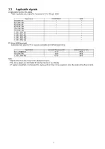
Page 31: ...9 Block Diagram 9 1 Main Block Diagram 31 ...
Page 32: ...9 2 Block 1 3 Diagram JK8302 SPEAKER L SPEAKER R SD CARD SLOT 32 ...
Page 33: ...9 3 Block 2 3 Diagram RM2501 REMOTE 33 ...
Page 36: ...10 3 Wiring 2 36 ...
Page 38: ...38 ...
Page 41: ...11 2 P Board 1 4 Schematic Diagram 40 0 ...
Page 43: ...11 4 P Board 3 4 Schematic Diagram A B C D E A P BOARD LSEP1279BEHB 3 4 F 1 2 3 4 42 ...
Page 44: ... 11 5 P Board 4 4 Schematic Diagram 10 1 11 1 12 1 13 1 14 1 15 1 16 1 17 1 18 43 ...
Page 45: ...11 6 GK К and S Board Schematic Diagram A С F 1 2 3 ...
Page 46: ...S BOARD TXN S1 ETUE ...
Page 47: ...11 7 A Board 1 21 Schematic Diagram A A A BOARD 1 21 IIC REF No 0900 0999 F 3 4 5 45 ...
Page 51: ...11 11 A Board 5 21 Schematic Diagram 37 38 39 40 ...
Page 52: ...А A BOARD 5 21 ADV_V REF No 4500 4799 41 42 43 44 45 49 ...
Page 53: ...11 12 A Board 6 21 Schematic Diagram TO 6 71 46 47 48 49 50 50 ...
Page 54: ...А A BOARD 6 21 ADV_A REF No 2000 2499 51 52 53 54 ...
Page 55: ...11 13 A Board 7 21 Schematic Diagram 55 56 57 58 59 60 61 62 63 51 ...
Page 57: ...ТО 9 21 ТО 7 21 68 69 70 71 72 52 ...
Page 61: ...11 18 A Board 12 21 Schematic Diagram 100 101 102 103 104 105 106 107 108 56 ...
Page 63: ...11 20 A Board 14 21 Schematic Diagram DO W N LEFT 118 119 120 121 122 123 124 125 126 58 ...
Page 68: ...11 25 A Board 19 21 Schematic Diagram A A BOARD 19 21 DTV CRNo 8300 8999 163 164 165 166 ...
Page 69: ...63 ...
Page 74: ...11 30 C2 Board 1 2 Schematic Diagram A C2 BOARD TNPA4891 1 2 TO A BOARD A31 C21 л B 68 ...
Page 75: ...11 31 C2 Board 2 2 Schematic Diagram TO A BOARD A32 10 11 12 13 14 15 16 17 18 69 ...
Page 76: ...11 32 SC Board 1 3 Schematic Diagram в D A SC BOARD TXNSC1 ERUE 1 3 1 2 3 4 ...
Page 77: ...IC16771 C0CBADC00072 70 ...
Page 78: ...11 33 SC Board 2 3 Schematic Diagram 10 11 12 13 14 15 16 17 18 71 ...
Page 79: ...11 34 SC Board 3 3 Schematic Diagram 19 20 21 22 23 24 25 26 27 72 ...
Page 80: ...11 35 SS Board 1 2 Schematic Diagram A B C D E F 3 4 5 73 ...
Page 85: ...P BOARD COMPONENT SIDE LSEP1279BEHB 77 ...
Page 87: ...K BOARD FOIL SIDE TXN K1ETUE K BOARD COMPONENT SIDE TXN K1 ETUE ...
Page 88: ...12 3 A Board A BOARD FOIL SIDE A PR37C10 6 5 4 3 2 1 A I B I C I D I E I F I G I H I I 79 ...
Page 91: ...A BOARD COMPONENT SIDE A PR37C10 81 ...
Page 94: ...12 6 SC Board SC BOARD FOIL SIDE TXNSC1ERUE 6 5 4 3 2 1 A I B I C I D I E I F I G I H I I 84 ...
Page 97: ...SC BOARD COMPONENT SIDE TXNSC1ERUE B G 6 5 4 3 2 1 E F H 86 ...
Page 100: ......
Page 102: ...13 1 2 Packing 1 90 ...
Page 103: ...91 ...


