


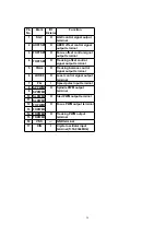

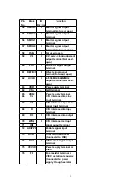


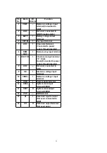
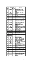
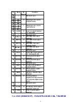

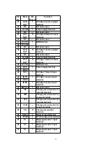


Pin
No.
Mark
I/O
Division
Function
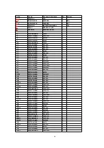
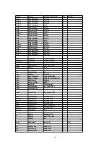
1
VREF-
—
Reference voltage- input
terminal (Connected to
GND)
2
AN0
—
Not used, connected to
GND through resistor
3
BATT
I
Battery voltage detect
terminal
4
KEY IN
I
Key input terminal
5
AN3
I
Area select termianl
(Connected to power
supply through resistor)
6
REM
KEY
I
Remocon key input terminal
7
DOCTOR
I
Check mode input terminal
(“L”:check
mode)(Connected to power
supply through resistor)
8
AN6
—
Not used, connected to
GND
9
SE
I
Sled error voltage input
terminal
10
VREF+
I
Reference input
terminal
11
VDD
I
Power supply terminal
12
OSC2
I
System clock input
terminal (8MHz)
13
OSC1
O
System clock output
terminal (8MHz)
14
VSS
—
GND terminal
15
XI
I
Sub clock input terminal
(Not used, connected to
GND)
16
XO
O
Sub clock output terminal
(Not used, open)
31
Summary of Contents for SJ-MJ70
Page 5: ...5 ...
Page 6: ...6 ...
Page 7: ...7 ...
Page 14: ...4 When entering the main unit s key check mode KEY will be displayed 14 ...
Page 16: ...16 ...
Page 17: ...17 ...
Page 18: ...18 ...
Page 19: ...19 ...
Page 20: ...20 ...
Page 41: ...C309 11 ECUENC333KBQ 16V 0 033U 3 41 ...
Page 45: ...45 ...
Page 49: ......
Page 50: ......
Page 51: ......
Page 52: ......
Page 53: ......
Page 54: ......
Page 55: ......
Page 56: ......
Page 57: ......
Page 58: ......
Page 59: ......
Page 60: ......
Page 61: ......
Page 62: ......
Page 63: ......
Page 64: ......
Page 65: ......
Page 66: ......