background image

4 Handling the Lead-free Solder

4.1. Service caution based on legal restrictions

4.1.1. General description about Lead Free Solder (PbF)

The lead free solder has been used in the mounting process of all electrical components on the printed circuit boards used for this
equipment in considering the globally environmental conservation.

The normal solder is the alloy of tin (Sn) and lead (Pb). On the other hand, the lead free solder is the alloy mainly consists of tin
(Sn), silver (Ag) and Copper (Cu), and the melting point of the lead free solder is higher approx.30 degrees C (86°F) more than that
of the normal solder.

Definition of PCB Lead Free Solder being used

The letter of “PbF” is printed either foil side or components side on the PCB using the lead free solder.
(See right figure)

Service caution for repair work using Lead Free Solder (PbF)


·


The lead free solder has to be used when repairing the equipment for which the lead free solder is used.

(Definition: The letter of “PbF” is printed on the PCB using the lead free solder.)


·


To put lead free solder, it should be well molten and mixed with the original lead free solder.


·


Remove the remaining lead free solder on the PCB cleanly for soldering of the new IC.


·


Since the melting point of the lead free solder is higher than that of the normal lead solder, it takes the longer time to melt
the lead free solder.


·


Use the soldering iron (more than 70W) equipped with the temperature control after setting the temperature at 350±30
degrees C (662±86°F).

Recommended Lead Free Solder (Service Parts Route.)


·


The following 3 types of lead free solder are available through the service parts route.

RFKZ03D01K-----------(0.3mm 100g Reel)
RFKZ06D01K-----------(0.6mm 100g Reel)
RFKZ10D01K-----------(1.0mm 100g Reel)

Note

* Ingredient: Tin (Sn), 96.5%, Silver (Ag) 3.0%, Copper (Cu) 0.5%, Cobalt (Co) / Germanium (Ge) 0.1 to 0.3%

7

SH-FX85P / SH-FX85PC

Summary of Contents for SH-FX85P

Page 1: ...FX85TPP SB FX85P SB FX85PC Colour K Black Type 106 Hz 22 kHz 10 dB n GENERAL Power supply AC 120 V 60Hz Power consumption Digital transmitter 1 7 W Wireless sound system 38 W Dimensions W x H x D Digital transmitter 65 mm x 52 mm x 8 6 mm 2 9 16 x 2 1 16 x 11 32 Wireless sound system 430 mm x 170 5 mm x 189 mm 16 15 16 x 6 23 32 x 7 6 16 Mass Digital transmitter 0 02 kg 0 04 lbs Wireless sound sys...

Page 2: ...igital Receiver SB FX85P PC 25 10 5 Disassembly of Transmitter Module P C B SH FX85T 37 11 Service Positions 38 11 1 Checking of Panel RF Adapter and Receiver Module P C B 38 11 2 Checking of D Amp and D Port P C B 39 12 Voltage Measurement Waveform Chart 40 12 1 Voltage Measurement 40 12 2 Waveform Chart 42 13 Wiring Connection Diagram 43 14 Block Diagram 45 14 1 DIGITAL AMPLIFIER D PORT PANEL BL...

Page 3: ...on Breakdown Note The table below show the breakdown for the digital transmitter and wireless system table 1 Digital Tx Rx System SH FX85P PC K Digital Transmitter SH FX85TPP K Digital Receiver SB FX85P PC K 3 SH FX85P SH FX85PC ...

Page 4: ...should be between 1MΩ and 5 2Ω When the exposed metal does not have a return path to the chassis the reading must be 2 1 2 LEAKAGE CURRENT HOT CHECK See Figure 1 1 Plug the AC cord directly into the AC outlet Do not use an isolation transformer for this check 2 Connect a 1 5kΩ 10 watts resistor in parallel with a 0 15µF capacitors between each exposed metallic part on the set and a good earth grou...

Page 5: ... correct it 3 Turn on the power once again after one minute Note When the protection circuitry functions the unit will not operate unless the power is first turned off and then on again 2 4 Safety Part Information Safety Parts List There are special components used in this equipment which are important for safety These parts are marked by in the Schematic Diagrams Replacement Parts List It is esse...

Page 6: ...y 3 Use only a grounded tip soldering iron to solder or unsolder ES devices 4 Use only an anti static solder removal device Some solder removal devices not classified as anti static ESD protected can generate electrical charge to damage ES devices 5 Do not use freon propelled chemicals These can generate electrical charges sufficient to damage ES devices 6 Do not remove a replacement ES device fro...

Page 7: ...k using Lead Free Solder PbF The lead free solder has to be used when repairing the equipment for which the lead free solder is used Definition The letter of PbF is printed on the PCB using the lead free solder To put lead free solder it should be well molten and mixed with the original lead free solder Remove the remaining lead free solder on the PCB cleanly for soldering of the new IC Since the ...

Page 8: ...5 Accessories Note Refer to Packing Materials Accessories Parts List Section 22 for the part number 8 SH FX85P SH FX85PC ...

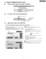
Page 9: ...6 Using of Digital Receiver Unit 6 1 Connecting the digital transmitter SH FX85T 6 2 AC Power Cord connection SB FX85 6 3 Making the wireless link SB FX85 9 SH FX85P SH FX85PC ...

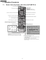
Page 10: ...list Return to previous screen or show the setup menu Select the disc or show disc information Turn the unit off automatically Sleep timer 1 Press and hold the button 2 While the time is shown press the button repeatedly to select the time in minutes The maximum setting is 120 min in 30 min steps Press and hold the button again to confirm the remaining time on the unit s display Start up and play ...

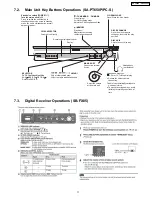
Page 11: ...main unit TUNING Headphone plug type 3 5 mm 1 8 stereo mini plug Reduce the volume before connecting Audio is automatically switched to 2 channel stereo To prevent hearing damage avoid listening for prolonged periods of time OPEN CLOSE Open Close the disc drawer TUNE MODE FM MODE Stop playing Select the tuning mode Adjust the FM reception condition Play discs Memorize the receivng i radio stations...

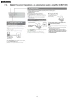
Page 12: ...7 4 Digital Receiver Operations as stand alone audio amplifier SB FX85 12 SH FX85P SH FX85PC ...

Page 13: ... multi room function wherein it operates as a second room wireless receiver up to a maximum of two Maximum range attainable is 30 meters It can send commands to the main unit to control functions such as Play Stop Forward Skip Channel Up Reverse Skip Channel Down It also has a built in DAP pocket for stand alone operation by inserting a DAP device e g iPod in the DAP pocket to play the device only...

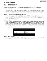
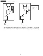
Page 14: ...transmitter uses one ADC Analog to Digital Converter and transmits audio through Channel 2 Type 1 receiver Rx uses one DAC and output audio through Channel 2 The firmware that is downloaded to EEPROM IC multiplexes which channel to listen to in this case Channel 2 since type A is transmitting from channel 2 In by setting the baseband accordingly 14 SH FX85P SH FX85PC ...

Page 15: ...5 Wireless feature is enabled by default when the user uses transmitter type B 8 1 4 LED Indication For FX65 FX66 there will be two color LED that will be used to indicate Power On and Link If link the two color LED will be green else it will be red For FX85 the front panel will have LED indicators for Standby Wireless Link Charge Option and Music Port During Power On Standby LED will be OFF Only ...

Page 16: ...is period elapsed the transmitter will revert back to using close connect code whereby only those receivers which have the same ID as the transmitter will be able to link The user also has the option to exit the ID setting operation by pressing the same keys iPod Detection and Charging iPod is detected once inserted on the FX85 and battery charging automatically starts The iPod Charging in Standby...

Page 17: ...s able to send audio signal for second room via Ch 1 and first room via Ch 2 In this configuration streams AB is used to transmit the audio from main unit to the first room Type 1 receiver FX65 FX66 via Ch 2 While the second room audio is transmitted through stream CD via Ch 1 Multi room Multi source TX RX RX FX65 FX66 FX85 CH1 CD CH2 AB B 1 1 Case 3 A Wireless Subwoofer This configuration Type A ...

Page 18: ...eiver FX65 FX66 through streams AB via Ch 2 and Type 2 second room receiver FX85 comes from transmitter B through streams CD via Ch 1 For this configuration the user must perform ID setting for FX85 if it is sold as an accessory but for bundled type it already is paired with the transmitter RX RX RX RX CH2 AB CH2 AB CH1 CD B 1 1 1 Multi room Multi source 18 SH FX85P SH FX85PC ...

Page 19: ...cted baseband IC settings Not all baseband register settings a total of 512 bytes will be read from the EEPROM IC though Aside from getting the baseband settings from the EEPROM IC it is also used to enable FCC testing select the application type and entering into doctor mode this can be enabled also by sending a command via the main unit 8 1 9 Doctor Mode For normal operation but automatic freque...

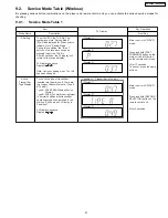
Page 20: ...king Player buttons Remote control unit buttons Application Note FAST FORWARD 3 ID setting Refer to the section 9 2 1 for more information SECOND SELECTOR press hold Active transmitter display STOP only in AUX 4 RF channel 1 display Refer to the section 9 2 2 for more information 5 RF channel 2 display 6 RF channel 3 display 7 Auto RF channel display Note Main room refers to the location of the ma...

Page 21: ...ss and hold SECOND SELECTOR button on the remote control unit To set the ID in the Tx Rx The system goes into Pairing Mode P will be displayed for 60 seconds to indicate it is in Pairing Mode During this condition the ID set button on the receiver unit can be pressed to pair the Tx Rx After 60 seconds the FL display will return to its previous display FL Display sequence Display 1 2 3 Note Carry o...

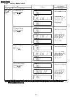
Page 22: ...annels 1 2 or 3 RF channel channels 1 2 or 3 After 2 seconds Display 1 Display 2 Display 3 After 2 seconds Main room is in AUX mode Main room is in AUX mode Main room is in AUX mode Main room is in AUX mode Press and hold STOP button on the main unit and 4 button on the remote control unit Press and hold STOP button on the main unit and 5 button on the remote control unit After 2 seconds Press and...

Page 23: ...elow is the list of disassembly sections Disassembly of Net frame assembly Disassembly of Panel P C B Disassembly of Woofer 1 Disassembly of Woofer 2 Disassembly of Bottom Chassis Unit Disassembly of SMPS Module Unit Disassembly of D Amp P C B Disassembly of Receiver Module P C B Disassembly of D Port P C B Disassembly of RF Adapter P C B Disassembly of Transmitter Module P C B SH FX85T 10 1 1 SMP...

Page 24: ...e procedure for disassembling the casing and inside parts for internal inspection when carrying out the servicing For the digital receiver unit only To assemble the unit reverse the steps shown in the chart below 10 3 Main Parts Location Diagram 24 SH FX85P SH FX85PC ...

Page 25: ...y of Net frame assembly Step 1 Insert a steel rule between net frame assembly and speaker box Step 2 Push up the steel rule as arrow shown Step 3 Push up the steel rule along the sides of speaker box as shown Step 4 Remove the net frame assembly 25 SH FX85P SH FX85PC ...

Page 26: ...to step 4 in item 10 4 1 Step 1 Remove 4 net catchers Step 2 Remove 10 screws Step 3 Insert the steel rule between front cabinet and speaker box Step 4 Push up the steel rule along the sides of speaker box slowly as arrow shown 26 SH FX85P SH FX85PC ...

Page 27: ...h the front cabinet as arrow shown Step 6 Detach gray blue wires Step 7 Detach red black wires Step 8 Detach cable CN1000 Step 9 Remove the power button and volume knob Step 10 Remove 4 screws 27 SH FX85P SH FX85PC ...

Page 28: ... item 10 4 1 Follow step 1 to step 8 in item 10 4 2 Step 1 Remove 4 screws Step 2 Remove woofer 1 as arrow shown 10 4 4 Disassembly of Woofer 2 Follow step 1 to step 4 in item 10 4 1 Follow step 1 to step 8 in item 10 4 2 Step 1 Remove 4 screws Step 2 Remove woofer 2 as arrow shown 28 SH FX85P SH FX85PC ...

Page 29: ...enna as arrow shown Step 2 Remove 5 screws Step 3 Upset the unit Caution Place the unit on a cushion to avoid damage to the antenna Step 4 Remove 1 screw Step 5 Detach rear panel unit as arrow shown Step 6 Detach cables CN1005 CN1002 and CN1007 29 SH FX85P SH FX85PC ...

Page 30: ...to step 6 in item 10 4 5 Step 1 Remove 1 screw Step 2 Release the catches and detach the rear panel unit as arrow shown Step 3 Position the rear panel unit as arrow shown Step 4 Detach cable CN2 on SMPS Module Step 5 Remove 3 screws 30 SH FX85P SH FX85PC ...

Page 31: ...MPS module unit is under the clutch when placing back the SMPS module unit to the rear panel unit 10 4 7 Disassembly of D AMP P C B Follow step 1 to step 6 in item 10 4 5 Follow step 1 to step 3 in item 10 4 6 Step 1 Detach cables CN1001 and CN2 31 SH FX85P SH FX85PC ...

Page 32: ...able from Receiver Module P C B using service jig Step 3 Remove 3 screws Step 4 Remove the D Amp P C B as arrow shown Replacement of Digital Amp IC IC5200 Step 1 Release the heat sink clip as arrow shown 32 SH FX85P SH FX85PC ...

Page 33: ... the IC5200 as arrow shown 10 4 8 Disassembly of Receiver Module P C B Follow step 1 to step 6 in item 10 4 5 Follow step 2 in item 10 4 7 Step 1 Push the both sides of P C B holders as arrow shown Step 2 Remove the Receiver Module P C B as arrow shown 33 SH FX85P SH FX85PC ...

Page 34: ... of the other side of Receiver Module P C B Step 6 Flip over the Receiver Module P C B Step 7 Remove the shield plate as arrow shown Cautions 1 Ensure that the metal plate is facing outwards when placing back the Receiver module P C B 2 Ensure to fix the shield plate by aligning the locating pins of shield plate into holes of Receiver Module P C B 34 SH FX85P SH FX85PC ...

Page 35: ... P C B Follow step 1 to step 6 in item 10 4 5 Follow step 1 to step 3 in item 10 4 6 Step 1 Detach the connector CN1001 Step 2 Remove 1 screw Step 3 Release the catch to remove the D Port P C B as arrow shown 35 SH FX85P SH FX85PC ...

Page 36: ...tep 1 to step 6 in item 10 4 5 Follow step 1 to step 3 in item 10 4 6 Step 1 Detach coaxial cable from RF Adapter P C B using service jig Step 2 Remove RF Adapter P C B by desoldering the connecting points Step 3 Remove 1 screw 36 SH FX85P SH FX85PC ...

Page 37: ...10 5 Disassembly of Transmitter Module P C B SH FX85T Step 1 Remove 4 screws Step 2 Remove bottom casing as arrow shown 37 SH FX85P SH FX85PC ...

Page 38: ...11 Service Positions Note For description of the disassembly procedures see the Section 10 11 1 Checking of Panel RF Adapter and Receiver Module P C B 38 SH FX85P SH FX85PC ...

Page 39: ...11 2 Checking of D Amp and D Port P C B 39 SH FX85P SH FX85PC ...

Page 40: ...er Circuit voltage and waveform described herein shall be regarded as reference information when probing defect point because it may differ from actual measuring value due to difference of Measuring instrument and its measuring condition and product itself 12 1 Voltage Measurement 12 1 1 D AMP P C B 4GH 0Q 1 2 56 0 4GH 0Q 1 2 56 0 4GH 0Q 1 2 56 0 4GH 0Q 1 2 56 0 4GH 0Q 1 2 56 0 4GH 0Q 1 2 56 0 4GH...

Page 41: ...12 1 3 PANEL P C B 4GH 0Q 1 2 56 0 5 2 2 2 0 2 2 0 2 3 3 3 3 3 41 SH FX85P SH FX85PC ...

Page 42: ...12 2 Waveform Chart RF TEST POINT PLAY 42 SH FX85P SH FX85PC ...

Page 43: ...0 I D SET SOLDER SIDE PbF RF ADAPTER P C B D PANEL P C B B SOLDER SIDE PbF CN1000 1 16 VR1000 RECEIVER MODULE P C B E SOLDER SIDE PbF TRANSMITTER MODULE P C B F 1 2 23 24 SOLDER SIDE PbF CN1001 1 12 CN1002 JK1000 Z1000 SPEAKER WOOFER SIDE A 1 21 2 22 CN1 SOLDER SIDE PbF D PORT P C B C CN3 CN2 CN2 CN3 CN3 TO SMPS MODULE TO MAIN UNIT X Coaxial Cable X 43 SH FX85P SH FX85PC ...

Page 44: ...SH FX85P SH FX85PC 44 ...

Page 45: ... 0 0 0 0 4 8 4 8 4 8 4 8 4 8 3 3 3 3 3 41 4 41 4 61 61 8552 8552 176 116 176 116 8 2 8 2 15 8UU 8UU 2146A 2146A4 2146A4 2146A 2146A 2146A4 2146A4 2146A 8UU2 1 0 855 6 55 2 2416 56 8 8 0 855 855 0 0 0276 56 0276 56 76 76 29 1 7 614 29 1 7 614 0 4 15 614 1 56 6 2 4 674 5 0514 744 06 2416 6 10 81 6 2416 6 10 10641 0 0 5 10641 0 0 5 4 8 4 8552 8 2 4 8 4 19 4 8 4 4 8 4 19 5 0 0 5 0 5 0 0 2146A 2146A4 2...

Page 46: ... 6 6 A 6 A A3 2 2 2 2 2 8 2 106 A 6 76 52A5 52A5 21 A 6 6 0 5 6 2 2 5 5 5 8 2 456 8176 8 0 84 8 4 7 614 6 8 4 7 614 0 1 8 4 7 614 4 0 6 A 6 A 6 A 6 A A016 6 A 6 A3 6 A 6 A3A016 A4 2 A4 0 A4 30 A4 32 7 1A A176 4 8 4 7 614 8 A4 8 8 176A 10641 75 10641 75 8 5722 8 0 8176 8176 0 8 0 8 8 2 8 8 8 8 8 8 2 112 6 4 8 A4 A 8 A4 A8 84 84 8 A4 A 84 84 84 8 A 0 8 A2 84 84 84 84 8 A6 A2 4 2 8 A2 8 A6 A 8 A 2 84...

Page 47: ...9 6 10641 6 0276 06 00 5 6 06 00 5 6 06 8 06 2 06 2 06 2 2 2 A 10 5 5 5 6 A 6 A 06 06 6 A A3 6 A 6 A 6 A A3 2 5 5 5 8 2 2 456 8176 8 0 84 6 4 7 614 0 1 4 7 614 4 4 7 614 0 6 A 6 A 6 A 6 A A016 6 A 6 A3 6 A 6 A3A016 A4 2 A4 0 A4 30 A4 32 7 1A A176 4A 8 0A 10641 75 10641 75 8 5722 8 0 8176 8176 0 8 0 8 8 8 8 8 8 3 8 8 8 8 2 112 6 4 8 A4 A 8 A4 A8 84 84 8 A4 A 84 84 84 8 A 0 8 A2 84 84 84 84 8 A6 A2 ...

Page 48: ...SH FX85P SH FX85PC 48 ...

Page 49: ...rs etc are used When replacing any of components be sure to use only manufacturer s specified parts shown in the parts list Capacitor values are in microfarad µF unless specified otherwise F Farad pF Pico Farad Resistance values are in ohm Ω unless specified otherwise 1K 1 000Ω 1M 1 000KΩ Voltage and Signal lines B signal line B signal line Main signal line RF signal line Special Note This model u...

Page 50: ...50 SH FX85P SH FX85PC ...

Page 51: ... 0 18 C1523 0 18 0 18 C1521 C1512 0 18 C1522 0 18 C1409 0 1 C1422 1 R1000 47K C1000 0 C1009 6 3V820 3 2 1 K4CZ01000027 Z1000 C2000 0 1 R2003 47 2 7K R2004 100K R1005 Q1003 B1ACKD000006 REGULATOR D1001 B0ECKP000002 0 1 C1003 Q1009 B1GBCFJJ0051 PCONT SWITCH D2000 B0BC9R000008 R1020 27K VR_LCH_IN DPORT_LCH CHARGE_LED OPTION_LED AGND 8 4V 5V_GND MPORT_LED WIRELESS_LED PCONT_LED 5V VR_RCH_IN MPORT_LCH ...

Page 52: ...6 0 1 C5602 16V10 R1013 120K C5215 0 1 5 6K R5208 330p C5216 R5204 1 5K C5233 0 1 C5231 1000p C5220 0 1 R5207 5 6K 0 1 C5214 C5232 0 1 C5205 220p 0 1 C5219 1000p C5234 C5200 0 1 C5201 0 015 C5212 220p C5202 0 22 19 21 23 22 20 10 2 1 8 9 7 4 5 6 3 12 15 14 17 18 16 13 11 IC5200 C1AA00000755 CLASS D DIGITAL AMPLIFIER IC 0 1 C5213 C5203 220p R5200 10 C5211 220p C5522 0 1 R1002 1 2K C1004 35V1000 L10...

Page 53: ...J0051 LED SWITCH 0 R1112 0 R1111 S1200 PLAY S1202 CH FWD S1203 CH RWD S1204 SELECTOR 6 3 4 1 S1000 POWER BUTTON S1201 STOP 6 7 5 2 4 3 8 1 IC1300 C0ABBB000067 OP AMP IC R1200 2 2K R1204 1K R1203 1K R1201 1 8K R1202 1 2K R1101 270 5V LINK_LED 5V_GND D1101 B3ABA0000397 WIRELESS LINK LED GREEN CHARGE_LED WIRELESS_LED KEY OPTION_LED MPORT_LED 5V_GND 5V AGND 8 4V AGND LINK_LED KEY CHARGE_LED WIRELESS_L...

Page 54: ...1004 15 R1006 1K R1005 3 9K 5V_GND C1014 0 1 5V C1110 470P 1 7 6 4 2 3 5 JK1000 MUSIC PORT OPTION V 1 TO DOCK 4 7K R1211 MPORT_RCH R1111 4 7K C1210 470P D GND AGND AGND AGND 5V D GND OUT STDBY INV VCC VBUS VIDEO BATT2 V_GND LCH_IN DPORT_LCH RESERVE BATT_GND MIC_L RF_DETECT CHARGE_CTRL IPOD_DET RCH_IN DLINKDET1 UART_IN DLINKDET2 RCH_OUT UART_OUT IPOD_DETECT AD_CNTL RF_SEL MIC_VCC RF_MUTE ANT MIC_GN...

Page 55: ...E LINK CONNECT LDO KEY LED_DSPLY1_TXD CHARGE_CONTROL DC_DET GND IPOD_DETECT JOGB LED_DSPLY3 5V 6 3V100 C1112 CH2_L_OUT AGND AGND TP21 5VSUPPLY CH2_R_OUT 5VSUPPLY JOGA PCONT GND R1106 0 0 1 C1111 R1107 0 4 2 1 3 5 IC1102 C0CBCBC00090 3 3V REGULATOR R1112 0 C19 6 3V100 ASP_SI ASP_SC LED_DSPLY2_RXD 5VSUPPLY R1113 0 6 5 8 9 11 12 10 18 15 17 16 20 19 13 14 7 2 1 4 3 22 21 CN1 PATTERN CONNECTOR C51 0 1...

Page 56: ... R1407 0 R1410 0 SD_OUT_B 7 5 6 1 2 4 3 10 9 12 14 15 16 13 11 8 IC1400 C0FBBK000066 DAC R1405 0 R1403 47K CH2_R_OUT R1401 1K CH2_L_OUT VSS VDD D1F1 VCOM MCLK PDN BICK LRCK SDTI TEST NC NC VOUT VIN VSS NC GND VCC WP SCL SDA DEM DFSI DFS0 D1F0 ROUT LOUT 3 3V 3 3V 3 3V 15 16 17 18 19 20 21 22 23 24 25 26 27 28 A B D E F H G C SCHEMATIC DIAGRAM 6 SH FX85P PC SB FX85P PC RECEIVER MODULE CIRCUIT STATIC...

Page 57: ...7 16 17 14 15 18 13 24 20 22 21 19 23 IC13 C1CB00002648 RF IC R1 G1C2N7ZA0068 RF_TEST_POINT RF_TEST_POINT 2 3 1 5 4 C40 2 2p C43 15p 9 12 10 11 7 6 5 4 3 8 2 1 IC1 IC1 C1CB00001841 TRANSFER SWITCH IC C45 10p C44 10p CN2 PCB ANT B1 VRX_BB_I BYPASS B4 VCC_CP XTAL VCC_VCO GND_CP TUNE GND_VCO RX_BB_Q RX_BB_Q CP_OUT VCC_XTAL GND_XTAL VRX_BB_I RX TX ANT1 V1 ANT2 V2 CLOCKOUT RX_HP LD VCC_RX_VGA B6 ANT2 V...

Page 58: ...IC10 C1AB00002772 BASE BAND IC BB_RXIP XTAL_2 VCC2_IO REFP BB_RXIN XTAL_1 VCM GPIO_0 CON SDA A0 AGND_IO VCC_3_IO AUDIO_CLK_OUT A1 GPIO_RESN SCL GPIO_3 DBG_TXD GPIO_1 FRM_CLK GPIO_2 INT RSET B4 BB_RXQN BB_RXQP LRCK DIN_B BCK DIN_A DOUT_B DOUT_A VCC2_A GND_A REFN VCC3A_ADC GND_IO TMO GND_A GND_K VCC3A_REG VCC_K TX_ANT_A_EN TX_DATA_I TX_ANT_C_EN TX_DATA_I_NOT B2 SHDN SPI_EN SPI_CLK VCC_3_IO B5_MODE_P...

Page 59: ...11 10 2 3 4 1 7 8 6 5 17 19 21 23 26 25 29 28 30 27 24 22 20 18 15 16 IC1000 C2BBED000056 MCU IC CH2_L_IN CH1_R_IN AGND LDO SCLKIN 5VSUPPLY CH2_R_IN AGND SDIN SDOUT 5V 6 3V100 C1112 AGND AGND TP21 5VSUPPLY AGND GND AGND CH1_L_IN R1106 J0JCC0000278 0 1u C1111 R1107 0 4 2 1 3 5 IC1102 C0DBZGC00067 3 3V REGULATOR R1112 0 C19 6 3V100 5VSUPPLY R1114 0 6 5 8 9 11 12 10 18 15 17 16 20 19 13 14 7 2 1 4 3 ...

Page 60: ...2_R_IN SCLK SCLKIN SDIN C1301 10V22 C1305 10V22 R1305 0 R1306 0 C1306 0 1 10V22 C1307 C1308 0 1 C1303 10V22 C1302 10V22 R1301 1K R1302 1K R1303 47K R1304 47K C1304 0 1 7 5 6 1 2 4 3 10 12 14 15 16 13 11 8 9 IC1300 C0FBAK000019 ADC DIF PDN MCLK CKS2 SDTO SCLK LRCK CKS0 VCOM CKS1 VD VA AGND DGND AINL AINR 3 3V 3 3V 3 3V 3 3V R1111 47K R1110 27K R1109 10K R1108 10K SDOUT 5VSUPPLY Q1101 B1GBCFJJ0051 L...

Page 61: ...36 34 33 35 29 26 25 27 16 17 14 15 18 13 24 20 22 21 19 23 IC13 C1CB00002648 RF IC R6 G1C2N7ZA0068 R1 G1C2N7ZA0068 2 3 1 5 4 2 3 1 5 4 C40 2 2p C43 15p 9 12 10 11 7 6 5 4 3 8 2 1 IC1 IC1 C1CB00001841 TRANSMITTER SWITCH IC C45 10p C44 10p B1 VRX_BB_I BYPASS B4 VCC_CP XTAL VCC_VCO GND_CP TUNE GND_VCO RX_BB_Q RX_BB_Q CP_OUT VCC_XTAL GND_XTAL VRX_BB_I RX TX ANT1 V1 ANT2 V2 CLOCKOUT RX_HP LD VCC_RX_VG...

Page 62: ...1 59 60 IC10 C1AB00002772 BASE BAND IC BB_RXIP XTAL_2 VCC2_IO REFP BB_RXIN XTAL_1 VCM GPIO_0 CON SDA A0 AGND_IO VCC_3_IO AUDIO_CLK_OUT A1_TM_SEL0 GPIO_RESN SCL GPIO_3 DBG_TXD GPIO_1 FRM_CLK GPIO_2 INT RSET B4 BB_RXQN BB_RXQP LRCK DIN_B BCK DIN_A DOUT_B DOUT_A VCC2_A GND_A REFN VCC3A_ADC GND_IO TMO GND_A GND_K VCC3A_REG VCC_K TX_ANT_A_EN TX_DATA_I TX_ANT_C_EN TX_DATA_I_NOT B2 SHDN SPI_EN SPI_CLK VC...

Page 63: ...1 R1522 C1511 R1514 C1513 R1511 C1523 R1513 R1512 C1521 C1512 C1522 K5202 K5200 K5234 K5231 K5232 C1442 C1441 R1005 R1006 D1002 R1021 D1003 R1022 D1004 D1005 R1431 C1416 C1417 C1415 W1075 R1024 C1109 R1404 R1403 R1402 R1401 C1401 C1402 C1405 C1403 C1404 IC1400 C55 C54 C53 C17 R1506 R1505 R1504 R1503 R1502 R1501 R1500 C56 C1108 C1110 C26 R1 IC1102 IC13 C36 C9 C12 C20 C18 C58 R41 C21 C66 C65 C33 L21...

Page 64: ...0 C1019 R1017 D1000 OPTION V I TO DOCK L1002 C1011 L1000 JK1000 C1015 CN1001 SIDE A SIDE B SIDE A SIDE B R1200 R1201 R1202 R1103 R1104 Q1103 R1105 R1102 Q1102 R1114 R1112 R1203 R1113 Q1101 R1101 R1111 R1115 R1204 Q1105 W1101 Q1104 W1102 W1103 W1104 C1511 C1512 C1521 C1522 R1514 R1521 R1522 R1524 R1320 R1511 R1512 R1310 C1437 C1438 IC1300 W1105 C1525 C1322 C1323 R1520 C1313 R1525 C1312 C1515 R1510 ...

Page 65: ... R26 R19 R1016 C1008 C1009 R1107 R1112 R1108 R1006 R1109 R1007 D1101 R1012 R1018 C25 C1111 R1106 C1103 C1102 C32 R43 C31 C3 C70 R1102 R1101 IC3 D1102 C1004 C1101 R39 R38 C1112 R1014 R1022 C1001 C1114 C1113 R1104 R1002 R1001 R1013 R1017 R1005 R1003 R1021 R1020 R1019 R1004 R1009 R1105 R1103 IC1105 IC1103 IC1000 R11 R25 R27 R18 R22 R10 R13 R7 R9 C47 R8 C60 R15 C49 R46 C46 C48 C1005 W1 W4 W3 Y1 R1115 ...

Page 66: ...SH FX85P SH FX85PC 66 ...

Page 67: ... B0ECKP000002 B0ACCK000005 B0ACCE000003 B1ADCE000012 B1GBCFJJ0051 B1ABCF000176 E B C C1CB00002648 48P C1CB00001841 12P C1BB00001071 1 4 8 5 C0ABBB000067 1 C1AB00002772 64P B C E B1ACKD000006 B3ABA0000397 B3AAA0000803 B C E B1BACG000023 Anode Cathode A Ca C1AA00000755 1 22 2 23 C0DBAZG00033 B0BC9R000008 A Ca Cathode Anode No 1 A Ca Cathode Anode B0JCPD000025 67 SH FX85P SH FX85PC ...

Page 68: ...erminal Name I O Function 48 TX_DATA_ I_NOT O BB I channel transmit data complement 49 TX_DATA_Q O BB Q channel transmit data 50 TX_DATA_ Q_NOT O BB Q channel transmit data complement 51 RXHP O RF transceiver control 52 V25 2 5V Power Supply Output of internal voltage regulator fed by external 3 3V connection 53 VCC3_AREG 3 3V input for internal 2 5V regulator 54 GND_A Ground connection 55 GND_A_D...

Page 69: ...downconverter 47 ANT_SEL GND connection 48 CPRXTX I Transmit and Receiver mode selection 19 3 IC1000 C2BBYY000375 IC MCU Pin NO Terminal Name I O Function 1 P2 1 No Connection 2 P2 0 O Port 2 mode LDO 3 P0 1 O Port 0 mode LINK 4 P0 0 O Port 0 mode PCONT 5 P12 0 I Potential input for external low voltage detection 6 RST I System reset input 7 FLMD0 Flash memory programming mode setting 8 EXCLK I Ex...

Page 70: ...70 SH FX85P SH FX85PC ...

Page 71: ...20 Exploded Views 20 1 Cabinet Parts Location SH FX85P SH FX85PC 71 ...

Page 72: ...20 2 Packaging SH FX85P SH FX85PC 72 ...
Page 73: ... by PAVCSG Table 1 21 1 TX RX KIT ASSEMBLY TX RX kit assembly consists of the transmitter card Tx Module with casing and the Rx Module P C B Note Pls carry out pairing for ID setting Refer to section 9 2 of this document on procedures 21 2 TX CASE ASSEMBLY TX card assembly consists of the Tx Module P C B in assembled condition with top bottom casing Note Pls carry out pairing for ID setting Refer ...

Page 74: ...R M IC1000 C2BBYY000375 IC MCU M IC1102 C0CBCBC00090 IC 3 3V LDO M IC1103 C0CBCBC00090 IC 3 3V LDO M IC1105 C1BB00001071 IC POWER ON RESET M 22 Replacement Parts List Important safety notice Components identified by mark have special characteristics important for safety Furthermore special parts which have purposes of fire retardent resistors high quality sound capacitors low noise resistors etc a...

Page 75: ...IP INDUCTOR M L17 G1C3N9ZA0068 CHIP INDUCTOR M L20 G1C4N7ZA0068 INDUCTOR M L21 G1C4N7ZA0068 INDUCTOR M L1000 G0A150L00003 LINE CHOKE COIL M L1000 J0JKB0000020 EMI BEAD CORE M Ref No Part No Part Name Description Remarks L1001 G0B9R5K00003 INDUCTOR M L1002 G0A101G00022 COIL M L1002 G0B9R5K00003 INDUCTOR M L1003 J0JKB0000020 EMI BEAD CORE M L1004 J0JKB0000020 EMI BEAD CORE M L1101 ERJ2GE0R00X CHIP J...

Page 76: ...GE0R00X 0 1 32W M R1105 ERJ3GEYJ271V 270 1 16W M R1105 ERJ3GEYJ472V 4 7K 1 16W M Ref No Part No Part Name Description Remarks R1106 ERJ2GE0R00X 0 1 32W M R1107 ERJ1TYJ220U 22 1 8W M R1107 ERJ2GE0R00X 0 1 32W M R1107 ERJ3GEYJ222V 2 2K 1 16W M R1108 ERJ3GEYJ562V 5 6K 1 16W M R1110 ERJ3GEYJ472V 4 7K 1 16W M R1111 ERJ3GEY0R00V 0 1 16W M R1111 ERJ3GEYJ472V 4 7K 1 16W M R1112 ERJ2GE0R00X 0 1 32W M R1112...

Page 77: ...C51 ECJ0EF1C104Z 0 1 16V M C52 ECJ0EC1H100D 10P 50V M Ref No Part No Part Name Description Remarks C53 ECJ0EC1H100D 10P 50V M C54 ECJ0EC1H100D 10P 50V M C55 ECJ0EC1H100D 10P 50V M C56 ECJ0EC1H100D 10P 50V M C57 ECJ0EC1H330J 33P 50V M C58 ECJ0EB1C103K 0 01 16V M C59 ECJ0EC1H100D 10P 50V M C60 ECJ0EC1H100D 10P 50V M C61 ECJ0EC1H100D 10P 50V M C62 ECJ0EC1H100D 10P 50V M C65 ECJ0EC1H330J 33P 50V M C66...

Page 78: ... M C1522 ECJ1VB1C105K 1 16V M C1523 ECJ1VB1A184K 0 18 10V M C1525 ECJ1VC1H101K 100P 50V M C2000 ECJ1VB1H104K 0 1 50V M C2001 ECA1EAM101XB 100 25V M C2008 ECJ1VB1H104K 0 1 50V M C5200 ECJ1VB1H104K 0 1 50V M C5201 ECJ1VB1H153K 0 015 50V M C5202 ECJ1VB1C224K 0 22 16V M C5203 ECJ2VC2A221J 220P 100V M C5204 ECJ1VB1H153K 0 015 50V M C5205 ECJ2VC2A221J 220P 100V M C5206 ECJ1VB1H104K 0 1 50V M C5207 ECJ3Y...

Reviews: