background image

by the software.

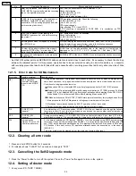
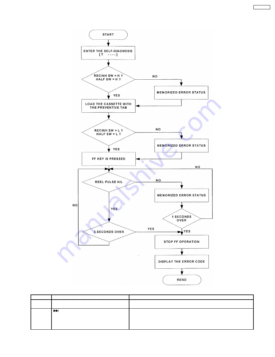
 5. After the tape stops, the Error codes will be displayed by toggling the STOP

n

key. For more detail explanation, refer to the

(Figure 12-2).

Figure 12-2

No.

Operation Procedures

Micon operation & processing

1

C-mecha Abnormal Detection shall be
executed for DECK 1 only.

Check that all DECK mechanism leaf SW are in OFF state.

2

[

] key is pressed, after loading in a

NORMAL type cassette with the recording tab
on the left side removed.

FF shall be executed for 2 sec, afterwhich STOP.
Check the following.
{ F.REC INH SW } is OFF
{ HALF SW } is ON
Reel pulse toggles between H & L.

31

SA-PM21PC

Summary of Contents for SA-PM21PC

Page 1: ...ity S N 20 dB at 1000 kHz 500 µV m 2005 Matsushita Electric Industrial Co Ltd All rights reserved Unauthorized copying and distribution is a violation of law SA PM21PC Colour S Silver Type n Cassette Deck Section Track system 4 track 2 channel Heads Record playback Solid permalloy head Erasure AC erase head Motor DC servo motor Recording system AC bias 100 kHz Erase system AC erase 100 kHz Tape sp...

Page 2: ...cedures for Replacement Traverse Gear A and Traverse Gear B CD Mechanism Unit 23 Dimensions W x H x D 165 x 228 x 315 6 mm 6 1 2 x 9 x 12 7 16 Mass 3 6 kg 7 9 Ibs Power consumption in standby mode 0 5 W Notes 1 Specifications are subject to change without notices Mass and dimensions are approximate 2 Total harmonic distortion is measured by the digital spectrum analyzer n System SC PM21PC S Music ...

Page 3: ...rmer P C B and Tape Eject P C B 69 20 Wiring Connection Diagram 70 21 Illustration of IC 痴 Transistors and Diodes 72 22 Terminal Function of ICエs 73 22 1 IC702 MN6627953HB Servo processor Digital signal processor Digital filter D A converter 73 22 2 IC703 BA5948FPE2 IC 4CH DRIVE 74 22 3 IC803 MN101C49GHA MICRO PROCESSOR 75 23 Troubleshooting Flowchart CD Section Circuit 76 24 Parts Location and Re...

Page 4: ...tance value between the jumpered AC plug and each exposed metallic cabinet part on the equipment such as screwheads connectors control shafts etc When the exposed metallic part has a return path to the chassis the reading should be between 1MΩ and 5 2Ω When the exposed metal does not have a return path to the chassis the reading must be Fig 1 1 1 2 LEAKAGE CURRENT HOT CHECK See Figure 1 1 Plug the...

Page 5: ...1 1 3 Caution for fuse replacement 5 SA PM21PC ...

Page 6: ... the amplifier are used If this occurs follow the procedure outlines below 1 Turn off the power 2 Determine the cause of the problem and correct it 3 Turn on the power once again after one minute Note When the protection circuitry functions the unit will not operate unless the power is first turned off and then on again 4 Handling the Lead free Solder 4 1 About lead free solder PbF Distinction of ...

Page 7: ...riable resistor on the pickup lens 4 Do not disassemble the optical pick up unit 5 If the optical pick up is replaced use the manufacturer s specified replacement pick up only 6 Use of control or adjustments or performance of procedures other than those specified herein may result in hazardous radiation exposure CAUTION THIS PRODUCT UTILIZES A LASER USE OF CONTROLS OR ADJUSTMENTS OR PERFORMANCE OF...

Page 8: ...variable resistor laser power adjustment It has already been adjusted Fig 6 1 l Grounding for electrostatic breakdown prevention 1 Human body grounding Fig 6 2 Use the anti static wrist strap to discharge the static electricity from your body 2 Work table grounding Fig 6 2 Put a conductive material sheet or steel sheet on the area where the traverse deck optical pickup is placed and ground the she...

Page 9: ...Remote control AC cord FM indoor antenna AM loop antenna 7 Accessories Note Refer to Packing Materials Accessories Section 24 5 for part number 9 SA PM21PC ...

Page 10: ...8 Operation Procedures 10 SA PM21PC ...

Page 11: ...9 Information on CD MP3 11 SA PM21PC ...

Page 12: ...cks or replacement reverse the respective procedures Special reassembly procedures are described only when required 3 Select items from the following index when checks or replacement are required Warning This product uses a laser diode Refer to Precaution of Laser Diode 10 1 Disassembly flow chart The following chart is the procedure for disassembling the casing and inside parts for internal inspe...

Page 13: ...areful of the catches 10 3 Disassembly of Top Cabinet Unit Follow the Step 1 Step 6 of Item 10 2 Step 1 Remove 1 screw Step 2 Release catches at both ends Step 3 Lift up the top cabinet unit push backward as arrow shown and flip top cabinet unit sideway Step 4 Detach the connectors CN504A and FFC CN804 10 4 Disassembly of Deck Mechanism and Tape Eject P C B Follow the Step 1 Step 6 of Item 10 2 Fo...

Page 14: ...he deck mechanism unit 10 5 Disassembly of Headphone P C B Follow the Step 1 Step 6 of Item 10 2 Follow the Step 1 Step 4 of Item 10 3 Step 1 Remove 1 screw Step 2 Release the clutch 10 6 Disassembly of Front Panel Assembly Follow the Step 1 Step 6 of Item 10 2 Follow the Step 1 Step 4 of Item 10 3 Step 1 Detach the connector CN900B 14 SA PM21PC ...

Page 15: ... the Step 1 Step 4 of Item 10 6 Step 1 Remove 10 screws Step 2 Remove the Volume Knob 10 8 Disassembly of Rear Cabinet Follow the Step 1 Step 6 of Item 10 2 Follow the Step 1 Step 4 of Item 10 3 Step 1 Remove 6 screws Step 2 Remove the rear cabinet as arrow shown 10 9 Disassembly of Tuner Pack Follow the Step 1 Step 6 of Item 10 2 Follow the Step 1 Step 4 of Item 10 3 Follow the Step 1 Step 2 of I...

Page 16: ...1 Step 4 of Item 10 6 Follow the Step 1 Step 2 of Item 10 8 Step 1 Detach the FFC CN801 Step 2 Detach the connector CN803A CN808A Step 3 Detach the connector CP800 Step 4 Remove the Main P C B as arrow shown 10 11 Disassembly of Power P C B Follow the Step 1 Step 6 of Item 10 2 Follow the Step 1 Step 4 of Item 10 3 Follow the Step 1 Step 2 of Item 10 8 Step 1 Detach the connector CN505B 16 SA PM21...

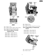
Page 17: ... 2 of Item 10 8 Follow the Step 1 Step 2 of Item 10 10 Follow the Step 2 Step 4 of Item 10 11 Step 1 Remove 1 screw Step 2 Release the clutch Step 3 Remove the Speaker Terminal P C B as arrow shown 10 13 Disassembly of Transformer P C B Follow the Step 1 Step 6 of Item 10 2 Follow the Step 1 Step 4 of Item 10 3 Follow the Step 1 Step 2 of Item 10 8 Follow the Step 1 Step 4 of Item 10 11 Step 1 Det...

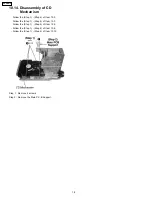
Page 18: ...p 1 Step 6 of Item 10 2 Follow the Step 1 Step 4 of Item 10 3 Follow the Step 1 Step 4 of Item 10 6 Follow the Step 1 Step 2 of Item 10 8 Follow the Step 1 Step 4 of Item 10 10 Step 1 Remove 4 screws Step 2 Remove the Main P C B Support 18 SA PM21PC ...

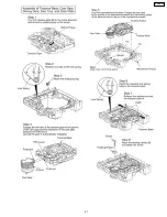
Page 19: ...der the terminals of Power Amp IC IC300 IC500 and replace the component Step 3 Unsolder the terminals of Transistor Q503 and replace the component 10 16 Procedures of Replacing Traverse Base Unit Driving Gear and Cam Gear CD Mechanism Unit 10 16 1 Disassembly of the Disc Tray Follow the Step 1 Step 6 of Item 10 2 Follow the Step 1 Step 4 of Item 10 3 Follow the Step 1 Step 4 of Item 10 6 Follow th...

Page 20: ...20 SA PM21PC ...

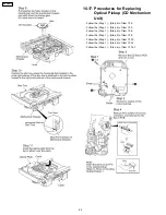
Page 21: ...21 SA PM21PC ...

Page 22: ...e Step 1 Step 6 of Item 10 2 Follow the Step 1 Step 4 of Item 10 3 Follow the Step 1 Step 4 of Item 10 6 Follow the Step 1 Step 2 of Item 10 8 Follow the Step 1 Step 4 of Item 10 10 Follow the Step 1 Step 2 of Item 10 14 Follow the Step 1 Step 4 of Item 10 16 1 22 SA PM21PC ...

Page 23: ...it Follow the Step 1 Step 6 of Item 10 2 Follow the Step 1 Step 4 of Item 10 3 Follow the Step 1 Step 4 of Item 10 6 Follow the Step 1 Step 2 of Item 10 8 Follow the Step 1 Step 4 of Item 10 10 Follow the Step 1 Step 2 of Item 10 14 Follow the Step 1 Step 2 of Item 10 16 1 23 SA PM21PC ...

Page 24: ...1 Step 6 of Item 10 2 Follow the Step 1 Step 4 of Item 10 3 Follow the Step 1 Step 4 of Item 10 4 10 20 Procedure for Replacing Pinch Roller and Head Block Deck Mechanism Unit Follow the Step 1 Step 6 of Item 10 2 Follow the Step 1 Step 4 of Item 10 3 24 SA PM21PC ...

Page 25: ...e for Replacing Motor Capstan Belt A Capstan Belt B and Winding Belt Deck Mechanism Unit Follow the Step 1 Step 6 of Item 10 2 Follow the Step 1 Step 4 of Item 10 3 Follow the Step 1 Step 4 of Item 10 4 Follow the Step 1 Step 4 of Item 10 20 25 SA PM21PC ...

Page 26: ...26 SA PM21PC ...

Page 27: ...Item 10 2 10 22 Procedure for Replacing Parts on Deck Mechanism PCB Follow the Step 1 Step 6 of Item 10 2 Follow the Step 1 Step 4 of Item 10 3 Follow the Step 1 Step 4 of Item 10 4 10 23 Handling of cassette tape jam 27 SA PM21PC ...

Page 28: ...28 SA PM21PC ...

Page 29: ...f Rear Cabinet 8 Disassembly of Tuner Pack 9 Disassembly of Main P C B 10 Disassembly of Power P C B 11 Disassembly of Speaker Terminal P C B 12 Disassembly of Transformer P C B 13 Disassembly of CD Mechanism Service tools Extension cable Main P C B and Speaker Terminal P C B RFKPM21 11 Service Positions 11 1 Checking procedure Note For the disassembling procedure see the section 10 11 2 Checking ...

Page 30: ...umber can be cleared only at the start up of micro p after reset If repeating self diagnosis add the newly detected errors only without deleting errors which have been detected before 12 1 4 Self diagnosis mode Deck Mechanism Activate the Self Diagnosis mode for the Deck and the following Self Diagnosis will be conducted Error Code Description H01 If MODE SW abnormal is detected during normal oper...

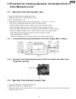
Page 31: ...con operation processing 1 C mecha Abnormal Detection shall be executed for DECK 1 only Check that all DECK mechanism leaf SW are in OFF state 2 key is pressed after loading in a NORMAL type cassette with the recording tab on the left side removed FF shall be executed for 2 sec afterwhich STOP Check the following F REC INH SW is OFF HALF SW is ON Reel pulse toggles between H L 31 SA PM21PC ...

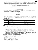
Page 32: ...rmal operation if mechanism error process is executed once by mode switch against the same deck operation it is judged as mechanism abnormality and this is memorized as an error Conditions for judging mechanism error Mode switch ON is not detected 800 ms after plunger activation for PLAY REC process Mode switch ON is not detected 800 ms after plunger activation for FF REW process Or Mode switch OF...

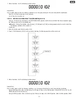
Page 33: ... CD Unit Combination Test 10 1 2 4 EEPROM Checksum Check DOCTOR MODE C2DF 4 7 5 Cold Start Setting SLEEP Note If entering Doctor Mode by numeric buttons PRESET EQ and SURROUND will be set to OFF In case of error all the segments of FL will blink 0 5 sec ON OFF and Doctor Mode shall be retained The operation key used for the test follows closely with the test items as far as possible to facilitate ...

Page 34: ...operation stop the aging test at CLOSE condition During CLOSE operation after a certain timing the CD does not close in the CLOSE position After CLOSE operation REST SW was not turned off in 4s Do the OPEN operation stop the aging test at OPEN condition 12 4 3 CD Unit Traverse Test Reliability test 2 Purpose Access Inner Outer Disc aging test To test CD Unit traverse reliability The following oper...

Page 35: ...0 followed by 1 3 are being pressed using the remote control key the following operation will be carried out Procedures 1 Enter into doctor mode Refer to section 12 4 2 Press 10 followed by 1 3 on the remote control key the following operation will be carried out 3 After a few times the FL will display as shown below Special Note Due to certain reason when the following conditions occur the aging ...

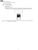
Page 36: ...ss has not yet complete Out of Focus for more than 2s 12 4 5 Cold start setting Note In the case that you unplug from AC outlet after this mode was set then plug to AC again a cold start shall begin And is displayed in the FL for 2 seconds 36 SA PM21PC ...

Page 37: ...al timing at STOP mode ON approx 200msec e REV REW Supply the plunger power in a flash at REV PLAY mode ON approx 50msec f STOP Supply the plunger power in a flash at FF mode ON approx 50msec Repeat the operation FWD PLAY Note Other operation may start if a timing of supplying the plunger power is missed 13 1 1 Connection Status between Mechanism and Power Supply Motor Plunger 13 1 2 Operative Par...

Page 38: ...Fig 7 38 SA PM21PC ...

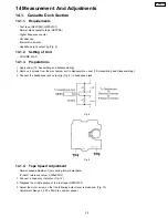
Page 39: ...bling 2 Remove 4 screws from the mechanism unit to disassemble under 10 Assembling and Disassembling 3 Connect the headphone jack output jig Fig 8 to headphone jack Fig 8 Fig 9 14 1 4 Tape Speed Adjustment Normal speed adjustment only during forward playback Product reference value 3 000 90Hz 1 Connect a frequency indicator Fig 12 2 Playback the middle portion of the test tape QZZCWAT 3 Adjust the...

Page 40: ...mode Repeat pressing the buttons till the recording pause mode is activated 5 Check that the output level is within the standard range Standard Range 16 3mV Fig 12 14 1 6 Bias Frequency Check 1 Connect a digital frequency counter Fig 13 2 Set the function to TAPE position 3 Insert a normal blank cassette tape QZZCRA and press REC mode on main unit 4 Check that the output frequency is within the st...

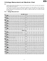
Page 41: ... 0 0 0 7 5 4 3 3 5 3 5 3 5 3 1 3 9 3 6 3 5 7 6 0 STANDBY 0 0 0 0 0 0 0 0 0 0 0 0 0 0 0 0 0 0 0 0 Ref No MODE 21 22 23 24 25 26 27 28 CD PLAY 7 6 0 0 0 7 6 1 7 1 7 1 7 STANDBY 0 0 0 0 0 0 0 0 Ref No MODE 1 2 3 4 5 6 7 8 CD PLAY 4 5 4 4 4 4 0 4 4 4 4 4 5 8 8 STANDBY 0 0 0 0 0 0 0 0 Ref No MODE 1 2 3 4 5 6 7 8 9 10 11 12 13 14 15 16 17 18 19 20 CD PLAY 4 4 4 4 4 4 4 4 4 4 4 4 4 4 4 4 4 4 4 4 4 4 0 0 ...

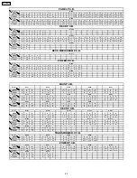
Page 42: ...00 IC 971 DECK MECHANISM P C B IC 1001 Ref No MODE E C B E C B E C B E C B E C B CD PLAY 0 0 0 0 0 0 4 5 8 3 5 2 3 3 8 2 3 9 0 0 0 STANDBY 0 0 0 0 0 0 0 0 0 0 0 0 0 0 0 Ref No MODE E C B E C B 1 2 3 E C B E C B CD PLAY 0 0 0 4 5 8 3 5 2 3 3 8 2 3 9 0 4 8 0 0 1 0 1 2 STANDBY 0 0 0 0 0 0 0 0 0 0 0 2 0 0 0 3 0 Ref No MODE E C B E C B E C B E C B CD PLAY 0 0 4 6 0 4 7 0 0 9 7 0 0 9 7 0 STANDBY 0 0 0 0...

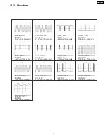
Page 43: ...N801 PIN 7 CD PLAY 3 48Vp p 5msec div CN801 PIN 8 CD PLAY 3 12Vp p 5msec div CN803B PIN 5 CD PLAY 5 76Vp p 25msec div CN900B PIN 3 CD PLAY 4 28Vp p 25msec div CN900B PIN 4 CD PLAY 4 32Vp p 25msec div CN901B PIN 9 CD PLAY 5 64Vp p 25msec div CN901B PIN 11 CD PLAY 5 36Vp p 25msec div CN901B PIN 12 CD PLAY 5 80Vp p 25msec div CN801 PIN 4 CD PLAY 3 64Vp p 5msec div 43 SA PM21PC ...

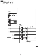
Page 44: ...H DRIVE IN4 27 TRP IN3 28 FOP IN2 1 TRVP IN1 3 SPOUT PC2 2 VREF 26 D4 17 D4 18 D3 15 D3 16 D2 14 D2 13 M701 TRAVERSE MOTOR D1 12 D1 11 M702 SPINDLE MOTOR B E E E E E F E F D C A B D C FOCUS COIL TRACKING COIL T OPTICAL PICKUP PHOTO DETECTOR SEMICONDUCTOR LASER F F T Q701 LASER POWER DRIVE PC1 4 SPPOL B M M C B E A D F LPD LD 44 SA PM21PC ...

Page 45: ...TER D A CONVERTER A 6 11 7 5 SPOUT SPPOL TRVP TRP FOP LD PD BLK CK NRST STAT MLD MDATA MCLK A C B D F E 63 64 65 66 54 OUTL OUTR SPOUT SPPOL PC TRVP TRP FOP LD PD 50 RCH CD SIGNAL BLK CK NRST STAT MLD MDATA MCLK A C B D F E 67 13 X701 70 71 X2 X1 35 34 33 32 31 30 28 29 68 45 SA PM21PC ...

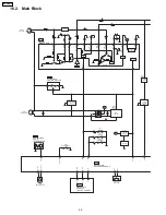
Page 46: ... SW 9 ALC SWITCH LOGIC NOR CRO SW 13 VCC 12 RF REC L OUT R 15 8 ALC 14 10 20 3 18 19 4 TPS GAIN ADJ 17 REC LIN R 16 7 FILTER 21 2 REC AMP L RIPPLE REJECTION MUTE Q1309 Q1310 Q1312 L1301 D1301 Q1317 BEAT PROOF LEVEL SWITCH DECK 2 ERASE HEAD DECK 2 R P HEAD LCH S971 MODE S972 HALF S974 RECIN_H Q1304 Q1101 Q1201 MUTING SWITCH SWITCH DECK MUTING CONT BIAS SWITCH 78 DMT 75 PHOTO 74 TAPE_EJECT S1000 TAP...

Page 47: ...R SWITCH SWITCH MOTOR SUPPLY 71 PL_H PLUNGER SWITCH Q808 Q807 66 TUN_STEREO 65 TUN_TUNED 47 TUN_CL 45 TUN_SDA TUNER PACK X801 OSC2 12 OSC1 13 X802 XI 15 XO 16 RMT 26 RESET SWITCH Q804 NRST 33 17 16 OUT1 2 14 S1 13 SC 4 3 SEL1OUT 2 1 2 VIN1 2 9 10 C1IN 2 7 8 B1IN 2 Q221 Q222 Q421 Q422 AMPLIFIER 57 ASP_DATA 56 ASP_CLK 5 6 A1IN 2 LOW PASS FILTER HI PASS FILTER Q290 Q490 Q280 Q480 B 47 SA PM21PC ...

Page 48: ...FL_DATA 44 FL_CLK 10 DATA 9 CLK FL900 FL DISPLAY SEG1 SEG20 FROM TRANSFORMER 21 CD_MDATA 22 STAT 23 CD_MCLK 28 CD_OPENSW 29 REST_SW 30 BLKCK 35 CD RST 36 CD_MLD 98 CLOSE_L 99 OPEN_H D804 D803 Q801 SWITCH Q802 SWITCH MDATA STAT MCLK BLKCK NRST MLD LOADING LD_SW CLDCK S701 REST SW 33 40 S701 CD_OPEN SW GRID1 GRID10 12 14 16 20 33 40 C 48 SA PM21PC ...

Page 49: ...EGULATOR SYS6V Q600 PCONT SWITCH Q602 SWITCH D608 D501 D502 D504 D505 TO FL DISPLAY Q603 SWITCH D609 Q503 STABALIZER Q501 SWITCH Q504 SWITCH Q530 Q506 REGULATOR Q505 D513 25 PCONT_1 Z600 Q500 CURRENT LIMITTING 9 MUTE 12 2 LOW L LOW R 5 STBY 8 6 IN_L IN_R 49 D380 10 4 LOW L LOW R PCONT_2 D751 REGULATOR REGULATOR 15 2 OUT GND 9 B B B B B B B B MAIN SIGNAL LINE FM AM SIGNAL LINE CD SIGNAL LINE TAPE R...

Page 50: ...n the basis of chassis Accordingly there may arise some error in voltage values and waveforms depending upon the internal impedance of the tester or the measuring unit Importance safety notice Components identified by mark have special characteristics important for safety Furthermore special parts which have purposes of fire retardant resistors high quality sound capacitors low noise resistors etc...

Page 51: ...IN3 D2 D2 D1 D1 PVCC1 PGND1 NC GND NC NC NC PC1 IN1 PC2 IN2 IC703 BA5948FPE2 IC 4CH DRIVE CN701 28 27 26 3 2 1 25 4 24 5 23 6 22 7 19 10 18 11 17 12 16 13 15 14 20 21 9 8 VCC F E LD LD GND GND A GND B VREF LPD GND T T F F C714 6 3V100 R739 1K 15 14 13 12 11 10 2 4 6 8 9 7 5 3 1 16 C1 0 47 C9 0 22 TRACKING COIL FOCUS COIL VCC F E LD LD GND GND A GND B VREF LPD GND T T F F HUL7213 E Vref A NC LPD GN...

Page 52: ...D RFOUT CEA LD C RFENV RESERVE AVDD2 NTEST CAGC PLFF0 ARFOUT AVSS2 ARFIN DSLF IREF PLLF AVSS1 NC OUTR IOVDD1 REGON IOMODE DVSS2 AVDD1 OUTL DVDD2 STAT TX 50 C707 0 022 C705 0 1 C706 0 1 R706 1K R704 1K C747 390P R744 47K C742 0 022 C710 470P R702 4 7K R705 39K C749 3900P C760 0 1 51 C716 680P R711 82K C744 0 015 C717 0 1 C741 1000P C718 0 082 R712 820 C704 0 1 C703 6 3V100 R721 100 C762 0 1 R764 1K...

Page 53: ...HOTO REC_RCH TAPE_EJECT REC_LCH VREF PB_RCH AN7 PB_LCH AN6 MOTOR_10V PL_L MOTOR_L 9VGND RECH 9V D9V DMT PHOTO REC_RIN TAPE_EJECT REC_LIN VREF AGND VREF PB_ROUT AN7 PB_LOUT AN6 MOTOR_10V PL_L MOTOR_GND MOTOR_L PORTSEL CL SDA TUNED LCH SETERO RCH DET TUNER_9V TUNER_GND CN901B 12 11 10 2 4 6 8 9 7 5 3 1 VREF D5V KEY2 KEY1 VREF VOL_JOG2 VOL_JOG1 RMT FL_CLK FL_RST FL_DAT FL_CS D5V KEY2 KEY1 VREF VOL_JO...

Page 54: ...ASP_CLK Q751 Q421 VIN1 VIN2 SEL2OUT SEL1OUT A1IN A2IN B1IN B2IN C1IN C2IN FILTER GND IC800 C1BB00000757 ASP IC MAIN SIGNAL LINE TAPE PLAYBACK SIGNAL LINE TAPE RECORD SIGNAL LINE CD SIGNAL LINE FM AM SIGNAL LINE B SIGNAL LINE 1 2 3 4 6 7 8 5 R800 4 7 IC700 C0ABBB000297 OP AMP Q751 B1GBCFJJ0044 SWITCH Q803 Q803 B1GBCFJJ0044 MUTING SWITCH C296 50V0 22 Q490 Q290 Q280 Q480 C481 2200P C482 1000P C282 10...

Page 55: ...8 7 9 11 13 15 1 2 1 2 Q801 2 4 6 8 9 7 5 3 1 CN803B VREF D5V CD_DGND 9V GND HALT PCONT_1 SYS 6V CD_7 5V PGND R880 4 7K C851 0 01 R877 22K R878 22K R879 100K E_CS E_CLK E_DATA VREF C852 100P MAIN SIGNAL LINE CD SIGNAL LINE B SIGNAL LINE IC804 C3EBCG000031 EEPROM NOT SUPPLIED R805 10K CD_RST LOADING S780 CD OPEN SW HI_LEFT AGND HI_RIGHT TUNER_9V TNR_GND LOW_L AGND LOW_R A 9V MUTEB MOTOR_GND MOTOR_1...

Page 56: ...TEREO TUNED TAPE_EJECT A 9V KEY1 KEY2 AN6 REC_H DMT VOL_JOG1 VOL_JOG2 X802 FL_DATA FL_CS FL_RST SDA FL_CLK CL VREF VREF VREF CD_MLD CD_RST VDD BLKCK REST_SW HALT RMT CD_OPEN_SW VREF DEMO SETTING PCONT2 NC TUN_CL NC TUN_SDA FL_CLK NC FL_DATA FL_CS FL_RST NC NC NC CD_MLD CD_RESET NC MICOM RST NC NC BLKCK REST_SW HALT RMIN CD_OPS PHOTO_1 TAPE_EJ NC NC PL_H MOTOR_H NC NC NC TU_ST TU_TUNED NC E_CS E_CL...

Page 57: ...L_CS WH900A JW900A VP SEG02 SEG01 GRID10 SEG19 SEG20 YP SEG03 SEG04 SEG05 SEG06 SEG07 SEG08 SEG09 SEG10 SEG11 SEG12 SEG13 SEG14 SEG15 SEG16 SEG17 SEG18 RST CS SCK DATA VCC XOUT XIN IC900 C0HBB0000044 FL DRIVER IC 1 2 3 4 5 6 7 8 9 10 11 12 13 14 15 16 17 18 19 20 21 22 23 24 25 26 27 28 29 30 31 32 33 34 35 36 37 38 39 40 41 42 43 44 2 4 3 1 FL900 A2BB00000138 FL DISPLAY D5V GRID9 GRID8 GRID7 GRID...

Page 58: ...K R1305 10K C1305 16V33 C1308 16V22 C1102 470P C1101 50V1 R1101 27 C1104 0 027 C1103 16V100 C1121 0 001 R1102 1 5K C1107 1500P C1106 50V2 2 C1302 0 033 R1104 10K C1122 0 01 R1103 18K C1105 470P R1302 330 C1303 0 033 C1123 270P C1108 16V10 R1303 4 7M C1304 50V4 7 C1307 10V220 R1308 22 R1307 22 RECH1 C1204 16V 0 027 1 2 4 3 5 VCC H OFF IC1000 C1AA00000612 ANALOG SWITCH IC L1301 7L1A62N 6 5 4 4 2 1 3...

Page 59: ...H0002 MOTOR SUPPLY SWITCH R1341 470 R1374 470 Q1316 Q1314 R1342 47K R1343 3 3K R1345 1K Q1315 R1344 27K C1326 16V10 Q1315 KTA12710YTA SWITCH 1 2 1 2 RECH1 PHOTO RECH AN7 AN6 MODE HALF PL PL_GND PHOTO_T RECINH_F VREF VREF CR02 Q1101 Q1201 B1ABGC000005 MUTING SWITCH Q1201 CN1303 VREF 9VGND RECH 9V DMT PHOTO REC_RIN TAPE_EJECT REC_LIN VREF AGND VREF PB_ROUT AN7 PB_LOUT AN6 MOTOR_9V PL_L MOTOR_GND MOT...

Page 60: ...V1 FP552 2A K5G202A00025 R576 2 2K R577 2 2K C572 16V470 R578 120 R579 120 R568 120 R569 120 R566 2 2K R567 2 2K C552 16V470 FP352 5A K5G502A00039 C586 16V10 R586 47K C368 16V22 R381 47K C551 50V1 C581 16V470 R581 22K R580 5 6K D580 B0AACK000004 C571 50V1 C570 470P R571 1K R570 3 3K C550 470P R551 1K R550 3 3K 1 2 3 4 5 6 8 7 LOW L LOW L LOW R LOW R HI_R GND1 HI R GND HI_L GND1 HI L GND LOW R LOW ...

Page 61: ... 10 11 15 16 14 12 2 3 5 2 1 3 4 R430 100K C430 0 01 L600 G0B371HA0005 PCONT_2 MOTOR_10V MOTOR_GND MUTEB A 9V LOW_R AGND LOW_L TUNER_GND A9V HI_RIGHT AGND HI_LEFT PCONT_2 MOTOR_10V MOTOR_GND MUTEB A 9V LOW_R AGND LOW_L TUNER_GND A9V HI_RIGHT AGND HI_LEFT Lch Rch D606 D611 B0EAKM000122 JK501 R609 3 3M TO PANEL CIRCUIT WH900A JW900A ON SCHEMATIC DIAGRAM 7 TO POWER CIRCUIT WH505A JW505A ON SCHEMATIC ...

Page 62: ... J725 R753 R764 R720 R714 C722 C721 C745 J716 C743 J723 J703 C733 J715 J705 C755 C705 C746 J702 J706 J707 J708 J709 J717 J718 C706 J742 J741 J712 J739 J733 J734 C740 TP2 TP18 TP17 TP19 TP16 TP13 TP14 TP11 TP12 TP53 TP24 TP73 TP74 TP75 TP78 TP70 TP69 TP64 TP63 TP62 TP1 TP8 TP9 TP10 TP37 TP39 TP55 TP35 TP61 TP71 TP68 TP72 TP33 TP49 TP28 TP29 TP48 TP94 TP84 TP95 TP93 TP89 TP60 TP82 TP83 TP34 TP36 TP2...

Page 63: ... WA11 D751 R752 D750 R751 R750 R222 R C423 IC R890 R891 WA15 CN901B CN804 C817 R884 R883 CN801 L812 CN803B WA16 WA17 R815 W400 W700 W250 W251 W401 W200 W402 CN805A TO TUN W403 W404 R869 W201 W202 W203 W405 W406 C818 CN504A C850 WA08 X802 R840 R804 C750 IC803 W208 W209 W210 W431 W213 W214 W215 W408 W409 W410 W411 W412 W413 W414 W415 W416 W417 W418 W730 W419 W218 W420 W760 W731 W732 W421 W701 W702 W...

Page 64: ...TUNER PACK Z401 ENG06810QF W403 W404 W201 W202 W405 C224 W406 W205 C410 C210 C481 C482 R482 R485 Q480 R483 R484 R494 C493 C492 R492 R495 R491 C281 R285 Q280 C282 R282 R284 R283 C413 C213 Q290 R294 C293 C292 R292 R291 R295 W407 R467 R466 R267 R266 WA81 WA82 C496 C283 C296 C483 W206 C880 C212 C750 C751 R753 W207 Q490 CN808B W213 W214 W216 W805 W704 W256 W705 W706 W768 W769 W770 W707 W708 W709 W425 W...

Page 65: ... R230 R430 W360 W370 W350 W351 CN501B JK501 JK502 E301 CN808A CN803A CN503A CN508A C371 W310 W311 HEADPHONE CN805B CN806 TO Z401 TUNER PACK ENG06810QF HIGH CH SPEAKER LOW CH SPEAKER C102 C101 4 1 2 3 4 5 6 7 8 9 1 2 3 4 5 6 7 8 9 10 11 12 13 1 2 3 4 5 6 7 8 9 1 2 3 4 5 6 7 8 9 10 11 12 13 1 2 3 4 5 6 7 8 1 L 3 R 2 GND L 4 GND R 1 L 3 R 2 L 4 R 3 2 1 1 G 3 R 5 G 4 G 2 L 6 SW 7 G 1 2 3 4 5 6 7 8 9 1...

Page 66: ... W940 W900 W901 W941 W920 R920 L901 C903 C911 C910 C909 W942 W962 W921 W922 C904 W960 W945 W946 W902 L905 W961 FL900 W943 D906 VOLUME SENSOR R905 R906 R914 R913 R904 R902 R901 R900 R912 R911 R909 R910 R903 C900 C901 R916 R924 R908 R925 R915 C908 R921 R919 C914 C906 R917 C905 C907 R918 C912 R923 R922 D900 C913 1 1 1 1 3 5 6 7 8 9 10 11 12 13 14 15 16 17 18 19 20 21 22 23 24 25 26 27 28 29 30 31 32 ...

Page 67: ...C1222 C1371 R1341 C1204 Q1303 R1209 R1109 Q1314 R1206 Q1201 Q1304 R1314 R1305 R1205 R1105 R1106 R1313 R1207 R1107 Q1302 Q1101 R1344 R1343 R1374 R1345 R1342 R1328 R1331 Q1312 R1332 R1338 R1334 D1301 R1329 R1327 C1315 C1312 C1314 C1316 C1317 R1335 Q1317 R1337 R1302 C1107 R1110 C1302 C1303 C1105 R1103 C1102 R1210 R1104 R1371 R1203 R1101 C1104 R1303 R1304 C1207 C1205 R1204 R1201 R1102 C1121 R1202 C122...

Page 68: ... R586 C586 D582 FP552 2A D580 C570 C550 C368 D380 R351 C350 R352 R370 R371 D513 FP352 5A CN508B CN503B CN501A C372 C373 C351 C352 W500 W520 W521 W522 W540 W552 W553 W554 W560 W563 W562 W561 W571 W570 W572 W577 W576 W581 W580 W585 W590 C374 W505 Q530 C507 C530 D512 C540 R530 Q506 R517 C514 D506 C541 Q505 R518 C515 D507 C542 W545 Q503 W506 R579 R578 R569 R568 R577 R576 R567 R566 C522 C521 C523 C524 ...

Page 69: ...1 TRANSFORMER W620 W615 Z600 D605 D603 D606 D604 C601 W600 C603 D611 R601 CN505B R604 R600 Q600 W617 D600 R603 R605 C605 Q601 C604 D607 Q602 D608 R607 R606 D609 D602 C612 R608 R611 D610 C610 C611 Q603 CN900B FC601 FC600 JK600 L600 C609 W601 W602 W603 W604 W610 W605 W301 AC IN F1 125V 1 6A 120V 60Hz R609 1 2 2 3 4 1 2 3 4 5 6 7 8 E C B E C B E C B E C B 1 3 4 2 3 5 6 16 15 14 12 11 10 5 1 4 3 2 4 3...

Page 70: ... 4 9 1 SENSOR VOLUME CN702 CN701 CP1902 JW1903 CP1301 CN1303 CS971 SOLENOID JW308A 1 2 3 4 5 1 2 1 2 1 2 17 1 16 2 1 9 19 1 18 2 11 1 12 2 PANEL P C B CD SERVO P C B TRANSFORMER P C B DECK P C B TAPE EJECT P C B DECK MECHANISM P C B OPTICAL PICKUP PL PL PbF PbF PbF PbF PbF PbF SOLDER SIDE SOLDER SIDE SOLDER SIDE SOLDER SIDE SOLDER SIDE SOLDER SIDE WH900A JW900A 70 SA PM21PC ...

Page 71: ...9 1 13 1 8 1 HEADPHONE CN805B CN806 4 1 4 1 1 10 1 10 11 1 12 2 1 8 MAIN P C B HEADPHONE P C B TUNER EXTENT P C B SPEAKER TERMINAL P C B POWER P C B CN901B CN804 CN801 CN803B CN805A CN504A CN808B CP800 WH505A JW505A CN508B CN503B CN501A PbF SOLDER SIDE PbF PbF PbF SOLDER SIDE SOLDER SIDE SOLDER SIDE SOLDER SIDE PbF J 2 1 HIGH CH SPEAKER LOW CH SPEAKER Z401 71 SA PM21PC ...

Page 72: ... KRC101STA KRC104STA 2SD0592ARA 2SD09650RA KTA12710YTA KTC32030YTA B C E A Ca Anode Cathode B0ACCK000005 2SC3940ARA B0ACCE000003 B0BC6R700006 A Ca Anode Cathode MAZ80560ML A Ca Anode Cathode B0BA5R600016 B0BA9R600002 B0BA8R200005 B0EAKM000117 B0EAMM000038 B0EAKM000122 B1GBCFJJ0044 B1ABCE000016 B1ADCF000001 1 3 4 5 2 B1BCCG000002 2SB0621AHA B0AACK000004 MA2C16500E B0BA6R800007 B0BA02600017 B3AAA000...

Page 73: ...nal 37 RFVDD RF Amp power supply 38 RESERVE AVSS2 Pin No Mark I O Function 39 RFOUT O RF Amp output 40 RFIN I AGC input 41 CAGC I O AGC control terminal 42 ARFOUT O AGC output Audio RF 43 AVSS2 Analog circuit GND 2 44 ARFIN I RF signal input 45 DSLF O DSL loop filter 46 IREF I I current Reference input 47 PLLF O PLL loop filter 48 PLLF0 O PLL loop filter 49 AVDD2 Analog circuit power supply 2 50 O...

Page 74: ...Motor Driver 2 reverse action output 14 D2 O Motor Driver 2 forward action output Pin No Mark I O Function 15 D3 O Motor Driver 3 reverse action output 16 D3 O Motor Driver 3 forward action output 17 D4 O Motor Driver 4 reverse action output 18 D4 O Motor Driver 4 forward action output 19 PVCC2 Power Supply 2 for Driver 20 PGND2 Ground Connection 2 for Driver 21 N C No Connection 22 N C No Connect...

Page 75: ... For Tuner 48 N C No Connection 49 PCONT2 I O Power Control Output2 PWR AMP active H 50 DEMO SETTING I O Demo Mode Setting H OFF L ON 51 N C No Connection 52 HP_SW I O Headphone Detect SW Input 53 MUTE A I O Audio Mute O P L Mute On 54 N C No Connection 55 N C No Connection 56 ASP_CLK I O ASP CLK O P 57 ASP_DAT I O ASP Data O P 58 N C No Connection 59 N C No Connection 60 N C No Connection 61 EDAT...

Page 76: ...23 Troubleshooting Flowchart CD Section Circuit 76 SA PM21PC ...

Page 77: ...77 SA PM21PC ...

Page 78: ...ads µF unless specified otherwise P Pico farads pF F Farads Resistance values are in ohms unless specified otherwise 1K 1 000 OHM The marking RTL indicates that the Retention Time is limited for this items After the discontinuation of this assembly in production the item will continue to be available for a specific period of time The retention period of a availability is dependent on the type of a...

Page 79: ...24 1 Deck Mechanism 24 1 1 Deck Mechanism Parts Location RAA4402 S 79 SA PM21PC ...

Page 80: ... LEVER M 118 RML0372 WINDING LEVER M 119 RML0374 EJECT LEVER M 120 RMM0131 BRAKE ROD M 121 RMM0133 EJECT ROD M 122 RMQ0519 REEL HUB M 123 RMS0398 1 MOVING CORE M 124 RXQ0470 PLUNGER M 125 RMC0061 PACK SPRING M 126 RXF0061 FLYWHEEL F ASS Y M 128 RXG0040 FF RELAY GEAR ASS Y M 129 RMK0283A J SUB CHASSIS M 130 RXL0124 PINCH ROLLER F ASS Y M 130 1 RMB0401 PINCH ARM SPRING F M 132 RXL0126 WINDING ARM AS...

Page 81: ...24 2 CD Loading Mechanism 24 2 1 CD Loading Mechanism Parts Location 81 SA PM21PC ...

Page 82: ... 8 RMM0219 STOPPER M 304 9 XQN17 C28FJ SCREW M 304 10 RXQ0632 TRAVERSE MOTOR UNIT M 305 RDG0460 2 CAM GEAR M 306 RDG0461 DRIVE GEAR M 307 RGQ0254 K2 TRAY M 308 RHM0001 MAGNET M 309 RMB0603 FLOATING SPRING M 310 RME0288 CENTERING SPRING M 311 RFKNXED50 S CLAMPER HOLDER ASS Y M 312 RMG0510 K FLOATING RUBBER A M 313 RMG0511 K FLOATING RUBBER B M 314 RMK0422 6 MECHA CHASSIS M 315 RMM0218 TRV DRIVE RAC...

Page 83: ...24 3 Cabinet 24 3 1 Cabinet Parts Location 83 SA PM21PC ...

Page 84: ...84 SA PM21PC ...

Page 85: ... 1SJ SCREW M 16 RHGV0008 LEG CUSHION M 17 RKF0479 1H1 CASS HOLDER M 18 RKFV0001A S CASS LID M 19 RKM0445A 1S SIDE PANEL L M 20 RKM0446A 1S SIDE PANEL R M 21 RKMV0003A S TOP CABINET M 22 RKMV0043A S1 FRONT PANEL M 23 RFKHAPM21PCS REAR CABINET ASS Y M 24 RKWV0044A R1 FL WINDOW M 25 RMAV0001 MAIN PCB SUPPORT M 26 RMB0617 CASS OPEN SPRING M 27 RMK0498A BOTTOM CHASSIS M 28 RMNV0017 FL HOLDER M 29 RSCV0...

Page 86: ...RANSISTOR M Q1312 B1ABCF000011 TRANSISTOR M Q1314 B1GDCFGH0002 TRANSISTOR M Q1315 KTA12710YTA TRANSISTOR M Q1316 2SD09650RA TRANSISTOR M Q1317 B1ABGC000005 TRANSISTOR M DIODES Ref No Part No Part Name Description Remarks D380 B0AACK000004 DIODE M D501 B0EAMM000038 DIODE M D502 B0EAMM000038 DIODE M D504 B0EAMM000038 DIODE M D505 B0EAMM000038 DIODE M D506 B0BA8R200005 DIODE M D507 B0BA5R600016 DIODE...

Page 87: ...5G502A00039 FUSE PROTECTOR M FP552 K5G202A00025 FUSE PROTECTOR M JACKS JK501 K4BC04B00060 JK SPEAKER M JK502 K4BC04B00059 JK SPEAKER M JK600 K2AB2B000008 JK AC INLET M JK900 K2HC103A0024 JK HP M EARTH TERMINAL E301 SNE1004 2 EARTH TERMINAL M RESISTORS R201 ERJ3GEYJ682V 6 8K 1 16W M R202 D0GB272JA041 2 7K 1 16W M R203 D0GB272JA041 2 7K 1 16W M R204 ERJ3GEYJ682V 6 8K 1 16W M R206 D0GB153JA007 15K 1 ...

Page 88: ... M R749 D0GB183JA007 18K 1 16W M R750 D0GB472JA041 4 7K 1 16W M Ref No Part No Part Name Description Remarks R751 ERJ3GEYJ102V 1K 1 16W M R752 D0GB222JA041 2 2K 1 16W M R753 D0AF100JA039 10 1 4W M R753 D0GB100JA007 10 1 16W M R754 D0GB5R6JA007 5 6 1 16W M R755 D0GB472JA041 4 7K 1 16W M R756 D0GB472JA041 4 7K 1 16W M R760 D0GB101JA007 100 1 16W M R764 ERJ3GEYJ102V 1K 1 16W M R766 D0GB562JA007 5 6K ...

Page 89: ...308 ERD25FVJ220T 22 1 4W M R1309 D0AF471JA039 470 1 4W M R1313 ERJ3GEYJ103V 10K 1 16W M R1314 ERJ3GEYJ102V 1K 1 16W M R1318 ERJ3GEYJ103V 10K 1 16W M R1327 D0GB472JA041 4 7K 1 16W M R1328 D0GB153JA007 15K 1 16W M Ref No Part No Part Name Description Remarks R1329 D0GB472JA041 4 7K 1 16W M R1330 ERD2FCVJ4R7T 4 7 1 4W M R1331 ERJ3GEYJ752V 7 5K 1 16W M R1332 ERJ3GEYJ103V 10K 1 16W M R1333 ERD2FCVJ4R7T...

Page 90: ...ECA1HAK010XB 1 50V M C572 ECA1CAM471XB 470 16V M C580 ECA1VAM101XB 100 35V M C581 ECA1CAK220XB 22 16V M Ref No Part No Part Name Description Remarks C582 ECA1HAK010XB 1 50V M C586 ECA1HAK100XB 10 50V M C601 F1B1H103A153 0 01 50V M C603 ECA1CAM102XB 1000 16V M C604 F1E1H1030001 0 01 50V M C605 ECA1EM470B 47 25V M C609 ECA1HM101B 100 50V M C610 F1E1H1030001 0 01 50V M C611 ECA1HM470B 47 50V M C612 E...

Page 91: ...XB 1 50V M C1102 F1H1H471A219 470P 50V M C1103 ECA1CAK101XB 100 16V M C1104 F1H1C2730001 0 027 16V M C1105 F1H1H471A219 470P 50V M C1106 ECA1HAK2R2XB 2 2 50V M C1107 F1H1H152A219 1500P 50V M C1108 ECEA1CKA100B 10 16V M C1109 ECA1HAK3R3XB 3 3 50V M C1110 F1H1H682A219 6800P 50V M C1121 F1H1H102A219 1000P 50V M C1122 F1H1H103A219 0 01 50V M C1123 ECJ1VB1H271K 270P 50V M C1201 ECA1HAK010XB 1 50V M C12...

Page 92: ...CCESSORIES Ref No Part No Part Name Description Remarks A1 N2QAJB000131 REMOTE CONTROL M A1 1 RKK HTR0051K R C BATTERY COVER M A2 K2CB2CB00006 AC CORD M A3 RQT7968 Y O I BOOK En Cf M A4 RSA0007 L FM INDOOR ANTENNA M A5 N1DAAAA00001 AM LOOP ANTENNA M 24 5 Packaging Materials Accessories Parts List 24 6 Packaging 92 SA PM21PC FLE0501 D A J M S E ...

Reviews: