


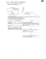


2.3.3.4. Digital Board Section
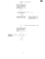
When the unit fails to boot up the system, take the troubleshooting procedures very carefully. It may have a serious problem.
The symptom: No response when the power is turned on. (No LCD display, and keys are not accepted.)
The first step is to check the power source. If there is no problem with the power supply unit, the problem may lie in the digital unit
(main board).
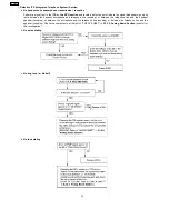
As there are many potential causes in this case (ASIC, DRAM, etc.), it may be difficult to specify what you should check first. If a
mistake is made in the order of checks, a normal part may be determined faulty, wasting both time and money.
Although the tendency is to regard the problem as a serious one (IC malfunction, etc.), usually most cases are caused by solder
faults (poor contact due to a tunnel in the solder, signal short circuit due to solder waste).
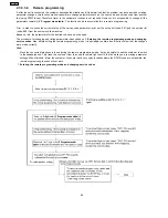
Note:
1. Electrical continuity may have existed at the factory check, but a faulty contact occurred as a result of vibration, etc., during
transport.
2. Solder waste remaining on the board may get caught under the IC during transport, causing a short circuit.
Before we begin mass production, several hundred trial units are produced at the plant, various tests are applied and any
malfunctions are analyzed. (In past experiences, digital IC (especially SRAM, DRAM and ROM) malfunctions are extremely rare
after installation in the product.)
This may be repaired by replacing the IC, (DRAM etc.). However, the real cause may not have been an IC malfunction but a
soldering fault instead.
Soldering faults difficult to detect with the naked eye are common, particularly for ASIC and RA (Resistor Array). But if you have
an oscilloscope, you can easily determine the problem site or IC malfunction by checking the main signal lines.
Even if you don’t have such a measuring instrument, by checking each main signal line and resoldering it, in many cases the
problem will be resolved.
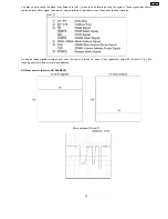
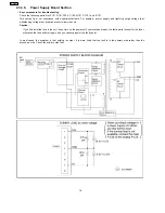
An explanation of the main signals (for booting up the unit) is presented below.
What are the main signals for booting up the unit?
Please refer to 2.3.3.4.1. Digital Block Diagram.
The ASIC (IC501) controls all the other digital ICs. When the power is turned on, the ASIC retrieves the operation code stored in
the ROM (IC502), then follows the instructions for controlling each IC. All ICs have some inner registers that are assigned to a
certain address.
It is the address bus by which the ASIC designates the location inside each IC. And the data bus reads or writes the data in order
to transmit the instructions from the ASIC to the ICs.
These signal lines are all controlled by voltages of 5V (H) or 0V (L).
63
KX-FP101
Summary of Contents for KX-FP105BX
Page 36: ...1 11 CCITT No 1 Test Chart Actual size 8 KX FP101 ...
Page 38: ...1 12 2 CONTROL PANEL 10 KX FP101 ...
Page 58: ...2 3 3 TROUBLESHOOTING ITEMS TABLE 30 KX FP101 ...
Page 59: ...2 3 3 1 Simple Check List 31 KX FP101 ...
Page 61: ...2 Document JAM 33 KX FP101 ...
Page 65: ...6 Paper JAM 7 Multiple feed and skew 37 KX FP101 ...
Page 68: ...Fig C 12 A blank page is received 40 KX FP101 ...
Page 72: ...2 3 3 3 1 Defective facsimile section 1 Transmit problem 44 KX FP101 ...
Page 80: ...52 KX FP101 ...
Page 81: ...53 KX FP101 ...
Page 82: ...54 KX FP101 ...
Page 83: ...55 KX FP101 ...
Page 84: ...56 KX FP101 ...
Page 85: ...57 KX FP101 ...
Page 86: ...58 KX FP101 ...
Page 87: ...59 KX FP101 ...
Page 92: ...2 3 3 4 1 Digital Block Diagram 64 KX FP101 ...
Page 95: ...I O and Pin No Diagram 67 KX FP101 ...
Page 97: ...69 KX FP101 ...
Page 98: ...NG Example 70 KX FP101 ...
Page 99: ...2 3 3 4 2 Check the Status of the Digital Board 71 KX FP101 ...
Page 101: ...Note Inside the digital board 73 KX FP101 ...
Page 105: ...2 Troubleshooting Flow Chart 77 KX FP101 ...
Page 107: ...2 3 3 7 Operation Panel Section 1 No key operation 2 No LCD indication 79 KX FP101 ...
Page 110: ...2 3 3 9 CIS Contact Image Sensor Section Refer to 6 4 4 SCANNING BLOCK 82 KX FP101 ...
Page 111: ...83 KX FP101 ...
Page 112: ...2 3 3 10 Thermal Head Section Refer to 6 4 3 THERMAL HEAD 84 KX FP101 ...
Page 125: ...2 4 7 3 PRINTOUT EXAMPLE 97 KX FP101 ...
Page 126: ...98 KX FP101 ...
Page 129: ...2 5 3 PRINT TEST PATTERN 1 Platen roller Reference pattern 101 KX FP101 ...
Page 130: ...2 Left margin Top margin Reference pattern 102 KX FP101 ...
Page 131: ...3 Thermal head 1 dot Reference pattern 103 KX FP101 ...
Page 154: ...6 3 2 MEMORY MAP 126 KX FP101 ...
Page 166: ...138 KX FP101 ...
Page 176: ...6 4 6 3 2 Transmitting documents 6 4 6 3 3 Receiving FAX 148 KX FP101 ...
Page 177: ...6 4 6 3 4 Copying 149 KX FP101 ...
Page 212: ...12 1 MEMO KX FP101 184 ...
Page 214: ...13 1 MEMO KX FP101 186 ...
Page 216: ...14 1 MEMO KX FP101 188 ...
Page 218: ...15 1 MEMO KX FP101 190 ...
Page 220: ...16 1 MEMO KX FP101 192 ...
Page 221: ...17 TERMINAL GUIDE OF THE IC S TRANSISTORS AND DIODES 193 KX FP101 ...
Page 222: ...18 FIXTURES AND TOOLS 194 KX FP101 ...
Page 223: ...19 CABINET MECHANICAL AND ELECTRICAL PARTS LOCATION 19 1 OPERATION PANEL SECTION 195 KX FP101 ...
Page 224: ...19 2 UPPER CABINET SECTION 196 KX FP101 ...
Page 225: ...19 2 1 PICK UP BASE SECTION 197 KX FP101 ...
Page 226: ...19 3 LOWER P C B SECTION 198 KX FP101 ...
Page 227: ...19 4 MOTOR SECTION 199 KX FP101 ...
Page 228: ...19 5 ACTUAL SIZE OF SCREWS AND WASHER 200 KX FP101 ...
Page 229: ...20 ACCESSORIES AND PACKING MATERIALS 201 KX FP101 ...