


Enhanced Modular Input/Output Subsystem (eMIOS200)
PXN20 Microcontroller Reference Manual, Rev. 1
28-50
Freescale Semiconductor
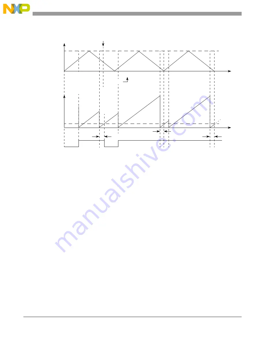
Figure 28-47. OPWMCB with 100% Duty Cycle (A1 = 4 and B1 = 3)
The output disable feature, if enabled, causes the output flip-flop to transition to the EDPOL inverted state.
This feature allows an application to force the channel output pin to a “safe” state. The internal channel
matches continue to occur even in this case, thus generating flags. As soon as the output disable is
deasserted, the channel output pin is again controlled by the A1 and B1 matches. This process is
synchronous, meaning that the output channel pin transitions on system clock edges only.
It is important to notice that, as in OPWMB and OPWFMB modes, the match signal used to set or clear
the channel output flip-flop is generated on the deassertion of the channel combinational comparator
output signal which compares the selected time base with A1 or B1 register values. Refer to
which shows the delay from matches to output flip-flop transition in OPWFMB mode. The operation of
OPWMCB mode is similar to OPWFMB regarding matches and output pin transition.
28.4.1.1.14
Pulse-Width Modulation Buffered (OPWMB) Mode
OPWMB mode is used to generate pulses with programmable leading- and trailing-edge placement. An
external counter must be selected from one of the counter buses. The A1 register value defines the first
edge and B1 defines the second edge. The output signal polarity is defined by the EDPOL bit. If EDPOL
is 0, a negative edge occurs when A1 matches the selected counter bus; and a positive edge occurs when
B1 matches the selected counter bus.
The A1 and B1 registers are double buffered and updated from A2 and B2, respectively, at the cycle
boundary. The load operation is similar to the OPWFMB mode. Refer to
for more
information about A1 and B1 registers’ update.
0x000001
0x000020
0x000004
A1 Value
A2 Value
B1 Value
B2 Value
0x000004
0x000001
Output Flip-Flop
0x000003
0x000015
0x000003
0x000015
0x000003
Selected
Counter Bus
Time
Write to B2
Time
Cycle
n
Cycle
n
+ 1
Cycle
n
+ 2
Dead-Time
Dead-Time
Dead-Time
Summary of Contents for PXN2020
Page 1: ...PXN20 Microcontroller Reference Manual Devices Supported PXN2020 PXN2120 PXN20RM Rev 1 06 2011...
Page 42: ...PXN20 Microcontroller Reference Manual Rev 1 lxiv Freescale Semiconductor...
Page 64: ...Introduction PXN20 Microcontroller Reference Manual Rev 1 1 22 Freescale Semiconductor...
Page 112: ...Signal Description PXN20 Microcontroller Reference Manual Rev 1 3 44 Freescale Semiconductor...
Page 118: ...Resets PXN20 Microcontroller Reference Manual Rev 1 4 6 Freescale Semiconductor...
Page 372: ...e200z6 Core Z6 PXN20 Microcontroller Reference Manual Rev 1 13 8 Freescale Semiconductor...
Page 412: ...e200z0 Core Z0 PXN20 Microcontroller Reference Manual Rev 1 14 14 Freescale Semiconductor...
Page 821: ...Media Local Bus MLB PXN20 Microcontroller Reference Manual Rev 1 Freescale Semiconductor 27 49...
Page 822: ...Media Local Bus MLB PXN20 Microcontroller Reference Manual Rev 1 27 50 Freescale Semiconductor...
Page 1376: ...Memory Map PXN20 Microcontroller Reference Manual Rev 1 A 118 Freescale Semiconductor...