


NXP Semiconductors
UM11759
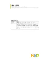
PCA9846PW-ARD evaluation board
Figure 4. PCA9846PW-ARD – I
2
C-bus switch/repeater section
4.3 Power distribution
The VDD1 power pin of PCA9846 (U11) and the VCCA power pin of PCA9617A (U7)
are supplied from VCC_LDOUT1 rail, provided by the programmable power supply
LDO 1. This configuration allows testing and measurement of the static and dynamic
characteristics of the DUT for multiple logic levels for the I
2
C-bus interface (SDA and
shows the LDO 1 circuit. The main element of the
programmable power supply is the adjustable voltage regulator LDK120MK IC (U3).
As shown in
, in the feedback loop the analog multiplexer U18 is placed in the
feedback loop of the LDO, allowing for multiple combinations of the programmable
resistors to be selected. The result is the voltage regulator can provide multiple output
voltages for the VCC_LDOOUT1 rail. The analog multiplexer is controlled from the EVK
through the Arduino port (the connector J5, pin 1, 2, and 3).
lines, logic level, and the available output voltages of the LDO 1 regulator.
UM11759
All information provided in this document is subject to legal disclaimers.
© NXP B.V. 2022. All rights reserved.
User manual
Rev. 1 — 6 June 2022
10 / 27