


External Bus Interface (EBI)
MPC5644A Microcontroller Reference Manual, Rev. 6
Freescale Semiconductor
323
14.5.2.8
Termination signals protocol
The termination signals protocol was defined in order to avoid electrical contention on lines that can be
driven by various sources. In order to do that, a slave must not drive signals associated with the data
transfer until the address phase is completed and it recognizes the address as its own. The slave must
disconnect from signals immediately after it acknowledges the cycle and not later than the termination of
the next address phase cycle.
For EBI-mastered non-chip-select accesses, the EBI requires assertion of TA from an external device to
signal that the bus cycle is complete. The EBI uses a latched version of TA (1 cycle delayed) for these
accesses to help make timing at high frequencies. This results in the EBI driving the address and control
signals 1 cycle longer than required, as seen in
. However, the DATA does not need to be held
1 cycle longer by the slave, because the EBI latches DATA every cycle during non-chip-select accesses.
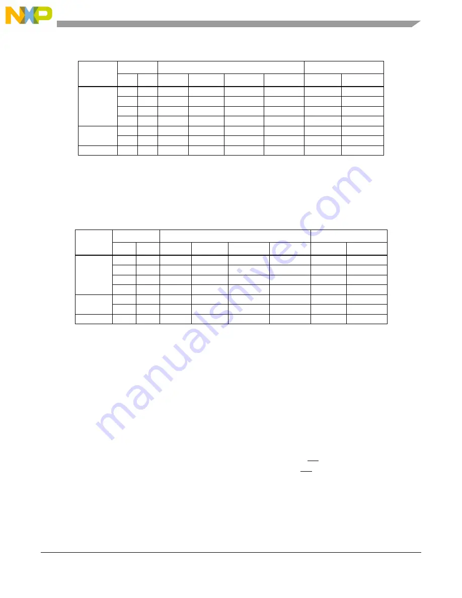
Table 14-16. Data Bus Requirements for Read Cycles
Transfer
Size
Address
32-Bit Port Size
16-Bit Port Size
1
A30
A31
D0:D7
D8:D15
D16:D23
D24:D31
D0:D7
2
D8:D15
3
Byte
0
0
OP0
—
—
—
OP0
—
0
1
—
OP1
—
—
—
OP1
1
0
—
—
OP2
—
OP2
—
1
1
—
—
—
OP3
—
OP3
16-bit
0
0
OP0
OP1
—
—
OP0
OP1
1
0
—
—
OP2
OP3
OP2
OP3
32-bit
0
0
OP0
OP1
OP2
OP3
OP0/OP2
4
OP1/OP3
1
Also applies when DBM=1 for 16-bit data bus mode.
2
For address/data muxed transfers, DATA[16:23] are used externally, not DATA[0:7].
3
For address/data muxed transfers, DATA[24:31] are used externally, not DATA[8:15].
4
This case consists of two 16-bit external transactions, the first fetching OP0 and OP1, the second
fetching OP2 and OP3.
Table 14-17. Data Bus Contents for Write Cycles
Transfer
Size
Address
32-Bit Port Size
16-Bit Port Size
1
A30
A31
D0:D7
D8:D15
D16:D23
D24:D31
D0:D7
2
D8:D15
3
Byte
0
0
OP0
—
—
—
OP0
—
0
1
—
OP1
-
—
—
OP1
1
0
—
—
OP2
—
OP2
—
1
1
—
—
—
OP3
—
OP3
16-bit
0
0
OP0
OP1
—
—
OP0
OP1
1
0
—
—
OP2
OP3
OP2
OP3
32-bit
0
0
OP0
OP1
OP2
OP3
OP0/OP2
4
OP1/OP3
1
Also applies when DBM=1 for 16-bit data bus mode.
2
For address/data muxed transfers, DATA[16:23] are used externally, not DATA[0:7].
3
For address/data muxed transfers, DATA[24:31] are used externally, not DATA[8:15].
4
This case consists of two 16-bit external transactions, the first writing OP0 and OP1, the second
writing OP2 and OP3.
Summary of Contents for MPC5644A
Page 2: ...MPC5644A Microcontroller Reference Manual Rev 6 2 Freescale Semiconductor...
Page 24: ...MPC5644A Microcontroller Reference Manual Rev 6 24 Freescale Semiconductor...
Page 26: ...MPC5644A Microcontroller Reference Manual Rev 6 26 Freescale Semiconductor...
Page 52: ...Introduction MPC5644A Microcontroller Reference Manual Rev 6 52 Freescale Semiconductor...
Page 56: ...Memory Map MPC5644A Microcontroller Reference Manual Rev 6 56 Freescale Semiconductor...
Page 1228: ...Decimation Filter MPC5644A Microcontroller Reference Manual Rev 6 1228 Freescale Semiconductor...
Page 1440: ...FlexCAN Module MPC5644A Microcontroller Reference Manual Rev 6 1440 Freescale Semiconductor...