


Universal Serial Bus Interface
MCF5253 Reference Manual, Rev. 1
24-134
Freescale Semiconductor
24.11.3.2.2
Data Toggle Inhibit
This feature is for test purposes only and should never be used during normal device controller operation.
Setting the data toggle Inhibit bit active ('1') causes the USB_DR to ignore the data toggle pattern that is
normally sent and accept all incoming data packets regardless of the data toggle state.
In normal operation, the USB_DR checks the DATA0/DATA1 bit against the data toggle to determine if
the packet is valid. If Data PID does not match the data toggle state bit maintained by the device controller
for that endpoint, the Data toggle is considered not valid. If the data toggle is not valid, the device
controller assumes the packet was already received and discards the packet (not reporting it to the DCD).
To prevent the USB_DR from re-sending the same packet, the device controller will respond to the error
packet by acknowledging it with either an ACK or NYET response.
24.11.3.3 Device Operational Model For Packet Transfers
All transactions on the USB bus are initiated by the host and in turn, the device must respond to any request
from the host within the turnaround time stated in the USB 2.0 Specification.
A USB host will send requests to the USB_DR in an order that can not be precisely predicted as a single
pipeline, so it is not possible to prepare a single packet for the device controller to execute. However, the
order of packet requests is predictable when the endpoint number and direction is considered. For example,
if endpoint 3 (transmit direction) is configured as a bulk pipe, then we can expect the host will send IN
requests to that endpoint. This USB_DR prepares packets for each endpoint/direction in anticipation of the
host request. The process of preparing the device controller to send or receive data in response to host
initiated transaction on the bus is referred to as ‘priming’ the endpoint. This term will be used throughout
the following documentation to describe the USB_DR operation so the DCD can be architected properly
use priming. Further, note that the term ‘flushing’ is used to describe the action of clearing a packet that
was queued for execution.
24.11.3.3.1
Priming Transmit Endpoints
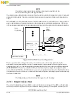
Priming a transmit endpoint will cause the device controller to fetch the device transfer descriptor (dTD)
for the transaction pointed to by the device queue head (dQH). After the dTD is fetched, it will be stored
in the dQH until the device controller completes the transfer described by the dTD. Storing the dTD in the
dQH allows the device controller to fetch the operating context needed to handle a request from the host
without the need to follow the linked list, starting at the dQH when the host request is received.
After the device has loaded the dTD, the leading data in the packet is stored in a FIFO in the device
controller. This FIFO is split into virtual channels so that the leading data can be stored for any endpoint
up to the maximum number of endpoints configured at device synthesis time.
After a priming request is complete, an endpoint state of primed is indicated in the ENDPTSTATUS
register. For a primed transmit endpoint, the device controller can respond to an IN request from the host
and meet the stringent bus turnaround time of High Speed USB.
Since only the leading data is stored in the device controller FIFO, it is necessary for the device controller
to begin filling in behind leading data after the transaction starts. The FIFO must be sized to account for
the maximum latency that can be incurred by the system memory bus.
Summary of Contents for MCF5253
Page 1: ...Document Number MCF5253RM Rev 1 08 2008 MCF5253 Reference Manual...
Page 26: ...MCF5253 Reference Manual Rev 1 xxvi Freescale Semiconductor...
Page 32: ...MCF5253 Reference Manual Rev 1 xxxii Freescale Semiconductor...
Page 46: ...MCF5253 Introduction MCF5253 Reference Manual Rev 1 1 14 Freescale Semiconductor...
Page 62: ...Signal Description MCF5253 Reference Manual Rev 1 2 16 Freescale Semiconductor...
Page 98: ...Instruction Cache MCF5253 Reference Manual Rev 1 5 10 Freescale Semiconductor...
Page 104: ...Static RAM SRAM MCF5253 Reference Manual Rev 1 6 6 Freescale Semiconductor...
Page 128: ...Synchronous DRAM Controller Module MCF5253 Reference Manual Rev 1 7 24 Freescale Semiconductor...
Page 144: ...Bus Operation MCF5253 Reference Manual Rev 1 8 16 Freescale Semiconductor...
Page 176: ...System Integration Module SIM MCF5253 Reference Manual Rev 1 9 32 Freescale Semiconductor...
Page 198: ...Analog to Digital Converter ADC MCF5253 Reference Manual Rev 1 12 6 Freescale Semiconductor...
Page 246: ...DMA Controller MCF5253 Reference Manual Rev 1 14 18 Freescale Semiconductor...
Page 282: ...UART Modules MCF5253 Reference Manual Rev 1 15 36 Freescale Semiconductor...
Page 344: ...Audio Interface Module AIM MCF5253 Reference Manual Rev 1 17 46 Freescale Semiconductor...
Page 362: ...I2 C Modules MCF5253 Reference Manual Rev 1 18 18 Freescale Semiconductor...
Page 370: ...Boot ROM MCF5253 Reference Manual Rev 1 19 8 Freescale Semiconductor...