


MCF5253 Reference Manual, Rev. 1
Freescale Semiconductor
21-1
Chapter 21
IEEE 1149.1 Test Access Port (JTAG)
This chapter discussed the JTAG signal descriptions, TAP controller, register descriptions, and how to
disable the standard operation.
The MCF5253 JTAG test architecture implementation currently supports circuit board test strategies that
are based on the IEEE standard. This architecture provides access to all of the data and chip control pins
from the board edge connector through the standard four-pin test access port (TAP) and the active-low
JTAG reset pin, TRST. The test logic uses static design and is wholly independent of the system logic,
except where the JTAG is subordinate to other complimentary test modes (see
,
”
for more information). When in subordinate mode, the JTAG test logic is
placed in reset and the TAP pins can be used for other purposes in accordance with the rules and
restrictions set forth using a JTAG compliance-enable pin.
21.1
Features
The MCF5253 JTAG implementation can do the following:
•
Perform boundary-scan operations to test circuit board electrical continuity
•
Bypass the MCF5253 by reducing the shift register path to a single cell
•
Sample the MCF5253 system pins during operation and transparently shift out the result
•
Set the MCF5253 output drive pins to fixed logic values while reducing the shift register path to a
single cell
•
Protect the MCF5253 system output and input pins from backdriving and random toggling (such
as during in-circuit testing) by placing all system signal pins to high- impedance state
NOTE
The IEEE Standard 1149.1 test logic cannot be considered completely
benign to those planning not to use JTAG capability. Users must observe
certain precautions to ensure that this logic does not interfere with system or
debug operation. Refer to
Section 21.7, “Disabling IEEE 1149.1A Standard
21.2
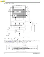
Block Diagram
is a block diagram of the MCF5253 implementation of the 1149.1A IEEE Standard. The test
logic includes several test data registers, an instruction register, instruction register control decode, and a
16-state dedicated TAP controller.
Summary of Contents for MCF5253
Page 1: ...Document Number MCF5253RM Rev 1 08 2008 MCF5253 Reference Manual...
Page 26: ...MCF5253 Reference Manual Rev 1 xxvi Freescale Semiconductor...
Page 32: ...MCF5253 Reference Manual Rev 1 xxxii Freescale Semiconductor...
Page 46: ...MCF5253 Introduction MCF5253 Reference Manual Rev 1 1 14 Freescale Semiconductor...
Page 62: ...Signal Description MCF5253 Reference Manual Rev 1 2 16 Freescale Semiconductor...
Page 98: ...Instruction Cache MCF5253 Reference Manual Rev 1 5 10 Freescale Semiconductor...
Page 104: ...Static RAM SRAM MCF5253 Reference Manual Rev 1 6 6 Freescale Semiconductor...
Page 128: ...Synchronous DRAM Controller Module MCF5253 Reference Manual Rev 1 7 24 Freescale Semiconductor...
Page 144: ...Bus Operation MCF5253 Reference Manual Rev 1 8 16 Freescale Semiconductor...
Page 176: ...System Integration Module SIM MCF5253 Reference Manual Rev 1 9 32 Freescale Semiconductor...
Page 198: ...Analog to Digital Converter ADC MCF5253 Reference Manual Rev 1 12 6 Freescale Semiconductor...
Page 246: ...DMA Controller MCF5253 Reference Manual Rev 1 14 18 Freescale Semiconductor...
Page 282: ...UART Modules MCF5253 Reference Manual Rev 1 15 36 Freescale Semiconductor...
Page 344: ...Audio Interface Module AIM MCF5253 Reference Manual Rev 1 17 46 Freescale Semiconductor...
Page 362: ...I2 C Modules MCF5253 Reference Manual Rev 1 18 18 Freescale Semiconductor...
Page 370: ...Boot ROM MCF5253 Reference Manual Rev 1 19 8 Freescale Semiconductor...