LPC5411x
All information provided in this document is subject to legal disclaimers.
© NXP Semiconductors N.V. 2018. All rights reserved.
Product data sheet
Rev. 2.1 — 9 May 2018
68 of 105
NXP Semiconductors
LPC5411x
32-bit ARM Cortex-M4/M0+ microcontroller
[6]
The maximum t
f
for the SDA and SCL bus lines is specified at 300 ns. The maximum fall time for the SDA output stage t
f
is specified at
250 ns. This allows series protection resistors to be connected in between the SDA and the SCL pins and the SDA/SCL bus lines
without exceeding the maximum specified t
f
.
[7]
In Fast-mode Plus, fall time is specified the same for both output stage and bus timing. If series resistors are used, designers should
allow for this when considering bus timing.
[8]
The maximum t
HD;DAT
could be 3.45
s and 0.9
s for Standard-mode and Fast-mode but must be less than the maximum of t
VD;DAT
or
t
VD;ACK
by a transition time. This maximum must only be met if the device does not stretch the LOW period (t
LOW
) of the SCL signal. If
the clock stretches the SCL, the data must be valid by the set-up time before it releases the clock.
[9]
tSU;DAT is the data set-up time that is measured with respect to the rising edge of SCL; applies to data in transmission and the
acknowledge.
[10] A Fast-mode I
2
C-bus device can be used in a Standard-mode I
2
C-bus system but the requirement t
SU;DAT
= 250 ns must then be met.
This will automatically be the case if the device does not stretch the LOW period of the SCL signal. If such a device does stretch the
LOW period of the SCL signal, it must output the next data bit to the SDA line t
r(max)
+ t
SU;DAT
= 1000 + 250 = 1250 ns (according to the
Standard-mode I
2
C-bus specification) before the SCL line is released. Also the acknowledge timing must meet this set-up time.
11.9 I
2
S-bus interface
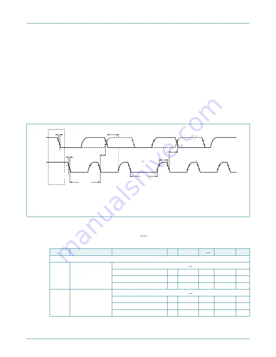
Fig 19. I
2
C-bus pins clock timing
002aaf425
t
f
70 %
30 %
SDA
t
f
70 %
30 %
S
70 %
30 %
70 %
30 %
t
HD;DAT
SCL
1 / f
SCL
70 %
30 %
70 %
30 %
t
VD;DAT
t
HIGH
t
LOW
t
SU;DAT
Table 30.
Dynamic characteristics: I
2
T
amb
=
40
C to 105
C; V
DD
= 1.62 V to 3.6 V; C
L
= 30 pF balanced loading on all pins; Input slew = 1.0 ns, SLEW setting =
standard mode for all pins; Parameters sampled at the 90 % and 10 % level of the rising or falling edge.
Symbol
Parameter
Conditions
Min
Typ
Max
Unit
Common to master and slave
t
WH
pulse width HIGH
on pins I2Sx_TX_SCK and I2Sx_RX_SCK
CCLK = 1 MHz to 12 MHz
(T
cyc
/2) -1 -
(T
cyc
/2) +1 ns
CCLK = 48 MHz to 60 MHz
(T
cyc
/2) -1 -
(T
cyc
/2) +1 ns
CCLK = 96 MHz
(T
cyc
/2) -1 -
(T
cyc
/2) +1 ns
t
WL
pulse width LOW
on pins I2Sx_TX_SCK and I2Sx_RX_SCK
CCLK = 1 MHz to 12 MHz
(T
cyc
/2) -1 -
(T
cyc
/2) +1 ns
CCLK = 48 MHz to 60 MHz
(T
cyc
/2) -1 -
(T
cyc
/2) +1 ns
CCLK = 96 MHz
(T
cyc
/2) -1 -
(T
cyc
/2) +1 ns