


MS51
Dec. 17, 2019
Page
257
of 316
Rev 1.01
M
S51
SE
RIES
TE
CHNICA
L REF
ERE
N
CE MA
NU
A
L
data in from the Slave via MISO line. The two shift registers in the Master MCU and the Slave MCU
can be considered as one 16-bit circular shift register. Therefore, while a transfer data pushed from
Master into Slave, the data in Slave will also be pulled in Master device respectively. The transfer
effectively exchanges the data, which was in the SPI shift registers of the two MCUs.
By default, SPI data is transferred MSB first. If the LSBFE (SPCR.5) is set, SPI data shifts LSB first.
This bit does not affect the position of the MSB and LSB in the data register. Note that all the following
description and figures are under the condition of LSBFE logic 0. MSB is transmitted and received
first.
There are three SPI registers to support its operations, including SPI control register (SPCR), SPI
status register (SPSR), and SPI data register (SPDR). These registers provide control, status, data
storage functions, and clock rate selection. The following registers relate to SPI function.
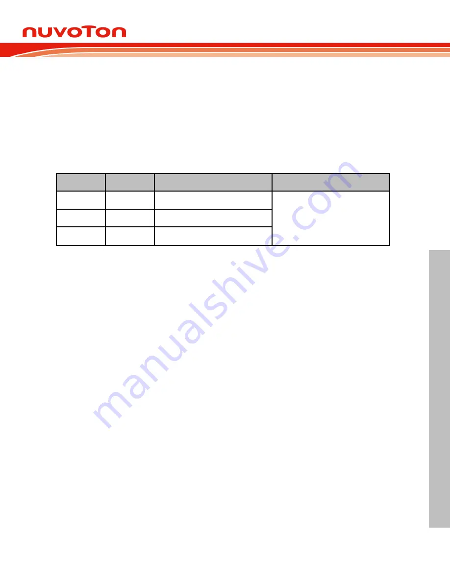
DISMODF
SSOE
Master Mode (MSTR = 1)
Slave Mode (MSTR = 0)
0
X
SS
̅̅̅̅
input for Mode Fault
SS
̅̅̅̅
Input for Slave select
1
0
General purpose I/O
1
1
Automatic
SS
̅̅̅̅
output
Table 6.9-1 Slave Select Pin Configurations
6.9.1
Operating Modes
Master Mode
6.9.1.1
The SPI can operate in Master mode while MSTR (SPInCR.4) is set as 1. Only one Master SPI device
can initiate transmissions. A transmission always begins by Master through writing to SPInDR. The
byte written to SPInDR begins shifting out on MOSI pin under the control of SPCLK. Simultaneously,
another byte shifts in from the Slave on the MISO pin. After 8-bit data transfer complete, SPIF
(SPInSR.7) will automatically set via hardware to indicate one byte data transfer complete. At the
same time, the data received from the Slave is also transferred in SPInDR. User can clear SPIF and
read data out of SPInDR.
Slave Mode
6.9.1.2
When MSTR is 0, the SPI operates in Slave mode. The SPCLK pin becomes input and it will be
clocked by another Master SPI device. The
SS
̅̅̅̅̅
pin also becomes input. The Master device cannot
exchange data with the Slave device until the
SS
̅̅̅̅̅
pin of the Slave device is externally pulled low.
Before data transmissions occurs, the
SS
̅̅̅̅̅
of the Slave device should be pulled and remain low until
the transmission is complete. If
SS
̅̅̅̅̅
goes high, the SPI is forced into idle state. If the
SS
̅̅̅̅̅
is forced to
high at the middle of transmission, the transmission will be aborted and the rest bits of the receiving
shifter buffer will be high and goes into idle state.
In Slave mode, data flows from the Master to the Slave on MOSI pin and flows from the Slave to the
Master on MISO pin. The data enters the shift register under the control of the SPCLK from the Master
device. After one byte is received in the shift register, it is immediately moved into the read data buffer
and the SPIF bit is set. A read of the SPInDR is actually a read of the read data buffer. To prevent an
overrun and the loss of the byte that caused by the overrun, the Slave should read SPInDR out and
the first SPIF should be cleared before a second transfer of data from the Master device comes in the
read data buffer.
6.9.2
Clock Formats and Data Transfer
To accommodate a wide variety of synchronous serial peripherals, the SPI has a clock polarity bit
CPOL (SPInCR.3) and a clock phase bit CPHA (SPInCR.2). Figure 6.9-4 SPI Clock Formats shows


