background image

CCS Technical Documentation

Service tools

NSB-9

Issue 1 04/03

Nokia Corporation

Page 11

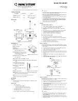
FLA-29 POS (Point Of Sale) Flash Adapter

FLA-29 POS Flash Adapter is used in place of the phone's normal battery during service, 
to supply a controlled operating voltage.

Product Code

FLA-29 POS Flash Loading Adapter:

0775306

View of FLA-29

Summary of Contents for NSB-9

Page 1: ...Customer Care Solutions Technical Documentation Issue 1 04 03 Copyright 2003 Nokia Corporation All Rights Reserved SERVICE MANUAL NSB 9 Cellular Phones NMP Part No Original 0274280 COMPANY CONFIDENTIAL ...

Page 2: ...Customer Care Solutions Technical Documentation Issue 1 04 03 Copyright 2003 Nokia Corporation All Rights Reserved Amendment Record Sheet Amendment No Date Inserted By Comments 04 2003 ViK Issue 1 ...

Page 3: ...yright 2003 Nokia Corporation All Rights Reserved Nokia NSB 9 Service Manual Structure 1 Foreword 2 General Information 3 System Module 4 Parts List 5 Service Software Instructions 6 Service Tools 7 Disassembly Instructions 8 Troubleshooting Instructions 9 Schematics ...

Page 4: ...th service bulletins While every endeavour has been made to ensure the accuracy of this document some errors may exist If any errors are found by the reader NOKIA CORPORATION should be notified in writing Please state Title of the Document Issue Number Date of publication Latest Amendment Number if applicable Page s and or Figure s in error Please send to Nokia Corporation Nokia Mobile Phones Ltd ...

Page 5: ...TAIN POTENTIALLY EXPLOSIVE ATMOSPHERES EG PETROL STATIONS SERVICE STATIONS BLASTING AREAS ETC 3 OPERATION OF ANY RADIO TRANSMITTING EQUIPMENT INCLUDING CELLU LAR TELEPHONES MAY INTERFERE WITH THE FUNCTIONALITY OF INADE QUATELY PROTECTED MEDICAL DEVICES CONSULT A PHYSICIAN OR THE MANUFACTURER OF THE MEDICAL DEVICE IF YOU HAVE ANY QUESTIONS OTHER ELECTRONIC EQUIPMENT MAY ALSO BE SUBJECT TO INTERFERE...

Page 6: ...t be applied except for the phone covers which can be replaced by the customer All electronic parts of the phone including the display are susceptible to ESD Resistors too can be damaged by static electricity discharge All ESD sensitive parts must be packed in metallized protective bags during shipping and handling outside any ESD Protected Area EPA Every repair action involving opening the phone ...

Page 7: ...CCS Technical Documentation NSB 9 Series Transceivers Issue 1 04 03 Nokia Corporation General Information ...

Page 8: ...Corporation Issue 1 04 03 Table of Contents Page No NSB 9 Product Selection 3 Accessories List 4 Technical Specifications 5 General Specifications of Transceiver NSB 9 5 Environmental conditions 6 Transceiver Features 6 Electrical Characteristics 7 ...

Page 9: ...ss is 5 and GSM1900 power class is 1 It is a true DCT 4 based transceiver with new advanced features NSB 9 Product and modules Figure 1 NSB 9 transceiver Name Module name Module code Basic transceiver NSB 9 0508623 Radio module RM9 0202046 Flip NHL 6 Flip 0262868 Flip NSB 9 Flip basic LTA 9458924 NSB 9 Flip basic CAN 9459047 Mechanics assembly parts NSB 9 HDB58 0262884 Software module basic SW SW ...

Page 10: ...lia 0675300 Mobile Charger LCH 12 0675328 Note ACP 7 ACP 8 and LCH 8 chargers are also compatible with NSB 9 Portable and Office Accessories Product code Boom Headset HDB 4 0694094 Stereo Headset HDS 3 0694093 Loopset LPS 4 0630443 DCV 14 Connectivity Stand 0273869 DT 1 Music Stand 0694119 Mobile Accessories Product code Mobile Holder MBC 13L 0650048 Swivel Mount HHS 15 0620060 Car Installation Ki...

Page 11: ...Parameter Unit Cellular System GSM850 GSM1900 RX Frequency Band GSM850 869 2 893 8 MHz GSM1900 1930 2 1989 8 MHz TX Frequency Band GSM850 824 2 848 8 MHz GSM1900 1850 2 1909 8 MHz Output Power GSM850 5 33 dBm 3 2 mW 2 W GSM1900 0 30 dBm 1 0 mW 1 W Number of RF Channels GSM850 124 GSM1900 299 Channel Spacing 200 kHz Number of TX Power Levels GSM850 15 GSM1900 16 Talk time Battery BLC 2 up to 4 5 ho...

Page 12: ...ernal antenna Internal vibra Integrated handsfree IHF Speech Codecs FR EFR AMR Real time clock RTC Pop Port TM connector Environmental condition Ambient temperature Notes Normal operation 10 o C 55 o C Specifications fulfilled Reduced performance 55 o C 65 o C Operational only for short periods Intermittent operation 20 o C 10 o C and 65 o C 80 o C Operation not guaranteed but an attempt to operat...

Page 13: ...rent Consumption Parameter Min Typical Max Unit Battery Voltage Idle 0 3 5 0 V Battery Voltage Call 0 3 4 8 V Charger Input Voltage 0 3 16 V Charging Current 850 mA Parameter Min Typical Max Unit Notes Battery Voltage 3 1 3 6 4 2 V SW cut off 3 2 V Condition Min Typical Max Unit Call GSM 850 GSM 1900 250 280 mA Idle 2 5 3 5 mA Power off 150 µA ...

Page 14: ...NSB 9 CCS Technical Documentation Page 8 Nokia Corporation Issue 1 04 03 This page left intentionally blank ...

Page 15: ...CCS Technical Documentation NSB 9 Series Transceivers Issue 1 04 03 Nokia Corporation System Module and User Interface ...

Page 16: ...nctional Description 23 Modes of Operation 23 No supply 23 Backup 23 Acting Dead 23 Active 23 Sleep mode 24 Charging 24 Power Up and Reset 24 Power up with PWR key 25 Power up when charger is connected 25 Power up when battery is connected 26 RTC alarm power up 27 A D Channels 27 FM Radio 28 FM radio audio connections 29 Keyboards 29 Engine Keyboard 29 Flip 30 Flip keyboard 30 Flip position detect...

Page 17: ...chnical Documentation System Module and User Interface NSB 9 Issue 1 04 03 Nokia Corporation Page 3 Internal Speaker 41 Integrated Hands Free 41 Memory Block 42 Security 42 Production After Sales Interface 43 ...

Page 18: ...lication Interface ALWE Background noise suppressor AMS After Market Service AMR Adaptive Multi Rate ARM Processor architecture ASIC Application Specific Integrated Circuit BB Baseband CBus Control Bus CCS Customer Care Solutions CMT Cellular Mobile Telephone MCU and DSP CPU Central Processing Unit CTSI Clocking Timing Sleep Interrupt COG Chip On Glass CSP Chip Scale Package CSTN Color Super Twist...

Page 19: ...ctromagnetic Interference ESD Electro Static Discharge EXT RF External RF FBUS Asynchronous Full Duplex Serial Bus GPRS General Packet Radio Service GSM Global System for Mobile communications HS Half Rate Speech HSCSD High Speed Circuit Switched Data IC Integrated Circuit IHF Integrated Hands Free I O Input Output IrDA Infrared Association LCD Liquid Crystal Display LDO Low Drop Out LNA Low Noise...

Page 20: ...uter PCM Pulse Code Modulation PCM SIO Synchronous serial bus for PCM audio transferring PIFA Planar Inverted F antenna PWB Printed Wiring Board RF Radio Frequency SIM Subscriber Identity Module UEM Universal Energy Management UI User Interface UPP Universal Phone Processor VCXO Voltage Controlled Crystal Oscillator VCTCXO Voltage Controlled Temperature Compensated Crystal Oscillator ...

Page 21: ...nd half of qwerty keyboard is located inside Flip TF9 is con nected to radio PWB through four 2 pole poco connectors NSB 9 has Pop Port accessory interface Both two and three wire type of chargers are supported BLC 2 Li ion battery with nominal capacity of 1000 mAh is used as main power source The Baseband blocks provide the MCU DSP external memory interface and digital con trol functions in the U...

Page 22: ...p clock A backup power supply is provided for the RTC which keeps the real time clock running when the main battery is removed The backup power supply is a rechargeable surface mounted battery capacitor type The backup time with the battery is 30 minutes minimum The analog interface between the baseband and the RF section is handled by a UEM ASIC UEM provides A D and D A conversion of the in phase...

Page 23: ...ernal microphone inputs and speaker out puts UEM also includes third microphone input which is used in NSB 9 for FM radio with IHF use Left channel Input and output signal source selection and gain control is done by the UEM according to control messages from the UPP Keypad tones DTMF and other audio tones are generated and encoded by the UPP and transmitted to the UEM for decoding An external vib...

Page 24: ...Max 4 8V Charger Input Voltage 0 3V 16V Charging current 850mA Signal Min Nom Max Note VBAT 3 1V 3 6V 4 2V charging high limit voltage 3 2V SW cut off Signal Min Nom Max Note VANA 2 70V 2 78V 2 86V Imax 80mA VFLASH1 2 70V 2 61V Sleep 2 78V 2 86V 2 95V Sleep Imax 70mA Isleep 1 5mA VFLASH2 2 70V 2 78V 2 86V Imax 40mA VSIM 1 745V 2 91V 1 8V 3 0V 1 855V 3 09V Imax 25mA Isleep 0 5mA VIO 1 72V 1 8V 1 88...

Page 25: ...egulators Signal Min Nom Max Note VR1A 4 6V 4 75V 4 9V Imax 10mA VR2 2 70V 2 61V Sleep 2 78V 2 86V 2 95V Sleep Imax 100mA VR3 2 70V 2 78V 2 86V Imax 20mA VR4 2 70V 2 78V 2 86V Imax 50mA Isleep 0 1mA VR5 2 70V 2 78V 2 86V Imax 50mA Isleep 0 1mA VR6 2 70V 2 78V 2 86V Imax 50mA Isleep 0 1mA VR7 2 70V 2 78V 2 86V Imax 45mA ...

Page 26: ...diagram Figure 2 Baseband Power Distribution Diagram Bottom Connector Battery CHACON RF Regulators Baseband Regulators 6 VR2 7 VR1A VR1B VIO VSIM VCORE VANA VFLASH1 RTC Backup battery PA Supply FM Radio SIM UPP LCD FLASH Baseband UEM Audio Amplifier VBAT IRDA VFLASH2 Accessory Regulator Vout LCD LED Driver VLED VBAT VBAT Flip ...

Page 27: ...mA 8 4mA 10 5mA Operational 3uA 6uA Stand by VDIG 2 7V 2 78V 2 86V Digital supply voltage 2 1mA 3 0mA 3 9mA Operational 11uA 19uA 26uA Stand by bus enable LOW GenIO 3 FMClk 1 4V 0 1 8V 1 88V 0 4V High Low Reference clock for FM radio module Also 6 5MHz or 13MHz can be used 32kHz Frequency GenIO 8 FMWrEn 1 4V 0V 1 8V 1 88V 0 4V High Low Write Enable GenIO 11 FMCtrlClk 1 4V 0 1 8V 1 88V 0 4V High Lo...

Page 28: ...A VR2 UEM VRF_TX Voltage 2 70 2 78 2 86 V Supply for part of transmit strip Supply for TX I Q modulators Current 65 100 mA VR3 UEM VCTCXO Voltage 2 70 2 78 2 86 V Supply for VCTCXO Current 1 20 mA VR4 UEM VRF_RX Voltage 2 70 2 78 2 86 V Supply for Hagar RX preamp mixer DTOS Noise density decades 20dB dec from 6Hz to 600Hz From f 600Hz maximum noise den sity 55nVRMS ÖHz Current 50 mA VR5 UEM VDIG V...

Page 29: ... V Supply for RF BB dig ital interface and some digital parts of RF Current 100 uA Signal name From To Parameter Input Characteristics Function Min Typ Max Unit TXP RFGenOut3 UPP PA HAGAR 1 1 3 8 1 88 V Transmitter poweramplifier enable DCN2 timing 0 0 0 4 V Load Resistance 10 220 kohm Load Capacitance 20 pF Timing Accuracy 1 4 symb ol RFBusEna1X UPP HAGAR 1 1 3 8 1 88 V RFbus enable 0 0 0 4 V Cur...

Page 30: ... 1 04 03 Data frequency 10 MHz RFBusClk UPP HAGAR 1 1 38 1 88 V RFbus clock 0 0 0 4 V Load resistance 10 220 kohm Load capacitance 20 pF Data frequency 10 MHz RESET GenI O6 UPP HAGAR 1 1 38 1 85 V Reset to Hagar 0 0 0 4 V Load capacitance 20 pF Load resistance 10 220 kohm Timing accuracy 1 4 sym bol ...

Page 31: ...60 VCTCXOGnd VCTXO UPP DC Level 0 V Ground for refer ence clock RXI RXQ HAGAR UEM Differential volt age swing static 1 35 1 4 1 45 Vpp RX baseband sig nal DC level 1 3 1 35 1 4 V TXIP TXIN UEM HAGAR Differential volt age swing static 2 23 2 48 Vpp Programmable voltage swing Programmable common mode voltage Between TXIP TXIN DC level 1 17 1 20 1 23 V Source Imped ance 200 ohm TXQP TXQN UEM HAGAR Sa...

Page 32: ...xVIO High Low Keyboard matrix column 0 P01 COL 1 0 7xVIO 0 1 8V VIO 0 3xVIO High Low Keyboard matrix column 1 P02 COL 2 0 7xVIO 0 1 8V VIO 0 3xVIO High Low Keyboard matrix column 2 P03 COL 3 0 7xVIO 0 1 8V VIO 0 3xVIO High Low Keyboard matrix column 3 P04 COL 4 0 7xVIO 0 1 8V VIO 0 3xVIO High Low Keyboard matrix column 4 P05 GenI O2 COL 5 0 7xVIO 0 1 8V VIO 0 3xVIO High Low Keyboard matrix column ...

Page 33: ...10mA Output mode 7 Vin 0V Io 0A 0 5uA Standby GND GND 0V Ground GenI O14 ENB 1 4V 0V 1 8V 1 88V 0 4V High Low Chip enable active high GenI O15 CLK 1 4V 0V 1 8V 1 88V 0 4V High Low Clock input GenI O16 DATA 1 4V 0V 1 8V 1 88V 0 4V High Low Serial data input FM RADIO L FM RADIO R Lin Rin GND Vcc Lin Rin input voltage XEAR Phone InHS Phone InIHF GND Vcc Phone in input volt age Pin Ref Signal Min Nom ...

Page 34: ...time 100ns tsdh Data hold time 4 VDDI VIO 1 72V 1 8V 1 88V Logic voltage supply Connected to VIO 5 XCS 0 8xVIO 0 VIO 0 22xVIO Logic 1 Logic 0 Chip select Active low 130ns tcss XCS low before SCLK rising edge 130ns tcsh XCS low after SCLK ris ing edge 300ns tcsw XCS high pulse width 6 SCLK 0 8xVIO 0 VIO 0 22xVIO 6 5MHz Logic 1 Logic 0 Max frequency Serial clock input 250ns tscyc Clock cycle 110ns t...

Page 35: ...ripti on Spectral range UI levels Impedance Note 1 CHARGE Charge Voltage DC 0 9V 0 85A 2 GND Charge GND 100mΩ PWB connec tor 3 ACI Accessory Control Interface 1 kbit s 0V 2 78V 47Ω Insertion removal Control 4 VOUT DC out DC 2 78V 70mA 100mΩ PWB connec tor 5 Not connected in NSB 9 6 FBUS RX 115 kbit s 0 0 86V logic 0 2 0 3 0V logic 1 33Ω 7 FBUS TX 115 kbit s 0 0 81V logic 0 1 89 2 83 V logic 1 33Ω ...

Page 36: ...1 8V SIM Card 1 6 1 8 1 9 V Supply voltage 3V SIM Card 2 8 3 0 3 2 2 SIMRST 1 8V SIM Card 0 9xVSIM 0 VSIM 0 15xVSIM V SIM reset output 3V SIM Card 0 9xVSIM 0 VSIM 0 15xVSIM 3 SIMCLK Frequency 3 25 MHz SIM clock Trise Tfall 50 ns 1 8V Voh 1 8V Vol 0 9xVSIM 0 VSIM V 3 Voh 3 Vol 0 9xVSIM 0 VSIM 4 DATA 1 8V Voh 1 8V Vol 0 9xVSIM 0 VSIM 0 15xVSIM V SIM data output 3 Voh 3 Vol 0 9xVSIM 0 VSIM 0 15xVSIM ...

Page 37: ...dition Note MICP 200mVpp AC 2 2kΩ to MIC1B 2 0 V 2 1 V 2 25 V DC MICN 2 0V 2 1V 2 25V DC Signal Min Nom Max Condition Note EARP 0 75V 0 8V 2 0 Vpp 0 85V AC DC Differential output Vdiff 4 0 Vpp EARN 0 75V 0 8V 2 0 Vpp 0 85V AC DC Signal Min Nom Max Condition Note IHFP V V Vpp V AC DC Differential output Vbat 4 1V 1kHz 8Ω 1 THD Vdiff 2 4Vpp IHFN V V Vpp V AC DC Signal Min Nom Max Condition Note VBAT...

Page 38: ...ode the backup battery has sufficient charge but the main battery can be disconnected or empty VBAT VMSTR and VBACK VBUCOFF VRTC regulator is disabled in BACKUP mode VRTC output is supplied without regulation from backup battery VBACK All the other regulators are disabled Acting Dead If the phone is off when the charger is connected the phone is powered on but enters a state called Acting Dead To ...

Page 39: ...ock counter in the UEM or by some external interrupt generated by a charger connection key press headset con nection etc In sleep mode VCTCXO is shut down and 32 kHz sleep clock oscillator is used as reference clock for the baseband Charging Charging can be performed in any operating mode The battery type size is indicated by a resistor inside the battery pack The resistor value corresponds to a s...

Page 40: ...signal is not part of the keypad matrix The power key is only connected to the UEM This means that when pressing the power key an interrupt is generated to the UPP that starts the MCU The MCU then reads the UEM interrupt register and notice that it is a PWRONX interrupt The MCU now reads the status of the PWRONX signal using the UEM control bus CBUS If the PWRONX signal stay low for a certain time...

Page 41: ...tage levels in external accessory detection inputs user interface and RF functions The monitored battery functions are battery voltage VBATADC battery type BSI and battery temperature BTEMP indication The battery type is recognized through a resistive voltage divider In phone there is a 100kOhm pull up resistor in the BSI line and the battery has a pull down resistor in the same line Depending on ...

Page 42: ...nents It has signal dependent mono stereo blend Stereo Noise Cancelling SNC The radio can tune the European US and Japan FM bands FM radio digital interface 3 wire bus contains write read clock and data lines The bus operates at maximum clock frequency of 1MHz Channel tuning and other controls are controlled through serial bus interface by the MCUSW Reference clock 32kHz is gener ated by the UPP C...

Page 43: ... FM radio audio and antenna connections Keyboards NSB 9 keyboard consists of engine keyboard and separate FLIP keyboard Flip module is connected to main PWB through 4pcs 2 pole pogo pin connectors Flip position detec tion is implemented with HALL sensor switch The switch is connected to UEM KEYB1 A D channel Magnet is located inside the flip According to the position detection parts of flip keyboa...

Page 44: ... keys 0 1 2 3 4 5 6 7 8 9 and On the other side inner side there is a half of so called qwerty keys There are 4 contacts 2 in parallel from engine to flip Supply voltage grounding clock and data lines VBAT is used as flip power supply There is a 1 8V 50mA regulator inside the flip for uController power supply Upper VBAT voltage for flip is disabled with load switch when flip is closed When the fli...

Page 45: ...er is not in use SIM Interface UEM contains the SIM interface logic level shifting SIM interface can be programmed to support 3V and 1 8V SIMs SIM supply voltage is selected by a register in the UEM It is only allowed to change the SIM supply voltage when the SIM IF is powered down The SIM power up down sequence is generated in the UEM This means that the UEM generates the RST signal to the SIM Al...

Page 46: ... Issue 1 04 03 Figure 5 UPP UEM SIM Interface Connections UEM UPP C5 C6 C7 C1 C2 C3 SIMDATA Data SIMClk SIMCLK SIMIO SIMRST VSIM From Battery Type contact SIMIO SIMClk Data GND GND SIM SIMIF register UEM digital logic BSI UIF Block CBusDa CBusEnX CBusClk C8 C4 UEMInt 100R 47R 100R 100p 27p 27p ...

Page 47: ... voltage VBAT and output is connected to System Connector VOUT pin Regulator ON OFF func tion is controlled with UPP GenI O 0 Table 25 Accessory Regulator Signals Function Notes Charging Pads for 2 wire charging in cradles Audio 4 wire fully differential stereo audio output 2 wire differential microphone input Power supply for accessories 2 78V 70mA output to accessories FBUS Standard FBUS Signal ...

Page 48: ...0 mAh Li ion battery pack BLC 2 is used in NSB 9 Table 26 BLC 2 Characteristics Description of phenomenon Volts Nominal discharge cut off voltage 3 1V Nominal battery voltage 3 6V Nominal charging voltage 4 2V Maximum charger output current 850 mA Minimum charger output current 200 mA VBAT UPP EN GenI O 0 Vout 600Ω 600Ω 600Ω 600Ω 100MHz System Connector Pin ...

Page 49: ...nning for minimum of 30 minutes Rechargeable backup battery capacitor type is connected between UEM VBACK and GND In UEM backup battery charging high limit is set to 3 2V The cut off limit voltage VBUCoff for backup battery is 2 0V Backup battery charging is controlled by MCU by writing into UEM register Battery is not charged during power off Table 28 Back up circuity Signal name Pin number Funct...

Page 50: ... 6 7 8 9 and and three in engine control keys Engine LEDs are con trolled by UEM KLIGHT and DLIGHT signals Flip LEDs are controller by flip MCU accord ing to flip serial interface messages Figure 9 Engine qwerty keypad LED connection Current through LEDs is controlled by transistor circuitry External transistor driver cir cuitry is used as constant current source in order to prevent any change in ...

Page 51: ...se or decrease the output voltage for LEDs to keep the current stable If current path through LCD LEDs is open current is at its maximum and it flows through the three other LEDs LCD NSB 9 has 130 x 130 8bpp bits per pixel passive matrix colour STN display Interface is using 9 bit data transfer D C bit is set during each transmitted byte UPP drives the CSX pin low and starts by setting the D C bit...

Page 52: ...ion or removal sequence External Audio NSB 9 is designed to support fully differential external audio accessory connection by using Pop Port system connector Pop Port connector has serial data bus called ACI Accessory Control Interface for accessory insertion and removal detection utilizing identification and authentication ACI line is also used for accessory control purposes Audio support with Po...

Page 53: ...t comparator output to change state in this case from 0 to 1 The but ton can be used for answering incoming calls and then ending them The button can be used for initiating outgoing calls if voice tags are saved for dialing Figure 11 External microphone connection UEM MICB2 MIC2P MIC2N Hookint XMICP XMICN EMC ESD Components ...

Page 54: ...ounted into the B cover Microphone is omni directional The internal microphone is connected to the UEM microphone input MIC1P N The microphone input is asymmetric and microphone bias is provided by the UEM MIC1B The microphone input on the UEM is ESD protected Spring contacts are used to connect the microphone contacts to the main PWB Figure 13 Internal microphone connections 100nF UEM MICB1 MIC1N...

Page 55: ... activated internal microphone is used as in HP mode and IHF speaker is used instead of earpiece The FM radio can be listened from the IHF speaker as well if a headset is connected FM radio antenna The stereo audio amplifier supports four inputs and three outputs It is capable of deliv ering 340mW of continuous averahe power into a mono 8Ohm bridged tied load and 25mW per channel of continuous ave...

Page 56: ...d it is byte addressable RAM is mainly for MCU purposes but also DSP has also access to it if needed MCU code is stored into external flash memory which is in a combo memory chip The size of the flash is 128Mbit 8M x 16bit The NSB 9 baseband supports a burst mode flash with multiplexed address data bus Access to the flash memory is performed as 16 bit access The flash has Read While Write capabili...

Page 57: ...duction trouble shooting purposes The standard 5 pin test pattern is shown in figure below NSB 9 has two pins for FM radio testing The pins are connected in parallel with two system connector audio output lines HSEAR P and HSEAR R N The FM radio can be tested between those lines Figure 16 Flash and FM radio test connection FBUS_RX FBUS_TX VPP MBUS GND FM Radio test audio output FM Radio test audio...

Page 58: ...NSB 9 System Module and User Interface CCS Technical Documentation Page 44 Nokia Corporation Issue 1 04 03 This page intentionally left blank ...

Page 59: ...CCS Technical Documentation NSB 9 Series Transceivers Issue 1 04 03 Nokia Corporation Parts List ...

Page 60: ...NSB 9 Parts List CCS Technical Documentation Page 2 Nokia Corporation Issue 1 04 03 Table of Contents Page No Exploded View of NSB 9 3 Mechanical parts list 4 Variant Parts 5 Parts list NSB 9 6 ...

Page 61: ...CCS Technical Documentation Parts List NSB 9 Issue 1 04 03 Nokia Corporation Page 3 Exploded View of NSB 9 RM9 Radio Module ...

Page 62: ... MODULE I013 1 XXXXXXX LCD METAL FRAME I014 1 XXXXXXX EARPIECE I015 1 4850265 LCD MODULE 128X128 COF COLOURSTN I016 1 9460432 LIGHTGUIDE NHL 6 I017 1 9795104 DOME SHEET MAINPWB I018 1 XXXXXXX RM9 RADIO MODULE 1 9510948 Lid for BB shield 1 0660274 ANTENNA WITH IHF I019 1 XXXXXXX ANTENNA I020 1 XXXXXXX INTERNAL HANDSFREE SPEAKER I021 1 9452186 VOLUME KEY I022 1 5400243 DC JACK 3 5MM I023 1 5140265 M...

Page 63: ...mod Basic LTA 9452172 BATTERY COVER Nokia Basic variant 9459050 BATTERY COVER AWS variant 9459054 BATTERY COVER T Mobile variant 9459051 BATTERY COVER Cingular variant 9459053 BATTERY COVER Rogers AT T variant 9459052 BATTERY COVER Microcell variant I011 9790747 Keymat right Common Eng DMC05411 9790863 Keymat right Spanish 9790861 Keymat ritgh Can ITEM CIRCUIT REF QTY PART NO PART NAME ...

Page 64: ... 5 S 9 RW 8 KLSFDS 13 S 9 RW 8 KLSFDS 13 S 9 RW 9 KLSFDS S 13 S 9 RW 9 KLSFDS S 13 S 9 RW 9 KLSFDS S 13 S 9 RW 9 KLSFDS S 13 S 9 RW 8 KLSFDS 13 S 9 RW B B3 3 55 13 3 9 S 9 RW 6 KLSFDS 5 9 Q 9 RW 6 KLSFDS 5 9 Q 9 RW 7 KLSFDS 5 9 Q 9 RW 7 KLSFDS 5 9 Q 9 RW 2 B B3 B 9 3 55 5 1 0 9 Q 9 RW 2 KLSFDS 5 9 Q 9 RW 2 KLSFDS 5 9 Q 9 RW 8 KLSFDS 13 S 9 RW 3 3 3 5 1 9 Q 9 RW 3 3 3 5 8 9 X 9 RW 3 3 5 1 9 Q 9 RW ...

Page 65: ... 9 Q 9 RW 0 3 3 5 1 9 Q 9 RW 0 3 3 5 1 9 Q 9 7RS KLSFDS 13 S 9 7RS KLSFDS 13 S 9 RW 0 3 3 5 1 9 Q 9 RW 3 3 5 8 9 X 9 RW KLSFDS 5 9 Q 9 RW 3 3 5 8 9 X 9 RW 2 3 3 5 8 9 X 9 RW 3 3 5 8 9 X 9 RW 3 3 5 8 9 X 9 RW 3 3 5 8 9 X 9 RW 1 3 3 5 8 9 X 9 RW KLSFDS 13 S 9 RW KLSFDS 13 S 9 RW 4 3 3 5 8 9 X 9 RW 3 3 5 8 9 X 9 RW 3 3 5 8 9 X 9 RW 3 3 5 8 9 X 9 RW 3 3 5 8 9 X 9 RW 3 3 5 1 9 Q 9 RW 1 3 3 5 8 9 X 9 RW...

Page 66: ...RW 3 3 5 1 9 Q 9 RW KLSFDS 5 9 Q 9 RW KLSFDS 5 9 Q 9 RW KLSFDS 5 9 Q 9 RW 3 3 5 8 9 X 9 RW 3 3 5 8 9 X 9 RW 3 3 5 8 9 X 9 RW 3 3 5 8 9 X 9 RW 3 3 5 8 9 X 9 RW 3 3 5 8 9 X 9 RW 3 3 5 8 9 X 9 RW 3 3 5 8 9 X 9 RW KLSFDS 13 S 9 RW 3 3 5 8 9 X 9 7RS 1 KLSFDS 13 S 9 7RS 3 3 5 1 9 Q 9 RW 5 3 3 5 8 9 X 9 RW KLSFDS 13 S 9 7RS KLSFDS S 13 S 9 S S 7RS KLSFDS S 13 S 9 S S 7RS KLSFDS S 13 S 9 S S 7RS 1 KLSFDS ...

Page 67: ...9 RW 2 KLSFDS 5 9 Q 9 RW 3 KLSFDS 13 S 9 RW 3 KLSFDS 13 S 9 RW 5 KLSFDS 13 S 9 RW 6 KLSFDS 13 S 9 RW 6 KLSFDS 13 S 9 RW 6 3 3 5 1 9 Q 9 RW 0 KLSFDS 5 9 Q 9 RW 3 3 5 1 9 Q 9 RW 0 KLSFDS 5 9 Q 9 RW KLSFDS 5 9 Q 9 RW KLSFDS 5 9 Q 9 RW 0 KLSFDS 5 9 Q 9 RW KLSFDS 13 S 9 RW 2 KLSFDS 13 S 9 RW KLSFDS 13 S 9 RW 2 KLSFDS 5 9 Q 9 RW 2 3 3 5 1 9 Q 9 RW 3 B 0 3 3 5 1 9 Q 9 RW KLSFDS S 13 S 9 S S RW KLSFDS 13 ...

Page 68: ...3 3 5 8 9 X 9 RW 3 3 5 1 9 Q 9 RW KLSFDS 13 S 9 RW KLSFDS 13 S 9 RW 3 3 5 1 9 Q 9 RW KLSFDS 5 9 Q 9 RW 3 3 5 1 9 Q 9 RW KLSFDS 5 9 Q 9 RW KLSFDS 13 S 9 RW KLSFDS 13 S 9 RW KLSFDS 13 S 9 RW 3 3 5 8 9 X 9 RW 3 3 5 8 9 X 9 RW 3 3 5 8 9 X 9 RW 3 3 5 8 9 X 9 RW 3 3 13 3 9 S 9 RW 3 3 13 3 9 S 9 RW 3 3 13 3 9 S 9 RW 3 3 13 3 9 S 9 RW KLSFDS S 13 S 9 S S RW KLSFDS 5 9 S 9 RW B 9 3 3 13 1 9 Q 9 RW 3 3 13 3...

Page 69: ...Q 9 RW KLSFDS S 13 S 9 S S RW KLSFDS 5 9 Q 9 RW KLSFDS 13 S 9 RW KLSFDS 13 S 9 RW KLSFDS 5 9 Q 9 RW KLSFDS 5 9 Q 9 RW KLSFDS S 13 S 9 S S RW KLSFDS 13 S 9 RW KLSFDS 5 9 Q 9 RW KLSFDS S 13 S 9 S S RW KLSFDS 13 S 9 RW KLSFDS 5 9 Q 9 RW KLSFDS 13 S 9 RW 3 3 13 1 9 Q 9 RW KLSFDS 13 S 9 RW KLSFDS 13 S 9 RW KLSFDS 13 S 9 RW KLSFDS 13 S 9 RW KLSFDS 13 S 9 RW KLSFDS 13 S 9 RW 0 X 8 0 2 1 72 7 a a a RW 0 X...

Page 70: ... 7 5 5 0 5 0 a a RW 8 55 7 B 55 7 5 5 0 5 0 a a RW 8 55 7 B 55 7 5 5 0 5 0 a a RW 8 55 7 B 55 7 5 5 0 5 0 a a RW 7 2 B 4 3 2 1 4 0 Q a RW 8 55 7 B 55 7 5 5 0 5 0 a a 7RS B B0 76 8 3 55 5 5 0 a RW 2 B 6 3 2 1 4 0 Q a RW 2 B 6 3 2 1 4 0 Q a RW B 0 55 7 5 5 0 5 0 a a RW B 0 55 7 5 5 0 5 0 a a RW B 0 55 7 5 5 0 5 0 a a RW B 0 55 7 5 5 0 5 0 a a RW B 0 55 7 5 5 0 5 0 a a RW B 0 55 7 5 5 0 5 0 a a RW 2 ...

Page 71: ...a Q Q RW 3 2 1 1 4 0 Q a Q Q RW 3 2 1 1 4 0 Q a Q Q RW 3 2 1 1 4 0 Q a Q Q RW 3 2 1 4 0 Q a RW 3 2 1 1 4 0 Q a Q Q RW 3 2 1 1 4 0 Q a Q Q RW B32 3 2 1 4 0 Q a RW 3 2 1 1 4 0 Q a Q Q RW 3 2 1 1 4 0 Q a Q Q RW B 0 55 5 5 0 5 0 a a RW 3 2 1 1 4 0 Q a Q Q RW 3 2 1 1 4 0 Q a Q Q RW 283 5B 5 28 5 0 a a 0 RW 9 9 5 B0B 1 1 9 5 66 9 0 530 a a a 1 RW 8 627 B B 5 9 0 3 627 a 9 a 1 RW 0 860 B67B1 6 03 0 9 0 7...

Page 72: ...0 9 9 9 9 9 a 5 RW 7 B9 5 3 9 5 6725 9 0 9 9 9 9 9 a 5 RW 9 5 5HVLVWRU P N a 5 7RS B9 5 3 9 5 6725 9 0 9 9 9 9 9 a 5 7RS B9 5 3 9 5 6725 9 0 9 9 9 9 9 a 5 RW 3 015 5 6 1 7 25 N N a a 5 RW 3 5 5HVLVWRU P N a 5 RW 5 5HVLVWRU P N a 5 RW 2 5 5HVLVWRU P N a 5 RW 3 5 5HVLVWRU P N a 5 RW 2 015 5 6 1 7 25 N N a a 5 RW 7 B9 5 3 9 5 6725 9 0 9 9 9 9 9 9 5 RW 8 B9 5 3 9 5 6725 9 0 9 9 9 9 9 9 5 RW B 9 5 6725...

Page 73: ... P 5 a 5 7RS B9 5 3 9 5 6725 9 0 9 9 9 9 9 a 5 7RS 5 5HVLVWRU P 5 a 5 7RS 5 5HVLVWRU P 5 a 5 RW 0 5 5HVLVWRU P 5 a 5 RW 5 5HVLVWRU P 5 a 5 RW B5 35 6 5 5 a 5 RW 4 5 5HVLVWRU P N a 5 RW 4 5 5HVLVWRU P N a 5 RW 3 5 5HVLVWRU P N a 5 RW 4 B5B65 5 6 1 7 25 N a 5 RW 2 5 5HVLVWRU P N a 5 RW 2 5 5HVLVWRU P N a 5 RW 6 5 5HVLVWRU P 5 a 5 RW 5 5 5HVLVWRU P 5 a 5 RW 5 5 5HVLVWRU P 5 a 5 RW 5 5HVLVWRU P 5 a 5 ...

Page 74: ...HV 5 5 a 5 RW 5 KLSUHV 5 5 a 5 RW 5 KLSUHV MXPSHU 5 a 5 RW 5 5HVLVWRU P 5 a 5 RW 5 5HVLVWRU P 5 a 5 RW 5 5HVLVWRU P 5 a 5 RW 5 5HVLVWRU P N a 5 RW 5 5HVLVWRU P N a 5 RW 5 5HVLVWRU P N a 5 RW 5 5HVLVWRU P 5 a 5 RW 5 5HVLVWRU P 5 a 5 RW 5 5HVLVWRU P N a 5 RW 5 5HVLVWRU P N a 5 RW 5 5HVLVWRU P 5 a 5 RW 5 5HVLVWRU P 5 a 6 RW 6 7 B6 5 60 7 7 6 6 75 9 00 a a a 6 RW 6 7 B6 5 60 7 7 6 6 75 9 00 a a a 7 RW...

Page 75: ...5 62 a a a 9 RW 4 62 B 3 7 0 5 62 a a a 9 RW 627 B5 75 0 5525 6 627 a a a 9 RW 627B 75 1 627 a a a 9 RW 627 6 606 9 3 627 a a a RW 211B 7B 60 77 5 211 32 635 9 a a a RW 21B B 5 211 00 32 635 a a a RW 6 6 21B04 B1 B 5 60 6 67 0 211 725 32 a a a 7RS 211B B 60 211 3 635 1 3 a a a RW 6 6 0B5 5B 6 0 5 5 5 32 3 60 a a a RW B 6 3 0 0 1 a a a 7RS 1 X 0 6 7 0 a a a RW 17B6 B 0B 6 17 6 0 0 a a RW 7 5B6 B 6 ...

Page 76: ...NSB 9 Parts List CCS Technical Documentation Page 18 Nokia Corporation Issue 1 04 03 This page intentionally left blank ...

Page 77: ...CCS Technical Documentation NSB 9 Series Transceivers Draft 1 02 03 Copyright Nokia All rights reserved Service Software Instructions ...

Page 78: ...NSB 9 Service Software Instructions CCS Technical Documentation Page 2 Copyright Nokia All rights reserved Draft 1 02 03 This page left intentionally blank ...

Page 79: ...ng the Flash Support Files 23 How to Update The FPS 8 Flash Prommer SW 26 FPS 8 Activation and Deactivation 28 Activation 28 Deactivation 30 JBV 1 Docking Station SW 31 Before Installation 31 Installing SW Needed for the JBV 1 SW Update 32 Updating the JBV 1 Docking Station Software 36 Receiver tuning Quick Guide for Tuning With Phoenix 39 General remarks 39 RF Tuning and Calibration Instructions ...

Page 80: ...NSB 9 CCS Technical Documentation Page 2 Copyright Nokia All rights reserved Issue 1 04 03 ...

Page 81: ...and flash update package Manage connection settings depends on the tools you are using Update FPS 8 SW if you use FPS 8 Activate FPS 8 Update JBV 1 Docking Station SW only when needed The flash update files are delivered with then Phoenix Data Package so unless you want to use certain version of this package separate installation package is not needed any more If you want to use it it should be in...

Page 82: ...ble to install Phoenix depending on the Operating System If the dongle driver is installed or updated you need to reboot your PC before the installation can continue If uninstalling or rebooting is needed at any point you will be prompted by the Install Shield program If at any point during installation you get this message Dongle is not found and installa tion can t continue Possible reasons may ...

Page 83: ...the phoenix_service_sw_a3_03_83_005 exe to start installation When you choose Next the files needed for installation will be extracted Kindly wait If the setup files are already extracted left in the file system from previous installation following dialog appears Always click Yes to All to overwrite the existing setup files ...

Page 84: ...Dongle driver installation will take place If the Dongle driver is installed and it is older than the latest supported version the latest version will be installed when you choose Yes The latest version is always included in the latest Phoenix installation package PC needs to be rebooted before installation can continue Click Yes to reboot the PC Setup is restarted automatically after reboot ...

Page 85: ...ngle driver installation update if needed installation continues from this step Click Next in Welcome dialog to continue Choose the destination folder it is recommended to use the default folder C Program Files Nokia Phoenix Choose Next to continue You may choose another location by selecting Browse not recommended Setup copies the components please wait ...

Page 86: ...hown Please wait If restarting of your computer is needed the Install Shield Wizard will tell you about it Select Yes to reboot the PC immediatelly and No to reboot the PC manually Note that Phoenix doesn t work if components are not registered Click Finish to continue After the reboot components are registered and Phoenix is ready for use ...

Page 87: ... after copying them If restarting of your computer is not needed Click Finish to exit the setup Phoenix is now ready for use Now the installation of Phoenix Service SW is ready and it can be used after Installing Phone model specific Phone Data Package for Phoenix Configuring the connections Updating the Flash Update Package files used with FPS 8 and FLS 4 tools ...

Page 88: ...n installing it for the first time Download the installation package to your computer hard disk Close all other programs Run the application file e g phoenix_service_sw_a3_03_83_005 exe Dongle driver version will be checked and if need be updated After reboot installation starts automatically Newer version of Phoenix will be installed When you update the Phoenix from old to new version e g update ...

Page 89: ... Copyright Nokia All rights reserved Page 13 How to Uninstall Phoenix Uninstallation can be done manually from Windows Control Panel Add Remove Pro grams Choose Phoenix Service Software and click Add Remove Choose OK to uninstall Progress of the uninstallation is shown ...

Page 90: ...ll rights reserved Issue 1 04 03 You may have to reboot the PC after uninstallation If restarting is not needed the following dialog will appear Note If you have different product packages installed components are uninstalled only if they are not included in other product packages ...

Page 91: ... Service SW Download the installation package e g NSB 9_dp_1 00 exe to your computer e g C TEMP Close all other programs Run the application file e g NSB 9_dp_1 00 exe and follow instructions on the screen If you already have the Phoenix Service SW installed on your computer sooner or later there will be need to update it when new versions are released Please note that very often the Phoenix Servi...

Page 92: ... 1 04 03 Installation of Phoenix Data Package Product Specific Run the NSB 9_dp_v_1 00 exe to start installation When you choose Next the files needed for installation will be extracted Please wait Choose Next to continue From this view you can see the contents of the Data Package Read the text carefully ...

Page 93: ... There should be information about the Phoenix version needed with this data package Choose Next Confirm location and choose Next to continue Install Shield checks where the Phoenix application is installed and the directory is shown Choose Next to continue Phone model specific files will be installed please wait ...

Page 94: ...onfidential CCS Technical Documentation Page 18 Copyright Nokia All rights reserved Issue 1 04 03 Choose Finish to complete installation You now have all phone model specific files installed in your Phoenix Service SW ...

Page 95: ... Data Package If you try to install the same version of Phoenix Data Package that you already have you are asked if you want to uninstall the version you have on your PC Answer OK to unin stall Cancel if you don t want to uninstall Older versions of data packages do not need to be uninstalled Once the previously installed Data package is uninstalled choose Finish Run the NSB 9_dp_v_1 00 exe again ...

Page 96: ...ervice SW and Login Choose Manage Connections From File Menu Existing connections can be selected edited deleted and new ones created by using this dialog A connection can be created either manually or by using a Connection Wizard To add new connection choose Add and select if you want to create it manually or by using the Wizard Choose Next to continue ...

Page 97: ...ion settings Media FBUS COM Port Virtual COM Port used by FLS 4 Please check this always To check please go to Windows Control Panel FLS Virtual Port Configuration B For FPS 8 Flash Prommer choose following connection settings Media FPS 8 Port Num COM Port where FPS 8 is connected COMBOX_DEF_MEDIA FBUS Choose Finish to complete If you use the Wizard connect the tools and a phone to your PC and the...

Page 98: ... can be used after closing the Manage Connections window Selected connection will be shown on the right hand bottom corner of the screen To use the selected connection connect the phone to Phoenix with correct service tools make sure that it is switched on and select Scan Product When the Product is found Phoenix will load product support and when everything is ready name of the loaded product sup...

Page 99: ...les are delivered in the same installation package with Phoenix data package Normally it is enough to install the data package only before updating the FPS 8 Separate installation package is for flash support files are available and the files can be updated according to this instruction Installing the Flash Support Files Start by double clicking eg flash_update_02_10_00 exe Installation begins If ...

Page 100: ...er ones the setup will be aborted If you really want to downgrade uninstall newer files manually from Control Panel and then rerun the installation again If an older version exists on your PC and it needs to be updated choose Next to con tinue installation It is highly recommended to install the files to the default destination folder C Program Files Nokia Phoenix ...

Page 101: ...04 03 Copyright Nokia All rights reserved Page 25 Choose Next to continue You may choose another location by selecting Browse not recommended Installation continues Choose Finish to complete procedure FLS 4 can be used right after Flash Update Package is installed ...

Page 102: ...NSB 9 Company confidential CCS Technical Documentation Page 26 Copyright Nokia All rights reserved Issue 1 04 03 FPS 8 must be updated by using Phoenix ...

Page 103: ... to Update The FPS 8 Flash Prommer SW Start Phoenix Service Software Select FPS 8 FPS 8C maintenance from Flashing menu When new FPS 8 flash update package is installed to computer you will be asked to update the files to your FPS 8 Prommer Select Yes to update files Update procedure takes a couple of minutes 02 0 0 ...

Page 104: ... updated by pressing Update button and selecting appropriate fps8upd ini file under C Program Files Nokia Phoenix Flash directory All files can be loaded separately to FPS 8 To do this just press right mouse button in Flash box files window and select file type to be loaded More information and help can be found from the Help dialog ...

Page 105: ...ivated Activation Before FPS 8 can be successfully used for phone programming it must be first activated Fill in first FPS 8 activation request sheet in the FPS 8 sales package and follow the instructions in the sheet When activation file is received e g 00000 in copy it to C Program Files Nokia Phoenix BoxActivation Directory on your computer This directory is created when Phoenix is installed St...

Page 106: ...t Nokia All rights reserved Issue 1 04 03 The activation file you saved to C ProgramFiles Nokia Phoenix BoxActivation directory will be shown e g 00000 in check that it is correct Box will be activated when you choose Open Turn FPS 8 power off and on to complete activation ...

Page 107: ...All rights reserved Page 31 Deactivation Start Phoenix Service Software Select FPS 8 FPS 8C maintenance from Flashing menu Select Deactivate from the FPS8 8C Maintenance UI Confirm Deactivation by choosing Yes Box will be deactivated Turn FPS 8 power off and on to complete deactivation ...

Page 108: ...t service functions The JBV 1 Docking Station contains Software Firmware which can be updated You need the following equipment to be able to update JBV 1 software PC with USB connection Operating System supporting USB Not Win 95 or NT USB Cable Can be purchased from shops or suppliers providing PC hardware and accessories JBV 1 Docking Station External Power Supply 11 16V Before Installation Downl...

Page 109: ...DO NOT CONNECT THE USB CABLE JBV 1 TO YOUR COMPUTER YET Run Jbv1_update zip file and start SW Installation by double clicking Setup exe Files needed for JBV 1 Package setup Program will be extracted Installation begins please read the information shown and Choose Next to continue Use suggested destination folder where JBV 1 SW Package will be installed and choose ...

Page 110: ...S Technical Documentation Page 34 Copyright Nokia All rights reserved Issue 1 04 03 Next to continue Select Full Installation and choose Next to continue Program Folder will be created Choose Next to continue Software files will be ...

Page 111: ...Issue 1 04 03 Copyright Nokia All rights reserved Page 35 installed After successful installation choose Finish to complete NOW YOU CAN CONNECT THE USB CABLE JBV 1 TO YOUR COMPUTER Connect power to JBV 1 11 16V DC from external power supply then connect USB ...

Page 112: ...hts reserved Issue 1 04 03 Cable between JBV 1 USB connector and PC Windows will detect connected USB cable and detect drivers for new HW Follow the instructions and allow Windows to search and install the best drivers avail able After this procedure the actual JBV 1 SW update can begin ...

Page 113: ...E and start JBV 1 Update SW by double clicking fwup exe JBV 1 Firmware update starts and shows current status of the JBV 1 connected If firmware version read from your JBV 1 is not the latest one available it needs to be updated by choosing Update Firmware Choose file JBV1v11 CDE example used here is for v 11 and Open to update your JBV 1 After Successful update current JBV 1 status will be shown ...

Page 114: ...NSB 9 Company confidential CCS Technical Documentation Page 38 Copyright Nokia All rights reserved Issue 1 04 03 software of your JBV 1 docking station and it is ready for use ...

Page 115: ...CCS Technical Documentation Company confidential NSB 9 Issue 1 04 03 Copyright Nokia All rights reserved Page 39 This page left intentionally blank ...

Page 116: ...NSB 9 Company confidential CCS Technical Documentation Page 40 Copyright Nokia All rights reserved Issue 1 04 03 ...

Page 117: ... baseband tunings are needed they should be completed before the RF tunings Avoid unnecessary tuning factory tuning values are always the most accurate ones Screen shots described in this document may change as the service software is devel oped Kindly refer to the Phoenix help files the phone model specific service manual and bulle tins for help ...

Page 118: ...ne component the product is tuned automatically Manual tuning is not available RF tunings must be performed if any RF components are changed RF tunings shall be done using MJS 48 module jig MJS 48 jig loss figures can be found from RF Service Tools chapter MJF 32 with a coupler is not allowed to use for RF tuning purpose EQUIPMENT NEEDED NSB 9 module jig MJS 48 power and DAU 9S cables DC power sup...

Page 119: ...CCS Technical Documentation NSB 9 Issue 1 04 03 Copyright Nokia All rights reserved Page 41 Figure 1 RF tuning concept Figure 2 Setup environment ...

Page 120: ...ue 1 04 03 Autotuning The Autotune component can be found under Tuning menu Figure 3 Autotune menu in Phoenix When tuning one only needs to click the Tune button to start automatic tuning proce dure Figure 4 Autotune menu RX TX menu The tuning results are shown in RX and TX windows ...

Page 121: ...u tune the phone with Phoenix using Auto Tune component When you measure the losses you have to be very careful because these values affect directly how well the phone is tuned Note Components are protected by PKD 1CS PKD 1NS PKD 1 and PKD 1P dongles using standard TSS protection procedure Autotuning itself is possible with all these dongles but with PKD 1P and PKD 1 dongles user is not able to se...

Page 122: ...irst measurement is a reference measure ment where the TXC signal is routed directly to the RXQ line without going through any filter The remaining 5 measurements are all done on first order low pass filters with a nominal corner frequency of 67 71 kHz This means that the received signal on the RXQ line ideally will have an amplitude of 0 707 times the amplitude of the TXC Saved tuning values are ...

Page 123: ...ifferent value RX I Q fre quency is measured again and AFC SLOPE frequency change divided by AFC value change is calculated GSM850 and GSM1900 RX chains gain are tuned at middle channel Table 2 RX Calibration Limits RX AM Suppression Calibration Description Calibrates GSM850 and GSM1900 RX mixer local signal DC levels to achieve best rejec tion for AM modulated interferences Calibration needs exte...

Page 124: ...ch item RX Band Filter Response Compensation Description Calibrates GSM850 and GSM1900 RX chain gain over whole band Calibration needs external signal applied to the receiver Calibration is done in 9 frequencies Table 3 RX Band Filter Response Compensation Limits Band GSM850 GSM1900 Item Typical value Low limit High limit Typical value Low limit High limit RSSI 110 85 140 80 110 90 140 80 LOP_I 0 ...

Page 125: ... Issue 1 04 03 Copyright Nokia All rights reserved Page 47 ch 190 661 0 5 1 0 5 5 0 4 0 9 5 5 ch 217 736 0 1 0 7 5 5 0 3 0 3 5 5 ch 241 794 0 7 0 1 5 5 0 9 0 0 5 5 ch 251 810 1 2 0 3 5 5 1 0 0 0 5 5 ch 261 835 1 8 0 8 10 5 2 1 0 7 10 5 ...

Page 126: ...hannel middle channel at 25 C tem perature GSM850 GSM1900 Power Level Target value Tuning target Testing limits Power Level Target value Tuning target Testing limits 5 32 5 0 1 0 2 0 5 0 29 5 0 1 0 2 0 5 6 31 0 5 1 1 28 0 5 1 7 29 0 5 1 2 26 0 5 1 8 27 0 5 1 3 24 0 5 1 9 25 0 5 1 4 22 0 5 1 10 23 0 5 1 5 20 0 5 1 11 21 0 5 1 6 18 0 5 1 12 19 0 5 1 7 16 0 5 1 13 17 0 5 1 5 8 14 0 5 1 14 15 0 5 1 5 ...

Page 127: ... I channel DC offset TX Q channel DC offset Amplitude difference between TX I and Q channels Phase difference between TX I and Q channels Tuning correctness is checked by measuring TX output spectrum at frequencies TX IQ f0 TX IQ f0 67 71 kHz Table 4 TX IQ Tuning Limits Band GSM850 GSM1900 Item Typical value Low limit High limit Typical value Low limit High limit TX I DC offset 2 1 6 6 3 1 6 6 TX ...

Page 128: ...Concept For Baseband Tuning Operations EM calibrations should be carried out in JBV 1 Docking Station equipped with MJF 32 Docking Station Adapter Power to JBV 1 should be supplied from an external DC power suply not FPS 8 prommer JBV 1 input voltages Maximum 16 VDC Nominal input for BB tunings is 12 V DC ...

Page 129: ... code 1 Docking station JBV 1 0770298 2 Docking station adapter MJF 32 0770528 3 DC DC cable SCB 3 0730114 4 RF antenna cable XRF 1 0730085 5 DC power cable PCS 1 0730012 6 Service MBUS cable DAU 9S 0730108 7 Software protection key PKD 1 0750018 8 Phoenix Service SW 8409031 Phoenix Service SW CD ROM 0775311 NSB 9 Flash SW data 8415951 NSB 9 Flash SW data CD ROM 0775344 ...

Page 130: ...paration for EM Calibration Connect DC Cable SCB 3 between JBV 1 and charger socket of Phone for Charger cali bration Connect 12 15 V from Power Supply to JBV 1 NOTE Check that connection is F BUS does not work with M BUS Select Maintenance Tuning Energy Management Calibration Energy Management values to be calibrated are checked Select Read from Phone to show the current values in the phone memor...

Page 131: ...ttery Temperature etc are saved Close the Energy Management Calibration dialog to end tuning You must manually switch the phone on after exiting Energy Management Calibration dialog Parameter Min Max Note ADC gain 25400 29000 VBatt BSI BTemp DC offset 100 100 ADC voltage offset BSI gain 860 1180 ADC BSI calibration gain BTEMP gain 1980 2280 ADC BTEMP calibration gain VBAT gain 10000 11000 ADC VBAT...

Page 132: ...rable difference in the contrast Select Maintenance Testing Display Tune Move the Contrast factory offset slider to reach good LCD contrast Both sliders are relative The Default button resets the bottom Contrast factory offset slider to default value 41 The Contrast offset slider should always be set to 0 mid dle of the scale because that setting is visible on the phone screen Close the Display tu...

Page 133: ...Setup Instructions POS Point of Sale Flash Concept Figure 1 POS flash Item Type Description Code 1 FLA 29 Point Of sales flash loading adapter 0775306 2 XCS 1 Service cable 0730218 3 ACF 8 AC Charger 0680032 4 FLS 4S POS flash dongle for Americas area 0080543 5 Phoenix Serv ice SW 8409031 Phoenix Serv ice SW CD ROM 0775311 ...

Page 134: ...NSB 9 Company confidential CCS Technical Documentation Page 72 Copyright Nokia All rights reserved Issue 1 04 03 NSB 9 Flash SW data 8415951 NSB 9 Flash SW data CD ROM 0775344 Item Type Description Code ...

Page 135: ...LA 29 Point of sales flash loading adapter 0775306 2 FLC 2 Power cable 0730185 3 XCS 4 Modular cable 0730178 4 FPS 8 Flash prommer box 0080321 5 Centronics printer cable incl in FPS 8 slaes package 0730029 6 AXS 4 RS 232 D9 D9 cable incl in FPS 8 sales package 0730090 7 PKD 1 Software protection key Dongle 0750018 8 Phoenix Serv ice SW 8409031 Phoenix Serv ice SW CD ROM 0775311 ...

Page 136: ...CS Technical Documentation Page 74 Copyright Nokia All rights reserved Issue 1 04 03 NSB 9 Flash SW data 8415951 NSB 9 Flash SW data CD ROM 0775344 9 ACF 8 AC charger incl in FPS 8 sales package 0680032 Item Type Description Code ...

Page 137: ...ule jig concept Item Type Description Code 1 MJS 48 Module jig 0770392 2 PCS 1 DC power cable 0730012 3 XRF 1 RF antenna cable 0730085 4 DAU 9S Service MBUS cable 0730108 5 PKD 1 Software protection key Dongle 0750018 6 Phoenix Serv ice SW 8409031 Phoenix Serv ice SW CD ROM 0775311 NSB 9 Flash SW data 8415951 NSB 9 Flash SW data CD ROM 0775344 ...

Page 138: ...e 3 JBV 1 Flash concept Item Type Description Code 1 JBV 1 Docking station 0770298 2 MJF 32 Docking station adapter 0770528 3 PCS 1 DC power cable 0730012 4 XCS 4 Modular cable 0730178 5 FPS 8 Flash prommer box 0080321 6 Centronics printer cable incl in FPS 8 sales package 0730029 7 AXS 4 RS232 D9 D9 cable incl in FPS 8 sales pack 0730090 ...

Page 139: ...a All rights reserved Page 77 8 PKD 1 Software protection key Dongle 0750018 9 Phoenix Serv ice SW 8409031 Phoenix Serv ice SW CD ROM 0775311 NSB 9 Flash SW data 8415951 NSB 9 Flash SW data CD ROM 0775344 10 ACF 8 AC Charger incl in FPS 8 sales pack 0680032 Item Type Description Code ...

Page 140: ...e Product code 1 Docking station JBV 1 0770298 2 Docking station adapter MJF 32 0770528 3 DC DC cable SCB 3 0730114 4 RF antenna cable XRF 1 0730085 5 DC power cable PCS 1 0730012 6 Service MBUS cable DAU 9S 0730108 7 Software protection key PKD 1 0750018 8 Phoenix Service SW 8409031 Phoenix Service SW CD ROM 0775311 NSB 9 Flash SW data 8415951 NSB 9 Flash SW data CD ROM 0775344 ...

Page 141: ...ng station 0770298 2 MJF 32 Docking station adapter 0770528 3 XCS 4 Modular cable 0730178 4 PCS 1 DC power cable 0730012 5 FPS 8C Parallel flash prommer 0080396 6 AXS 4 RS232 D9 D9 cable incl in FPS 8C sales package 0730090 7 Printer cable Centronics printer cable Incl in FPS 8C sales pack 0730029 8 PKD 1 Software protection key Dongle 0750018 9 Phoenix Serv ice SW 8409031 Phoenix Serv ice SW CD R...

Page 142: ...NSB 9 Company confidential CCS Technical Documentation Page 80 Copyright Nokia All rights reserved Issue 1 04 03 NSB 9 Flash SW data 8415951 NSB 9 Flash SW data CD ROM 0775344 Item Type Description Code ...

Page 143: ...CCS Technical Documentation NSB 9 Series Transceivers Issue 1 04 03 Nokia Corporation Service tools ...

Page 144: ...embly Jig 7 FPS 8 Flash Prommer Sales Pack 8 FPS 8C Parallel Flash Prommer Sales Pack 9 ACF 8 Universal Power Supply 10 FLA 29 POS Point Of Sale Flash Adapter 11 FLC 2 DC Cable 12 AXS 4 Service Cable 13 XCS 1 Service Cable 14 SW Security Device PKD 1 15 FLS 4S POS Point Of Sale Flash Device Sales Pack 16 PCS 1 Power Cable 17 XRF 1 RF Cable 18 DAU 9S MBUS Cable 19 SCB 3 DC Cable 20 XCS 4 Modular Ca...

Page 145: ...ion voltage current measurement limit voltage VCHAR cur rent measurement calibration current ICHAR adjustable ADC calibration voltage via BTEMP and BSI signal BTEMP and BSI calibration resistor signals from FBUS to the phone via parallel jig control via FBUS or USB Flash OK FAIL indication In calibration mode JVB 1 is powered by external power supply 11 16V DC In flashing power for the phone can b...

Page 146: ...NSB 9 Service tools CCS Technical Documentation Page 4 Nokia Corporation Issue 1 04 03 View of JBV 1 and MJF 32 together ...

Page 147: ...ing It can be used for flashing and RF battery system radio and SIM reader testing Product Code MJS 48 Module Test Jig 0770392 View of MJS 48 Note For RF tests and tunings it is possible to bypass the regulator with jumper The nominal supply voltage for MJS 48 is 4 2 V when the jumper is in bypass posi tion The supply voltage must not exceed 5 0 V min 3 2V when the jumper is in bypass position ...

Page 148: ...umentation Page 6 Nokia Corporation Issue 1 04 03 MJS 70 Soldering Jig MJS 70 Soldering Jig is used for soldering and as a rework jig for RM9 module PWB fits into the jig either side up Product Code MJS 70 Module Jig 0770408 View of MJS 70 ...

Page 149: ...ice tools NSB 9 Issue 1 04 03 Nokia Corporation Page 7 SS 4 Domesheet Assembly Jig SS 4 Domesheet is a jig for domesheet assembly Note Insert PWB bottom connector end first Product code SS 4 Domesheet Assembly Jig 0770616 View of SS 4 ...

Page 150: ...e g MJF 32 and JVB 1 Power is supplied to FPS 8 from the Universal Power Supply The sales pack includes FPS 8 Flash Prommer 0750123 FPS 8 Activation Sheet 9359289 Universal Power Supply 0680032 AXS 4 Service Cable D9 D9 0730090 Printer cable 0730029 SW activation and istallation FPS 8 CD 0774271 Sales package code FPS 8 Flash Prommer 0080321 View of FPS 8 ...

Page 151: ...rommer Sales Pack The Parallel Flash Prommer FPS 8C is used with MJF 32 and JVB 1 Flash programming can be done to maximum of 8 phones parallel FPS 8C consists of eight SF11C program ming cards SF11C card is functionally identical to FPS 8 Sales package code FPS 8C Parallel Flash Prommer 0080396 View of FPS 8C ...

Page 152: ...Documentation Page 10 Nokia Corporation Issue 1 04 03 ACF 8 Universal Power Supply ACF 8 Universal Power Supply is used to power FPS 8 ACF 8 has 6 V DC and 2 1 A out put Product Code ACF 8 Universal Power Supply 0680032 View of ACF 8 8 ...

Page 153: ... Nokia Corporation Page 11 FLA 29 POS Point Of Sale Flash Adapter FLA 29 POS Flash Adapter is used in place of the phone s normal battery during service to supply a controlled operating voltage Product Code FLA 29 POS Flash Loading Adapter 0775306 View of FLA 29 ...

Page 154: ...mentation Page 12 Nokia Corporation Issue 1 04 03 FLC 2 DC Cable The FLC 2 is used to supply a controlled operating voltage to the FLA 29 POS adapter when used with the FPS 8 flash prommer Product Code FLC 2 DC Cable 0730185 View of FLC 2 2 ...

Page 155: ...B 9 Issue 1 04 03 Nokia Corporation Page 13 AXS 4 Service Cable The AXS 4 D9 D9 Service Cable is used to connect two 9 pin D connectors e g between PC and FPS 8 Cable length is 2 meters Product code AXS 4 D9 D9 Service Cable 0730090 View of AXS 4 ...

Page 156: ...ice tools CCS Technical Documentation Page 14 Nokia Corporation Issue 1 04 03 XCS 1 Service Cable The XCS 1 Service Cable is used to connect FLS 4 to FLA 29 Product code XCS 1 Service Cable 0730218 View of XCS 1 ...

Page 157: ...arallel LPT port of the PC Without the dongle present it is not possible to use the service software Printer or any such device can be connected to the PC through the dongle if needed Caution Make sure that you have switched off the PC and the printer before mak ing connections Caution Do not connect the PKD 1 to the serial port You may damage your PKD 1 Product Code SW Security Device PKD 1 07500...

Page 158: ...n Page 16 Nokia Corporation Issue 1 04 03 FLS 4S POS Point Of Sale Flash Device Sales Pack FLS 4S is a dongle and flash device incorporated into one package developed specifically for POS use Product Code Sales Pack Americas 0080543 View of FLS 4S ...

Page 159: ...ervice tools NSB 9 Issue 1 04 03 Nokia Corporation Page 17 PCS 1 Power Cable The PCS 1 Power Cable DC is used to connect e g JVB 1 to FPS 8 or MJS 48 to an external power supply Product Code PCS 1 Power Cable 0730012 View of PCS 1 ...

Page 160: ...s CCS Technical Documentation Page 18 Nokia Corporation Issue 1 04 03 XRF 1 RF Cable RF cable XRF 1 is used to connect e g Module Jig MJS 48 to RF measurement equip ment Product code XRF 1 RF Cable 0730085 View of XRF 1 ...

Page 161: ...tools NSB 9 Issue 1 04 03 Nokia Corporation Page 19 DAU 9S MBUS Cable The MBUS Cable DAU 9S has a modular connector and is used with between PC s serial port and e g Module Jig MJS 48 Product Code DAU 9S MBUS Cable 0730108 View of DAU 9S ...

Page 162: ...Service tools CCS Technical Documentation Page 20 Nokia Corporation Issue 1 04 03 SCB 3 DC Cable The DC Cable SCB 3 is used to connect e g JVB 1 to the phone Product Code SCB 3 DC Cable 0730114 View of SCB 3 ...

Page 163: ...e tools NSB 9 Issue 1 04 03 Nokia Corporation Page 21 XCS 4 Modular Cable XCS 4 is a shielded cable one specially shielded conductor modular cable for flashing and service purposes Product code XCS 4 Modular Cable 0730178 View of XCS 4 ...

Page 164: ...SB 9 Service tools CCS Technical Documentation Page 22 Nokia Corporation Issue 1 04 03 Printer Cable This cable is used to connect the PC to FPS 8 Product code Printer Cable 0730029 View of Printer Cable ...

Page 165: ...CCS Technical Documentation Service tools NSB 9 Issue 1 04 03 Nokia Corporation Page 23 This page left intentionally blank ...

Page 166: ...NSB 9 Service tools CCS Technical Documentation Page 24 Nokia Corporation Issue 1 04 03 ...

Page 167: ...CCS Technical Documentation NSB 9 Series Transceivers Issue 1 04 03 Nokia Corporation Disassembly and Assembly Instructions ...

Page 168: ... 9 Company confidential Disassembly and Assembly Instructions CCS Technical Documentation Page 2 Nokia Corporation Issue 1 04 03 Table of Content Page No Disassembly Instructions 3 Exchange of dome sheet 8 ...

Page 169: ...Press Release Button before removing Battery Cover Unscrew the two TORX PLUS size 6 screws using the order shown For assembly the reverse order and a torque of 17Ncm have to be used Place the SRT 6 between B Cover and A Cover and shift it carefully as shown in the picture Note the correct position of the SRT 6 the tip should not touch the PWB Now the same procedure on the other side Separate the m...

Page 170: ...hes Keymat drops out when turning A Cover Open the Flip Cover Separate A Cover from Flip Cover as shown in the pic ture Note the right position of the Flip Hinges on reassembly Function Keys are attached with four snaps to A cover Use SRT 6 to release the snaps Take care not to damage the spring contacts Remove Function Keys if needed Use always new keys in reassembly ...

Page 171: ...sed Lift the engine from B Cover Open the Light Guide snaps Remove the Light Guide The LCD Metal Frame is attached with snaps to the Radio Module on both sides Release the snap on the other side of the engine and take away the LCD Module Note the right position of the LCD Module in LCD Metal Frame when assembling Also take care not to damage the LCD spring contacts of Radio Module Separate the LCD...

Page 172: ...me Key can be removed easily To remove the DC Jack place tweezers between the spring contacts and under the Jack You ll need to use additional force to pull the Jack upwards Use tweezers to pull up the Microphone Remove the Vibra Motor from its guidance Place the SRT 6 between the spring contacts and lift up the Antenna carefully Do not damage the spring contacts and the Antenna Radiator when remo...

Page 173: ...pany confidential NSB 9 Issue 1 04 03 Nokia Corporation Page 7 Remove the Antenna from B Cover The Logo Bracket is attached with snaps to the B Cover Take care not to break the snaps when releas ing the Bracket After releasing of the snaps the Logo Bracket can be removed ...

Page 174: ...et Remove the defective Dome Sheet carefully Put the new Dome Sheet onto the Dome Sheet Assembly Jig Note the guiding pins Place the Radio Module on the Jig Press on the Radio Module evenly Lift the Radio Module with the new Dome Sheet from the Jig Check that the Dome Sheet is correctly stuck to the Radio Module Do not damage the spring contacts of LCD ...

Page 175: ...CCS Technical Documentation NSB 9 Series Transceivers Issue 1 04 03 Nokia Corporation Troubleshooting Instructions ...

Page 176: ...NSB 9 Troubleshooting Instructions CCS Technical Documentation Page 2 Nokia Corporation Issue 1 04 03 This page left intentionally blank ...

Page 177: ...ng 6 Phoenix commands 6 TX1900 TROUBLESHOOTING 9 Phoenix commands 9 RX850 troubleshooting 12 Phoenix commands 12 RX1900 Troubleshooting 15 Phoenix commands 15 Figures of signals and voltages in testpoints 18 FM Radio Troubleshooting 35 Introduction 35 EQUIPMENT NEEDED 35 FM RADIO SCHEMATICS 36 FM Radio layout 39 REFERENCE MEASUREMENT RESULTS 42 Baseband Troubleshooting 45 PWB Test points 45 Troubl...

Page 178: ... 3 9 VDC 3A Radio Communication Tester with GSM850 1900 option Spectrum analyzer and probe with frequency range up to 4 GHz Digital multimeter DMM Oscilloscope with 10 1 probe PC with Phoenix software USEFUL HINTS Sometimes it is difficult to get reliable measurement results at high frequencies 500 4000 MHz because of probe properties etc If measurement results of faulty phone don t correspond to ...

Page 179: ...nes In this case Hagar shall be replaced RX AM Suppression Calibration RX AM Suppression Calibration limits LOPI LOMI LOPQ and LOMQ are so wide that the calibration results can t exceed the limits Instead RSSI value measured after tuning may be too high Also in this case replacing Hagar may improve the result RX Band Filter Response Compensation If RX Calibration results are ok but this compensati...

Page 180: ...ctions CCS Technical Documentation Page 6 Nokia Corporation Issue 1 04 03 shall be checked TX 850 Troubleshooting Phoenix commands RF Controls Band GSM 850 TX Burst mode Channel 190 TX Power Level 10 TX PA Mode Free TX Data Random ...

Page 181: ...eband troubleshooting UEM Check TX IQ signals at TP21 9 8 Start baseband troubleshooting UEM Check TX modulator output signal at TP24 836 6 MHz 9 8 Check Hagar ASIC supply voltages at TP4 TP5 TP6 TP8 2 78 VDC 3 TP10 1 35 VDC 2 TP1 4 75 VDC 3 2 8 Start baseband troubleshooting UEM 9 Check SHF VCO output signal at TP40 3346 4 MHz 8 Check VCO supply voltage at TP7 2 78 VDC 3 9 8 9 Check VCO control v...

Page 182: ...P9 VBATT 3 9 VDC 8 9 8 Check VBATT path from battery connector to PA Check PA control voltage at TP27 8 9 Change PA N700 Check TXC signal at TP23 9 Check coupler output signal at TP61 836 6 MHz 8 9 Change coupler L750 Check TX output signal at TP30 836 6 MHz 8 9 Check antenna switch control signal at TP62 2 78 V squarewave Change antenna switch Z500 9 8 Change Hagar ASIC N600 TX is ok 9 Change Hag...

Page 183: ...ntation Troubleshooting Instructions NSB 9 Issue 1 04 03 Nokia Corporation Page 9 TX1900 TROUBLESHOOTING Phoenix commands RF Controls Band GSM 1900 TX Burst mode Channel 661 TX Power Level 10 TX PA Mode Free TX Data Random ...

Page 184: ...aseband troubleshooting UEM Check TX IQ signals at TP21 9 8 Start baseband troubleshooting UEM Check TX modulator output signal at TP22 1880 MHz 9 8 Check Hagar ASIC supply voltages at TP4 TP5 TP6 TP8 2 78 VDC 3 TP10 1 35 VDC 2 TP1 4 75 VDC 3 2 8 Start baseband troubleshooting UEM 9 Check SHF VCO output signal at TP40 3760 MHz 8 Check VCO supply voltage at TP7 2 78 VDC 3 9 8 9 Check VCO control vo...

Page 185: ...TP9 VBATT 3 9 VDC 8 9 8 Check VBATT path from battery connector to PA Check PA control voltage at TP26 8 9 Change PA N700 Check TXC signal at TP23 9 Check coupler output signal at TP28 1880 MHz 8 9 Change coupler L750 Check TX output signal at TP30 1880 MHz 8 9 Check antenna switch control signal at TP29 2 78 V squarewave Change antenna switch Z500 9 8 Change Hagar ASIC N600 TX is ok 9 Change Haga...

Page 186: ...roubleshooting Instructions CCS Technical Documentation Page 12 Nokia Corporation Issue 1 04 03 RX850 troubleshooting Phoenix commands RF Controls Band GSM 850 RX Continuous mode Channel 190 AGC 8 FEG ON 46 dB ...

Page 187: ...bleshooting UEM Check RX signal at antenna switch output TP63 881 667 MHz 9 8 Change antenna switch Z500 Check RX signal at dual filter output TP64 881 667 MHz 9 8 Change dual filter Z520 Check LNA voltages at TP65 1 VDC TP67 2 6 VDC Check RX signal at LNA output TP66 881 667 MHz 9 8 8 9 Check LNA V500 and other components around it If R501 and R502 are ok change Hagar ASIC N600 Check RX signal at...

Page 188: ...4 TP5 TP6 TP8 2 78 VDC 3 TP10 1 35 VDC 2 TP1 4 75 VDC 3 2 8 Start baseband troubleshooting UEM 9 Check SHF VCO output signal at TP40 3526 4 MHz 8 Check VCO supply voltage at TP7 2 78 VDC 3 9 8 9 Check VCO control voltage at TP41 1 8 VDC 200 mV 8 9 Change Hagar ASIC N600 Change SHF VCO G650 Check SDATA at TP51 SCLK TP52 SLE TP53 8 Start baseband troubleshooting UPP 9 Change Hagar ASIC N600 Start ba...

Page 189: ...nical Documentation Troubleshooting Instructions NSB 9 Issue 1 04 03 Nokia Corporation Page 15 RX1900 Troubleshooting Phoenix commands RF Controls Band GSM 1900 RX Continuous mode Channel 661 AGC 8 FEG ON 46 dB ...

Page 190: ...roubleshooting UEM Check RX signal at antenna switch output TP31 1960 067 MHz 9 8 Change antenna switch Z500 Check RX signal at dual filter output TP32 1960 067 MHz 9 8 Change dual filter Z520 Check LNA voltages at TP34 2 6 VDC TP35 0 VDC Check RX signal at LNA output TP33 1960 067 MHz 9 8 8 9 Check LNA V550 and other components around it If R551 is ok change Hagar ASIC N600 Check RX signal at fil...

Page 191: ...P4 TP5 TP6 TP8 2 78 VDC 3 TP10 1 35 VDC 2 TP1 4 75 VDC 3 2 8 Start baseband troubleshooting UEM 9 Check SHF VCO output signal at TP40 3920 MHz 8 Check VCO supply voltage at TP7 2 78 VDC 3 9 8 9 Check VCO control voltage at TP41 3 3 VDC 200 mV Change Hagar ASIC N600 Change SHF VCO G650 Check SDATA at TP51 SCLK TP52 SLE TP53 8 Start baseband troubleshooting UPP 9 Change Hagar ASIC N600 Start baseban...

Page 192: ...oubleshooting Instructions CCS Technical Documentation Page 18 Nokia Corporation Issue 1 04 03 Figures of signals and voltages in testpoints Figure 5 TP20 26 MHz VCTCXO output signal Figure 6 TP21 TX I Q signal ...

Page 193: ...CCS Technical Documentation Troubleshooting Instructions NSB 9 Issue 1 04 03 Nokia Corporation Page 19 Figure 7 TP22 TX1900 modulator output signal Figure 8 TP23 TXC signal from UEM ASIC ...

Page 194: ...NSB 9 Troubleshooting Instructions CCS Technical Documentation Page 20 Nokia Corporation Issue 1 04 03 Figure 9 TP24 TX850 modulator output signal Figure 10 TP25 TX1900 PA output signal ...

Page 195: ...CCS Technical Documentation Troubleshooting Instructions NSB 9 Issue 1 04 03 Nokia Corporation Page 21 Figure 11 TP 26 TX1900 PA power control signal Figure 12 TP27 TX850 PA power control signal ...

Page 196: ...9 Troubleshooting Instructions CCS Technical Documentation Page 22 Nokia Corporation Issue 1 04 03 Figure 13 TP 28 TX1900 signal at coupler output Figure 14 TP29 Antenna switch control signal in TX1900 mode ...

Page 197: ...CCS Technical Documentation Troubleshooting Instructions NSB 9 Issue 1 04 03 Nokia Corporation Page 23 Figure 15 TP30 TX850 signal at antenna pad Figure 16 TP30 TX1900 signal at antenna pad ...

Page 198: ... Troubleshooting Instructions CCS Technical Documentation Page 24 Nokia Corporation Issue 1 04 03 Figure 17 TP31 RX1900 signal at antenna switch output Figure 18 TP32 RX1900 signal at dual SAW filter output ...

Page 199: ...CS Technical Documentation Troubleshooting Instructions NSB 9 Issue 1 04 03 Nokia Corporation Page 25 Figure 19 TP33 RX1900 signal at LNA output Figure 20 TP34 TP35 RX1900 LNA control signals Burst mode ...

Page 200: ...NSB 9 Troubleshooting Instructions CCS Technical Documentation Page 26 Nokia Corporation Issue 1 04 03 Figure 21 TP36 RX1900 signal at 2nd band filter output Figure 22 TP37 RX IQ signal Burst Mode ...

Page 201: ...ation Troubleshooting Instructions NSB 9 Issue 1 04 03 Nokia Corporation Page 27 Figure 23 TP37 RX IQ signal GSM850 Continuous Mode Signal level 90 dBm Figure 24 TP37 RX IQ signal GSM1900 Continuous Mode Signal level 90 dBm ...

Page 202: ...B 9 Troubleshooting Instructions CCS Technical Documentation Page 28 Nokia Corporation Issue 1 04 03 Figure 25 TP40 SHF VCO output signal in TX850 mode Figure 26 TP40 SHF VCO output signal in TX1900 mode ...

Page 203: ...S Technical Documentation Troubleshooting Instructions NSB 9 Issue 1 04 03 Nokia Corporation Page 29 Figure 27 TP40 SHF VCO output signal in RX850 mode Figure 28 TP40 SHF VCO output signal in RX1900 mode ...

Page 204: ... 9 Troubleshooting Instructions CCS Technical Documentation Page 30 Nokia Corporation Issue 1 04 03 Figure 29 TP51 52 53 SDATA SCLK and SLE signals in GSM850 1900 mode Figure 30 TP60 TX850 PA Output Signal ...

Page 205: ... Technical Documentation Troubleshooting Instructions NSB 9 Issue 1 04 03 Nokia Corporation Page 31 Figure 31 TP61 TX850 signal at coupler output Figure 32 TP62 Antenna switch control signal in TX850 mode ...

Page 206: ... Troubleshooting Instructions CCS Technical Documentation Page 32 Nokia Corporation Issue 1 04 03 Figure 33 TP 63 RX850 signal at antenna switch output Figure 34 TP 64 RX850 signal at dual SAW filter output ...

Page 207: ...CCS Technical Documentation Troubleshooting Instructions NSB 9 Issue 1 04 03 Nokia Corporation Page 33 TP 65 67 RX850 LNA control signals Burst mode Figure 35 TP 66 RX850 signal at LNA output ...

Page 208: ...NSB 9 Troubleshooting Instructions CCS Technical Documentation Page 34 Nokia Corporation Issue 1 04 03 Figure 36 TP68 RX850 signal at 2nd band filter output ...

Page 209: ...ooting Introduction This document describes the methods of FM radio troubleshooting for Iris NSB 9 trans ceiver EQUIPMENT NEEDED NSB 9 module jig MJS 48 power and DAU 9S cables DC power supply 3 9 VDC 3A Digital multimeter DMM Audio Analyzer Oscilloscope with 1 MHz 1 1 probe PC with Phoenix software Headset HDB 4 or HDS 3 ...

Page 210: ...ing Instructions CCS Technical Documentation Page 36 Nokia Corporation Issue 1 04 03 FM RADIO SCHEMATICS Figure 37 Input signal connection to antenna headset cable Figure 38 Input signal single to differential conversion ...

Page 211: ...CCS Technical Documentation Troubleshooting Instructions NSB 9 Issue 1 04 03 Nokia Corporation Page 37 Figure 39 VCO components Figure 40 Connection to UPP ...

Page 212: ...NSB 9 Troubleshooting Instructions CCS Technical Documentation Page 38 Nokia Corporation Issue 1 04 03 Figure 41 Audio signal output ...

Page 213: ...1 04 03 Nokia Corporation Page 39 FM Radio layout Figure 42 Components Figure 43 Components on PWB Note Components L105 L106 L107 L108 L109 C108 C109 C110 C111 R164 R165 R166 R167 R170 and R171 are not shown in the picture Components are placed near audio amplifier N150 ...

Page 214: ...cumentation Page 40 Nokia Corporation Issue 1 04 03 Figure 44 FM radio testpoints p AUDIO AMPLIFIER HSEAR R VFLASH2 FM RADIO R FM RADIO L HSEAR L J357 FMCTRLCLK J358 FMWREN J356 FMCTRLDA J359 FMCLK J104 HSEAR P J103 HSEAR R N J105 FM RADIO ANTENNA INPUT ...

Page 215: ...ure UPP 8 Check audio signal at audio amplifier N150 input C170 and C171 Is the frequency 1 kHz and amplitude 0 5 0 8 Vpp 9 Set radio channel and RF generator to 88 1 Mhz Re check audio signal level 0 5 0 8 Vpp at C170 and C171 Re check also in 107 9 MHz 9 Audio amplifier failure N150 9 Check RF input components C108 C111 L109 C367 C378 379 and L358 Re check audio signal at C170 and C171 Is the fr...

Page 216: ...42 Nokia Corporation Issue 1 04 03 REFERENCE MEASUREMENT RESULTS Figure 46 Audio output signal Signal 1 Audio output signal at PWB test points J103 and J104 FM test signal audio volume 100 Signal 2 Audio output at FM radio pins 22 and 23 same signal as in C170 and C171 ...

Page 217: ...9 32 kHz clock signal when radio is turned on Figure 48 RF input signal FM modulated test signal at FM radio ASIC pin 37 at the other end of L358 RES BW 10 kHz VBW 10 kHz SWP 1 00 sec AT 0 dB REF 20 0 dBm LOG 10 dB CENTER 98 0000 MHz SPAN 300 0 kHz 71 03 dBm MKR 97 9280 MHz PEAK WA SB SC FS CORR 15 51 49 03 JUL 2002 SWEEP CONT SGL FREE RUN VIDEO LINE EXTERNAL SYNC CRD TV TRIG ...

Page 218: ...ignal VCO frequency at FM radio pins 3 and 4 at the other ends of V356 and V357 RES BW 10 kHz VBW 10 kHz SWP 20 0 msec AT 10 dB REF 0 dBm LOG 10 dB CENTER 196 450 MHz SPAN 1 000 MHz 9 40 dB MKR 196 440 MHz MEAS UNCAL PEAK WA SB SC FS CORR 10 46 24 03 JUL 2002 SWEEP CONT SGL FREE RUN VIDEO LINE EXTERNAL SYNC CRD TV TRIG ...

Page 219: ...ting Instructions NSB 9 Issue 1 04 03 Nokia Corporation Page 45 Baseband Troubleshooting PWB Test points Figure 50 Flash programming testpoints FBUS RX FBUS TX VPP MBUS GND J1 RESET J2 RFBUSDA J3 RFBUSCLK J4 RFBUSEN1 J102 BTEMP VBAT J101 BSI ...

Page 220: ...gure 51 Baseband testpoints J410 MBUSRX J412 FBUSRX J409 MBUSTX J100 VBAT J404 SLEEPCLK J411 FBUSTX J415 DBUSEN1X J402 PURX J403 SLEEPX VFLASH2 VCORE VANA VFLASH1 VIO VBATT3 VBATT1 VBATT4 VBATT2 J417 EXTRDX J416 EXTWRX J420 FLSCSX J418 FLS2CSX J419 FLSCLK J413 DBUSCLK J414 DBUSDA J405 UEMINT VBATT6 VBATT5 ...

Page 221: ...ocumentation Troubleshooting Instructions NSB 9 Issue 1 04 03 Nokia Corporation Page 47 Figure 52 SIM testpoints J404 SLEEPCLK J407 CBUSDA J402 PURX VIO VSIM J406 CBUSCLK J408 CBUSENX VSIM SIMCLK SIMRST SIMIODA SIMRST ...

Page 222: ...e 48 Nokia Corporation Issue 1 04 03 Figure 53 Miscellanous testpoints FLIP CLOCK FLIP VBAT FLIP GND FLIP DATA N301 HALL SENSOR J306 J302 J305 J301 EARP EARN J304 J308 J303 J307 J153 CLK J152 ENB J154 DATA Audio amplifier control lines some are placed under dome sheet ...

Page 223: ...oubleshooting Instructions NSB 9 Issue 1 04 03 Nokia Corporation Page 49 J150 IHF J151 IHF VIBRA VBAT UEM VIBRA X102 PIN 1 GND VCHAR J107 MICP J106 MICN J331 HALL SENSOR OUTPUT V319 UPPER FLIP VBAT SWITCH V319 LOWER FLIP VBAT SWITCH ...

Page 224: ...V Signal Name Function Test Point Signal Characteristics Notes VSIM Power supply for SIM card C390 conn 1 8 or 3 0V Level depend on SIM card type SIMRST SIM reset C387 conn digital signal Level depend on SIM card type SIMIODAO SIM data C386 conn digital signal Level depend on SIM card type SIMCLKO SIM clock C388 conn 3 25 MHz digital clock signal Level depend on SIM card type SLEEPX Sleep mode con...

Page 225: ...8 0V digital signal EXTRDX Flash memory read enable J417 1 8 0V digital signal FLSCSX Flash memory chip select J420 1 8 0V digital signal FLSCLK Flash memory clock in burst mode J419 0 1 8V 35 MHz digital clock signal Burst mode only when read EXTWRX Flash memory write enable J416 1 8 0V digital signal Signal Name Function Test Point Signal Characteristics Notes VBAT Battery voltage for UEM power ...

Page 226: ...y seems to be faulty The instructions are divided into following sections 1 Phone is dead 2 Flash faults 3 Phone is jammed 4 Charging fault 5 Sim card fault 6 Audio faults 7 Display faults 8 Keypad fault 9 FM radio faults The first thing to do is to carry out a thorough visual check of the module Ensure in par ticular that 1 there is no any mechanical damages 2 soldered joints are OK ...

Page 227: ...4 03 Nokia Corporation Page 53 Main troubleshooting tree TOP 2 Phone is totally dead Phone doesn t start up or the phone is jammed Charging doesn t work Phone is dead Flash faults Phone is jammed Charging fault No No No No Yes Yes Yes Yes TOP Flash programming doesn t work ...

Page 228: ...e 54 Nokia Corporation Issue 1 04 03 TOP 2 Phone doesn t read SIM card Audio faults Display or LED s doesn t work Keypad doesn t work SIM card fault Audio faults Display faults Keypad faults Yes FM Radio doesn t work FM Radio faults No No No No Yes Yes Yes Yes No END ...

Page 229: ...rrent is 0mA Phone current is 26mA Is phone in LOCAL mode Phone current is 26 30mA Check BSI line X100 C114 R202 C240 R206 Are they OK Is phone flash programing OK No No Yes No Yes Yes Yes Yes Yes No No Check X100 solder Check L260 L265 and C260 C265 Check all VBAT lines Change defect part Change UEM Flash fauItIs Retest No Phone is dead OK ...

Page 230: ... programming Is it OK The phone does not set FBUSTX line low after the line has been high The phone does not set FBUSTX line high after the startup Flash faults page 2 Change UPP Check BSI line X100 C114 C240 R202 R206 Change UPP Check R109 if OK Change UEM Yes Yes Yes Yes No No No No Measure FBUSTX line during Flash programming from testpoint J411 Is it 1 8V ...

Page 231: ...uctions NSB 9 Issue 1 04 03 Nokia Corporation Page 57 Wrong manufactor ID and Device ID Phone doesn t start up or the phone is jammed Change FLASH Phone is dead Phone is jammed No No No Yes Yes Flash faults page 2 Is the phone totally dead Retest Yes ...

Page 232: ...igh 1 8V Measure 13MHz RFClk from R420 Is it OK Measure 26MHz RFClk from C660 Is it OK Measure 32 6kHz Sleep Clk from B200 Is it OK Check VBATT 1 6 VIO VCORE FLASH1 VANA VR3 lines Are they OK Check L260 L265 C260 C265 BSI BTEMP lines and VBATT lines Check BSI BTEMP lines If OK and UEM regulators are not working Change UEM Check B200 C209 C210 Check R420 C420 If OK change N600 Change UEM Check R661...

Page 233: ...point J413 Is it OK Read phone info Is it OK Measure FBUSTX signal during phone info read from testpoint J411 Is it OK Measure FBUSRX signal during phone info read from testpoint 412 Is it OK Measure watchdog signal CBUSDA from testpoint J407 Is it OK Change UPP Change UEM Change UPP Change UEM No Yes Yes Yes No Yes No No Retest Yes Phone shutdown after 30s OK ...

Page 234: ...ture Is it 25 C 0319 Retest Yes Yes Yes No No No Yes Check X101 X102 F100 L100 V100 C100 C101 and charger line Retest Check R200 Is it OK Change defected part recalibrate charge current voltage Yes No Yes Re calibrate BTEMP and retest Change defected part Change UEM Change defect re calibrate and retest No Connect charger ACP 7 Check X100 C114 R202 C220 R207 and line Are they OK Measure charger cu...

Page 235: ...Measure VSIM voltage at X386 Is it 3 0V Check SIM power up sequence Is it OK Change defected part Change UPP Check VSIM line X386 C390 C203 If OK change R388 If still fail change UEM Check SIM lines X386 If OK change R388 If still fail change UEM Try to set phone in local mode Is it OK Check BSI line including X100 C100 C240 R202 and R206 If OK change UEM Yes Yes Yes Yes Yes No No No No ...

Page 236: ...t voltage from earpiece pads against GND Is it 1 36V Measure MICB2 voltage from XMICP X102 pin10 Is it 1 9V with headset Retest Check L150 C180 C181 R152 R153 and line If OK change UEM Check L103 R161 C163 C162 R156 R157 C158 C152 C159 and line If OK change UEM Audio faults 2 Earpiece 2 Yes Yes Yes Yes No No No No Set phone to LOCAL mode Set routing EXT IN HP OUT by using phoenix Audio Routing and...

Page 237: ...p audio signal in XMICP line and ground line to XMICN line Measure differential sine signal from earpiece pads Is it 190mVpp Measure signal from C152 XMICP Is it 110mVpp Check L150 R152 R153 C180 C181 If still fail change UEM Check L103 L104 R161 C163 C162 R156 R157 C158 C152 C159 and corresponding componenets from XMICN line Retest No Yes Yes No ...

Page 238: ...J152 J153 J154 Is it OK IHF 2 Yes No Set phone in LOCAL mode Use Phoenix Audio Routing and Test Signals test Set output path as IHF speaker 1 Check L151 L152 R162 C172 and line OK No Change defected parts No Check lines if OK change UPP If NOK change radio module TB9 Yes Yes Change N150 Try to change IHF speaker Is it working now Retest Yes No Check IHF speaker connections Is it OK No Change defec...

Page 239: ... and XAUDIO 7 line Are they OK No IHF 2 Measure differential sine signal from IHF speaker pads J150 J151 Is it 810mVpp Retest No Yes Use Phoenix Audio Routing and Test Signals test Use internal sine wave generator and set signal frequency to 1kHz and peak level to 4000 Hex Change defect part and retest Change UEM and retest Yes ...

Page 240: ...o out 2 Yes No Set phone in LOCAL mode Use Phoenix Audio Routing and Test Signals test Set output path as HP speaker Insert headset to route audio to HSEAR 2 Check X102 L103 L106 C108 C111 C115 C118 R111 R114 C165 C167 R164 R167 and line OK No Change defected parts No Check lines if OK change UPP If NOK change radio module TB9 Yes Yes Change N150 Check system connector and soldering Are they OK No...

Page 241: ...e Are they OK No Ext audio out 2 Measure differential sine signal from HSEAR P N and HSEAR R P N speaker pads Is it 60mVpp Yes Retest No Yes Use Phoenix Audio Routing and Test Signals Test Use internal sine wave generator and set signal frequency to 1kHz and peak level to 4000 Hex Change defect part and retest Change UEM and retest Yes ...

Page 242: ...Ext out Measure sine signal from HSEAR and HSEAR R lines Is it 160mVpp with headset Check R154 C150 and line If OK change UEM Yes No Check microphone connector Is it OK Change defect part and retest No No Measure MICB1 voltage from MICP J107 Is it 2 1V Check L110 C153 R155 C154 and line If OK change UEM Retest Yes Yes No Connect external 1kHz sine 30mVpp audio signal in MICP line and ground line t...

Page 243: ...es No Check if external audio device is OK Retest with undamaged ext audio device No Yes Measure MICB2 voltage from XMICP X102 pin 10 Is it 2 0V with headset Check L103 R161 C163 C162 R157 C158 and line If OK change UEM Retest Yes Yes No Connect external 1kHz sine 200mVpp audio signal in XMICP line and ground line to XMICN line Measure signal from C152 Is it 110mVpp Check C159 If OK change UEM Yes...

Page 244: ...D s turned ON Try to change display module Is it working now Measure signal from X300 pin 10 Is it 10 14V Check R306 If OK measure VBAT from N300 pin 1 Is it OK Check LED driver control signal from N300 pin 8 Is it high Retest Check X300 Check control signal line If OK change UEM Check C300 and VBAT line Check N300 C301 V300 L300 C302 R318 and change defect componenet Check X300 Display faults 2 N...

Page 245: ...splay faults 2 Does the display start Measure VDD 2 78V and VDDI 1 8V Are they OK Measure XRES XCS SI Are voltage levels 1 8V Try to chance the display module Is it working now Check C305 C306 and lines If OK change UEM Check X300 and lines If OK change UPP Check X300 Retest END Yes Yes Yes Yes No No No No ...

Page 246: ...03 Keypad faults Keypad faults Is the power key working Measure voltage from S336 Is it high Measure voltage from S336 when key is pressed Is it high Check S336 Is it OK Check R317 C311 S336 and line If OK change UEM Change S336 Phone is dead Keypad faults 2 Phone is jammed Yes Yes Yes Yes No No No No ...

Page 247: ... they OK Measure Flip VBAT voltage between J301 and J307 Should be same as engine VBAT voltage Change flip Is it OK now Yes No Measure voltage levels from flip data J303 and clock J305 Is it 1 8V Check with oscilloscope that data is flowing data shape and levels are OK Retest Yes Yes Yes Change defected part either flip or A cover Retest Flip faults 1 Yes No No No No Yes No Check R300 R302 Z300 ge...

Page 248: ... they OK Measure Flip VBAT voltage between J302 and J308 Should be same as engine VBAT voltage Change flip Is it OK now Yes No Measure voltage levels from flip data J304 and clock J306 Is it 1 8V Check with oscilloscope that data is flowing data shape and levels are OK Retest Yes Yes Yes Change defected part either flip or A cover Retest Flip faults 2 Yes No No No No Yes Check L310 L312 R300 R302 ...

Page 249: ...e UPP Change defect part Measure voltage of keypad ROW where faulty key is located Is it 1 8V Check keypad COLUMN where faulty key is located Is there a pulse sequency every 50ms when faulty key is pressed down Change UPP Check switch and lines of faulty key In case of column 4 or 5 check also R330 R331 R315 If OK change Z301 If still not OK change UPP Check keypad switch and lines R330 R331 R315 ...

Page 250: ...s Check VBAT line C201 C202 If not OK change defect part and retest Check voltage N301 pin3 Flip closed 2 75V Flip open 0V OK Change defect part and retest Yes Check line between N301 pin3 and V320 pin5 Is it OK No Change TB9 module Yes Retest No Check voltage N301 pin1 is it 2 75V Yes Check R202 and KEYB1 line Are they OK Check R309 C309 C205 and VFLASH1 line OK Change defect part Change N301 Cha...

Page 251: ...s Check VBAT line C201 C202 If not OK change defect part and retest Check voltage N301 pin3 Flip closed 2 75V Flip open 0V OK Change defect part and retest Yes Check line between N301 pin3 and UEM KEYB1 line Is it OK No Change TB9 module Yes Retest No Check voltage N301 pin1 is it 2 75V Yes Check R202 and UEM KEYB1 line Are they OK Check R309 C309 C205 and VFLASH1 line OK Change defect part Change...

Page 252: ...NSB 9 Troubleshooting Instructions CCS Technical Documentation Page 78 Nokia Corporation Issue 1 04 03 FM Radio doesn t work See page 35 FM Radio troubleshooting ...

Page 253: ... 6 5 RXIINP RXQINP TXIOUTP RESET RFBUSCLK RFBUSDA VREFRF02 TXQOUTN TXQOUTP VREFRF01 VREFRF02 0 1 2 0 2 4 5 6 RF RF AFC HGR_TEMP RESET RFBUSCLK RFBUSDA RFBUSEN1 RFCLKGND_I RFCLK_I RXIINP RXQINP TXC TXIOUTN TXIOUTP TXP 6 schematic SYS GENIO_O 31 0 LPRFCLK_I PUSL_O 3 0 RFAUXCONV_O 2 0 RFAUX_O 1 0 RFCLKGND_I RFCLK_I RFCONV_ANA_O 16 0 RFCONV_DIGI_O 16 0 RFCONV_O 9 0 RFICCTRL_O 2 0 SLOWAD_O 6 0 ...

Page 254: ...2 0 PUSL 3 0 UPP basic8m AUDIODATA 3 0 AUDUEMCTRL 3 0 CHARGER 4 0 GENIO 31 0 GPIO 31 0 G_POWER 11 0 IACCDIF 5 0 IRIF 2 0 IRIF_I 1 0 PUSL 3 0 PWRONX RFAUXCONV 2 0 RFCONV 9 0 RFCONVCTRL 2 0 RFCONVDA 5 0 SIM2MMCIF 3 0 SIMIF 3 0 SLOWAD 6 0 LCDUI 2 0 MIC 2 0 PUSL 3 0 PWRONX SLOWAD 6 0 UIDRV 5 0 hermes SIM GENIO 31 0 G_SIM 7 0 SIM2MMCIF 3 0 SIMIF 3 0 POWER discrete ACCDIF 2 0 AGND 2 1 AUDIO 6 0 AUDIODAT...

Page 255: ...led 600R 100MHz L111 VFLASH1 2 27p 2 C114 L GND 600R 100MHz L101 Z100 W 0 30 PRODTP7 L102 600R 100MHz not_assembled C122 22p not_assembled 22p C121 1n0 C100 PRODTP2 A1 A3 B2 GND C1 C3 R110 IP4043CX5 10n C118 C115 10n 10n C116 C117 10n GND R103 100R 220k R109 GND GND C105 270p GND R129 100k 22p C123 GND GND GND not_assembled C104 R114 VIN VOUT GND 1u0 2 8 N100 LP3985IM5X BYP GND VEN 1u0 C102 not_as...

Page 256: ...ND IN7 IN1 IN5 1 2 6 S328 EMIF10 1K010F1 Z301 VBAT V305 PUMT1 S332 S300 V311 CL 270WBHE D TS 5 GND GND VFLASH1 S314 14V 50V R318 C301 82p 1 2 VBAT S311 J310 S334 READ COMPONENT INFO 100R R331 22p C311 U U 1 Vin Is 2 EXT 3 4 Vovp 5 Vfb GND 6 7 Cx 8 EN V312 CL 270WBHE D TS TK11851L N300 R315 S331 470R R323 2 2 VWM16V S325 S313 S320 19 Z306 W 0 30 L 9 R317 4k7 X300 1 10 2 3 4 5 6 7 8 not_assembled VB...

Page 257: ...lating test points C304 W 0 30 L C315 33p 330R R336 Z310 330R R335 GND Z307 W 0 30 L L313 39nH 39nH L311 L312 39nH GND 39nH L310 Z303 W 0 30 L Z302 C316 33p GND GND L W 0 30 J308 L W 0 30 Z304 J302 J304 J306 J307 GND J303 J305 J301 L W 0 30 Z309 Z308 W 0 30 L R301 14V 50V 1 2 14V 50V R328 C312 GND 0 1 2 0 GND 6p8 6p8 C313 GND FLIP_U_VBAT FLIP_DATA LCDUI 2 0 O_LCDUI 2 0 FLIP_CLOCK FLIP_L_VBAT GND C...

Page 258: ...rights reserved Page A 6 SIM BASIC DCT 3 SIM READER VSIM SIMCLKO SIMDATA SIMRST SIMRST SIMCLK GND VSIM SIMIODAO 47R R388 27p C388 C386 27p R387 100R C387 100p 100R R386 GND GND GND 1 100n GND 2 0 GND C390 4 5 6 VSIM SIMIF 3 0 SIM2MMCIF 3 0 GENIO 31 0 G_SIM 7 0 C707 10M006 036 2 X386 1 2 3 ...

Page 259: ...4 D12 RXQINP D13 AFCOUT D14 TXIOUTN KEYB2 D2 BTEMP D3 PATEMP D4 TESTMODE D5 D6 MBUSRX SLEEPCLK D9 SIMIOCTRL C5 C6 MBUSTX C7 FBUSRXI CBUSENX C8 C9 VSS KEYB1 D1 DBUSCLK D10 AUXD D11 C1 C10 PURX C11 RXID C12 VSACONVRX RXIINP C13 C14 RXQINN C2 BSI VSIM C3 C4 VDD28 B2 SIMIODAO B3 SIMCLKO SMPSCLK B4 SIMIODAI B5 B6 EARDATA B7 CBUSDA IRTX B8 B9 IRRX LS A8 CBUSCLK A9 VDD18 VIO B1 DBUSENX B10 B11 SLEEPX TXQ...

Page 260: ...e Solutions Schematics Layouts NSB 9 Issue 1 03 03 Copyright Nokia 2002 All rights reserved Page A 8 Reg Cap GND 1u0 C219 100n C238 100n C200 GND VR1B C233 1u0 1u0 C221 GND VR1A CCP CCN VPUMP SIMIODA_IN SIMIODA_OUT ...

Page 261: ...02 All rights reserved Page A 9 Powerfilter 600R 100MHz GND C265 1u0 L265 C262 1u0 600R 100MHz GND 1u0 C261 L262 600R 100MHz GND L261 GND L260 600R 100MHz 1u0 C263 GND C260 1u0 L263 600R 100MHz 1u0 C264 L264 600R 100MHz GND VBATTO_1 VBATTO_2 VBATTO_3 VBATTO_4 VBATTO_5 VBATTO_6 BATIN ...

Page 262: ...Customer Care Solutions Schematics Layouts NSB 9 Issue 1 03 03 Copyright Nokia 2002 All rights reserved Page A 10 R200 R200 Will be changed to reference number in viewpoint RES_OUT RES_IN 0R22 ...

Page 263: ... GENIO13 E12 GENIO12 E13 E2 EARDATA MBUSTX GENIO6 D13 GENIO9 GENIO29 D2 MBUSRX D3 D4 VSSDSP2 D5 VSSDSP1 GENIO28 D6 D7 VSSIO3 VSSPDRAM2 GENTEST2 LCDCAMCLK C6 C7 LCDCSX P12 C8 P14 C9 D1 GENIO31 P04 D10 GENIO5 D11 D12 C1 P03 C10 GENIO20 C11 C12 GENIO21 GENIO22 C13 GENIO30 C2 C3 JTMS JTCLK C4 C5 B2 B3 JTDO B4 GENTEST0 GENTEST1 B5 B6 LCDCAMTXDA B7 P15 P11 B8 P13 B9 VDDDSP2 GENIO4 P10 A8 A9 VDDPDRAM2 B1...

Page 264: ...ics Layouts NSB 9 Issue 1 03 03 Copyright Nokia 2002 All rights reserved Page A 12 UPP Filter GND VDDDSP VDDDSP VDDMCU VDDCORE VDDIO VDDA GND C405 10n C404 10n GND 10n C402 GND C403 10n GND 100n C401 C400 10n GND VIO VCORE VCORE_LIN ...

Page 265: ... D10 D9 D7 D6 C5 C4 D2 D1 7 NC 8 B2 16 A9 B8 A8 B3 20 A2 A21 _LB A22 _UB A10 CLK ADDRESS DATA I O COMMON FLASH SRAM A7 VPP 1 NC NC 2 NC 3 4 NC 5 NC NC 6 NC FLASH D450 NMP_DCT4_128MNOR_8MSRAM FLASHM 8Mx16 A5 B1 D8 VIO A3 B10 C1 D3 GND A SRAM 512kx16 MEMWING empty FLS2CSX FLSCSX GENIO 31 0 G_MEMORY 3 0 MEMAD 24 16 MEMADDA 15 0 MEMCONT 9 0 G_MEMORY 3 0 E455 E456 E457 MEMCONT 6 MEMCONT 1 MEMAD 18 MEMA...

Page 266: ...stomer Care Solutions Schematics Layouts NSB 9 Issue 1 03 03 Copyright Nokia 2002 All rights reserved Page A 14 Memory Wing 7 2 GENIO 31 0 MEMAD 24 16 MEMADDA 15 0 MEMCONT 9 0 FLSCSX FLS2CSX G_MEMORY 3 0 ...

Page 267: ...Customer Care Solutions Schematics Layouts NSB 9 Issue 1 03 03 Copyright Nokia 2002 All rights reserved Page A 15 Memory Filter 100n C451 GND C450 10n GND C454 100n VPP VIO VFLASH1 GND ...

Page 268: ...ASH2 stereo_se FM_OUT VAFL VAFR XAUDIO 17 0 R367 18k GND 2 10k 2 R361 1u0 8 GND J357 C372 1n0 C374 120nH L358 100p C367 VIO GND GND GND GND VFLASH2 2 2 47n C364 22n 11 C363 GND R357 33k 10n C371 GND GND GND GND C361 1n0 4 5 VCCVCO 6 DGND VCCD 7 DATA 8 9 CLOCK VFLASH2 IGAIN 33 AGND 34 VCCA 35 RFI1 36 RFGND RFI2 37 TAGC 38 39 LOOPSW VCOTANK2 24 TMUTE MPXO 25 26 VREF 27 TIFC 28 LIMDEC1 29 LIMDEC2 VCO...

Page 269: ...Customer Care Solutions Schematics Layouts NSB 9 Issue 1 03 03 Copyright Nokia 2002 All rights reserved Page A 17 FM Out FM_RADIO L FM_RADIO R XAUDIO 17 0 AFR XAUDIO 11 VAFL XAUDIO 10 ...

Page 270: ...Customer Care Solutions Schematics Layouts NSB 9 Issue 1 03 03 Copyright Nokia 2002 All rights reserved Page A 18 GENIO 31 0 AUDUEMCTRL 3 0 LCDUI 2 0 PUSL 3 0 CCP 4 0 GPIO 31 0 G_CAMERA 7 0 ...

Page 271: ... Solutions Schematics Layouts NSB 9 Issue 1 03 03 Copyright Nokia 2002 All rights reserved Page A 19 Production Testpattern 7 8 GND PRODTP6 PRODTP2 PRODTP7 RXD FBUSRXO TXD FBUSTXO SCK MBUS VPP OUT PRODTP3 J396 2 3 6 ...

Page 272: ... CONSTANT CURRENT SET RESISTOR 1 TXPWRDET RFICCNTRL RFICCNTR_O 1 RFBUSDA FOR RF POWER AMPLIFIER see UEM sheet 2 RFBUSEN1 8 VREFRF02 9 VREFRF01 SLOWAD SLOWAD_O C420 100p GND 100R R420 5 6 5 6 7 8 9 10 11 12 0 1 2 2 5 6 13 13 5 6 7 8 9 10 11 12 0 1 GND GND 10k R423 10k R421 C422 100p 100p C421 27k 1 2 GND ISET R422 8 0 1 2 0 0 9 1 2 3 4 5 6 7 0 1 2 0 1 2 GENIO 31 0 RFCLK RFCONV 9 0 RFAUXCONV 2 0 RFC...

Page 273: ... R164 GND 2 2 27p 10R C165 J154 R156 10k GND GND 1 C170 100n 0 1u0 C174 GND 1k0 R170 C173 100n 22p 3n3 C161 C153 R160 0 1 R166 10R 8 C176 100n J151 GND GND 5 GND C168 100n C167 1 2 27p GND C180 27p 100n C158 3 L152 33nH C169 GND R168 220R 0 0 100n 1 9 GND GND 1 R158 1k0 100n C179 100n C178 3k3 R163 GND J150 10R R165 R157 C167 2 2 27p 1k0 C150 2 2 33n 1 2 27p C172 4 GND 2x2k2 R154 4u7 C166 GND GND ...

Page 274: ...Customer Care Solutions Schematics Layouts NSB 9 Issue 1 03 03 Copyright Nokia 2002 All rights reserved Page A 22 Multi GND GND GND AGND1 AGND2 IRGND GND ...

Page 275: ...ed are ground when 1 8V UEM IR level shifters 350 353 C TXD IRED_A SD For IR transceiver 350 RXD Vio 7 8 GND R350 1210 GND 0 N350 CIM 50M5 T LEDA 1 LEDC 2 Txd 3 Rxd 4 5 SD Vcc 6 C351 22p VBAT VFLASH1 not_assembled IRGND C352 100n 2 10 IRGND 0 100n C353 4u7 C350 IRGND IRGND VIO GENIO 31 0 IACCDIF 5 0 GPIO 31 0 IRIF 2 0 IRIF_I 1 0 G_IR 3 0 1 IRGND VFLASH1 ...

Page 276: ...Customer Care Solutions Schematics Layouts NSB 9 Issue 1 03 03 Copyright Nokia 2002 All rights reserved Page A 24 R350 Will be changed to reference number in viewpoint RES_IN RES_OUT R350 4R7 ...

Page 277: ...B5 B6 VP_D_SEL GNDRF_RX B7 VRF_RX B8 INM_G_RX B9 C1 LNAB_D A4 VPCTRL_G A5 A6 VTX_B_G VC_2 A7 A8 INM_P_RX A9 INP_P_RX B1 OUTP_G_TX LNA_G B2 4370781 N600 HAGAR_5 OUTM_G_TX A1 A2 OUTP_P_TX OUTM_P_TX A3 RB_EXT C751 100p R752 22k 1u0 C622 C621 1u0 C716 1n5H L520 VR7 33p 42R 100MHz L703 R610 C709 4u7 10R 10p C705 4k7 R753 3640431 T700 1 IN 2 GND 3 OUT1 4 OUT2 5 GND _OUT UNB B_IN GND B_IN 3 B7723 Z700 83...

Page 278: ...E588 E589 E586 E587 E546 E100 GND E585 GND E563 E564 GND E599 GND GND E593 E594 E597 E139 GND E592 E135 E136 E138 E133 E134 E526 E527 E598 GND E524 E525 E537 E538 E539 E531 E536 E557 E530 RF 1 ASSY DMC04397 NHL 6 A600 NHL 6 BB WA ASSY A602 DMC04828 E118 E119 GND E114 GND E528 E109 E110 E115 E576 E108 E571 E572 E573 E568 E569 E120 E544 E204 E522 E518 E543 E535 E101 E516 E515 E534 E158 GND GND E567 ...

Page 279: ...Customer Care Solutions Schematics Layouts NSB 9 Issue 1 03 03 Copyright Nokia 2002 All rights reserved Page A 27 Assembly Values Diagram Top ...

Page 280: ...Customer Care Solutions Schematics Layouts NSB 9 Issue 1 03 03 Copyright Nokia 2002 All rights reserved Page A 28 Assembly Values Diagram Bottom ...

Reviews: