background image

2 / 2 6 / 2 0 0 2 2 : 0 6   P M 2 / 2 6 / 2 0 0 2  

8 9

N M I L - 7 0 4 0   S T E P P E R   M O T O R   C O N T R O L L E R  

B A S I C   S A M P L E   P R O G R A M  

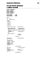
NEW 


REM The NMIL-7040 stepper motor controller can be with the NMIY-0031 

REM processor board to implement a stepper motor control system.  This 

REM program illustrates the commands used to control a stepper in such 

REM a system.  The program uses 0FFE0H as the address of the NMIL-7040. 

REM 


REM Initialize Parameters 

REM No initialization of the NMIL-7040 is needed.  In an actual system, 

REM it may be desirable to position the motor to an initial starting 

REM position. 


10 DUMMY   = 17  : REM Used by delay loop 

20 DELAY   =  4  : REM Number of times through delay loop 

30 MNUMBER =  1  : REM Motor number 

40 DIRECT  =  1  : REM Motor direction 

50 STEEPS  = 10  : REM Number of steps to make in one move 

60 BASEADR = 0FFE0H : REM Base address of NMIL-7040 


100 PRINT " 0   Enter a motor to control (1-4, default = 1)" 

110 PRINT " 1   Change motor direction (default = CW)" 

120 PRINT " 2   Enter the number of steps to move" 

130 PRINT " 3   Issue motor command" 

140 PRINT " 4   Put motor in search mode (does not return to menu)" 

150 INPUT " Enter the number of your selection:  ", CHOICE 

160 ON (CHOICE) GOTO 200, 210, 220, 300, 500 


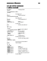
REM Get motor number and check range 

200 INPUT "Enter a motor number (1, 2, 3, 4) to control:  ", MNUMBER 

205 IF ((MNUMBER < 1) .OR. (MNUMBER > 4)) THEN MNUMBER = 1 ELSE GOTO 100 


REM Flip direction bit 

210 DIRECT = DIRECT .XOR. 1 : GOTO 100 


REM Get number of steps and check range 

220 INPUT "Enter the number (positive integer) of steps to make:  ", STEEPS 

225 IF (STEEPS < 1) THEN STEEPS = 10 ELSE GOTO 100 


REM Lines 300 to 350 use MNUMBER (motor number) and REGMASK 

REM to generate the output data for controlling the selected motor. 

REM DIRECT is used to set the direction of motor rotation. 

300 REGMASK = 2 

310 IF (MNUMBER = 1) THEN GOTO 350 

320 FOR I = 2 TO MNUMBER 

330   REGMASK = REGMASK * 4 

340 NEXT I 

350 COMMND = R ((REGMASK/2)*DIRECT) 

REM Lines 360 to 420 then toggle the step line for the selected motor 

REM the requested number of times.  Lines 1070 and 1090 are delays. 

360 FOR I = 1 TO STEEPS 

370   XBY(BASEADR) = COMMND 

380   FOR J = 1 TO DELAY : NEXT J 

390   XBY(BASEADR) = COMMND .XOR. REGMASK 

400   FOR J = 1 TO DELAY : NEXT J 

410 NEXT I 

420 IF (CHOICE = 4) THEN GOTO 510 ELSE GOTO 100 


REM Setup for nearly 1 revolution with fast response, then loop forever 

500 STEEPS = 200 : DELAY = 3 

510 DIRECT = DIRECT .XOR. 01H 

520 GOTO 300 


Summary of Contents for NMIY-0031

Page 1: ...2 2 6 2 0 0 2 2 0 6 P M 1 NMIY 0031 Single Board Computer Covers NMIY 0031 V1 0 4 22 96 ...

Page 2: ...2 2 6 2 0 0 2 2 0 6 P M 2 ...

Page 3: ... O CONNECTORS 19 POWER J12 19 KEYPAD J3 19 LCD J6 20 RS232 J10 20 OPTIONAL CONNECTORS 21 RS422 485 J11 21 VERTICAL STACKING CONNECTORS J1 J7 J9 21 LATCHED and NON LATCHED I O J4 and J5 22 JUMPERS 23 MEMORY CONFIGURATION JUMPERS 23 RESET 24 LCD CONTRAST 25 VERTICAL STACKING COMPONENT VSC CONFIGURATION JUMPERS 25 SERIAL COMMUNICATIONS CONFIGURATION JUMPERS 26 TROUBLESHOOTING 27 MOUNTING 27 POWER SUP...

Page 4: ... MEMORY 33 DATA PORTS 35 KEYPAD I F 35 LCD I F 36 SERIAL I O 38 PROGRAM SEGMENTS 39 MONITOR 39 BASIC 41 C 43 FORTH 46 PART IV 49 DRAWINGS 49 PARTS LIST 51 SILK SCREEN 53 MECHANICAL DRAWING 55 SCHEMATIC 57 57 APPENDICES 59 APPENDIX A 61 APPENDIX B 101 APPENDIX C 147 ...

Page 5: ...ities that promote application development the installed headers option allow flexibility in configuring memory Three languages for development as well as a monitor are also available Other options include an on board power supply up to a 64K program EPROM up to two 32K data ram chips and three COM port standards Customized circuitry can be added in the prototyping area Vertical Stacking Component...

Page 6: ...2 2 6 2 0 0 2 2 0 6 P M 6 ...

Page 7: ...ish chapter titles at the beginning of each section FORTH indicates the formal name of a language or a title reference to another manual chapter or chapter subsection title Enter highlighting signifies a key name for function keys In a program dialog highlighting indicates a user keyed data entry OK indicates a response from software or operating system Bold text is used occasionally where text re...

Page 8: ...2 2 6 2 0 0 2 2 0 6 P M 8 ...

Page 9: ...hased separately from the supplier The RS 232 serial connections are present at J10 Pin J10 3 is data out and pin J10 5 is data in to the 0031 board See the section on I O Connectors for additional detail on J10 connections Once power and terminal connections are established the operating system or monitor EPROM in U2 can be used to work with basic board functions such as the LCD or keypad interfa...

Page 10: ...e system to start up and display the message NMI 8051 MONITOR V1 10 TYPE H FOR HELP _ Please note that the monitor commands must be upper case We strongly recommend that the user put the keyboard in CAPS LOCK mode when using the monitor When the user enters H no enter needed the following help menu appears on the terminal H H help R addr read internal data memory D addr read external data memory P...

Page 11: ...ax FORTH V1 0 This message should appear any time the card is reset including power on The card should be connected through J10 to a terminal or emulator at 9600 baud 8 N 1 With the prototype area of the board to your left looking at the component side of the card J10 is in the upper right hand corner of the board Also J10 Pin1 will be toward the right edge of the card away from the processor U1 a...

Page 12: ...__ 13C8 13BE 1A0C HEX 1A03 DEC____ 13A6 CO__ 139E BU____ 138E DOE__ 135E 1381 1D7A FIL_ 1D72 ERA__ 1D6A BLA__ 1BC1 HOL_ 1892 WOR_ 19C3 CON____ 196D NUM __ 132D FIN_ 124F ID 1012 CRE___ 123F CO______ 121B LIT____ EE4 INT______ 117C IM_______ FE0 VO_________ 1172 FO___ 116A ED____ 1162 AS_______ 1158 RE_____1150 RE______ 153C M___ 1650 M___ 152E R______ 1524 R_______ FD0 CA__ 1315 1315 3E1 LFA 3D8 B...

Page 13: ...31 their locations on the board and basic use Available options also are described I O Connectors gives I O connector locations and pinouts Jumpers describes the location and use of the NMIY 0031 configuration jumpers The Troubleshooting guide has suggestions for items to check if difficulty is encountered getting your board to boot and run These items are ordered in a reasonable sequence for typi...

Page 14: ...2 2 6 2 0 0 2 2 0 6 P M 1 4 ...

Page 15: ...also supported on board The standard NMIY 0031 is a low cost version intended for volume product manufacturing For a development system desirable options include on board power supply expanded memory a development language RS 422 or RS 485 support if needed and headers Other options include EPROM based monitor BASIC FORTH PC based C cross compiler and three interface connectors for Vertical Stacki...

Page 16: ...Interrupt Structure with 2 Priority Levels On Chip Clock Oscillator 64K Program and Data Memory Address Spaces Full Duplex UART Most instructions execute in 1 uS The 8031 uses three control lines for reads and writes PSEN is used for all program instruction fetches Data memory reads and writes use RD and WD These signals provide separate program and data spaces as shown in 8031 8051 manufacturer s...

Page 17: ...pports the data I O latches U5 and U6 and LCD control U10 controls chip select for memory and U9 and memory disable for VSC connectors J1 J7 and J9 See the memory map description in the section Programming for addressing details I O INTERFACES PARALLEL I O Memory mapped and non memory mapped parallel I O are both available on the NMIY 0031 J5 provides direct access to Port 1 of the processor while...

Page 18: ...dent on hardware installed RS232 signals are on J10 while RS422 485 signals are on J11 A MAX232CWE U11 interfaces to RS232C level data lines S1 and S2 provide two additional RS232C control lines J10 and J11 are located near the power connectors along the edge of the board The S1 and S2 headers are located between U11 and U12 13 PROTOTYPING AREA One third of the board area is available for user app...

Page 19: ...for the positive lead and the other terminal nearest to the reset jumper is ground When connecting power be certain you use correct polarity KEYPAD J3 J3 is the keypad connector J3 is located between U1 and J4 near the user component area Pin 1 is located nearest the edge of the board J3 is designed to support a 4 x 5 matrix type keypad Pin connections are Pin Signal Keypad Name 1 PB 0 Y1 2 PB 1 Y...

Page 20: ... closest to the board edge Pin connections are Pin Signal Pin Signal Pin Signal 1 GND 2 5 VDC 3 GND 4 contrast 5 A0 6 contrast 7 WR1 8 E1 9 WR1 10 D0 11 D1 12 D0 13 D2 14 D3 15 D2 16 D4 17 D5 18 D4 19 D6 20 D7 21 D6 22 N C 23 E3 24 N C RS232 J10 J10 is the RS232 connector J10 is located on the edge of the board near R4 the pot and U11 the 232 chip J10 has 10 pins in a dual row header configuration...

Page 21: ...extension to add on cards that mate with the NMIY 0031 A list of currently available VSC card types is in the section Circuit Description J1 is located next to U4 J7 is located next to the prototype area and near U2 and J9 is located between U2 and U3 Each pin 1 is near the long edge of the board and toward the short edge of the board at J1 J1 J7 and J9 each uses a 34 pin dual row header J1 J7 and...

Page 22: ...h the processor I O line requirements J4 lines are latched by U5 and U6 J4 and J5 are located between U1 and the prototype area Pin is in the direction of U1 and closest to U2 J4 CONNECTIONS LATCHED Pin Signal Pin Signal 1 5 V 2 5 V 3 PA 0 4 PA 1 5 PA 2 6 PA 3 7 PA 4 8 PA 5 9 PA 6 10 PA 7 11 GND 12 GND 13 PB 0 14 PB 1 15 PB 2 16 PB 3 17 PB 4 18 PB 5 19 PB 6 20 PB 7 J5 CONNECTIONS NON LATCHED Pin S...

Page 23: ...tra pair of jumper pins to manage both EPROMs and RAM Standard settings configure all locations for an 8K x 8 memory device Alternative settings accommodate 64K x 8 U2 Configuration Jumpers only 32K x 8 and 16K x 8 devices MEMORY CONFIGURATION JUMPERS Location below each memory socket U2 U3 and U4 jumpers N O and P respectively 2764 2864 6264 N U2 8K x 8 O U3 P U4 8K x8 to Pin 1 to Pin 26 to Pin 2...

Page 24: ... 27512 EPROM N U2 64K x 8 to Pin 1 to Pin 26 to Pin 27 x x x x x x H10 H11 and H12 configure U2 U3 and U4 respectively to allow RAM to emulate EPROM by tying the WR pin to VCC To write protect RAM we recommend removal of the corresponding jumper for pin 27 and installing a 100K resistor across the pins of H10 H11 or H12 With battery backup in use RAM emulates ROM RESET Header Q Located near J1 and...

Page 25: ...ted between the power supply section and U9 10 H2 H3 and H4 configure memory locations U2 and U3 H2 selects data only 2 3 or code data 1 2 for U3 H3 selects code data 2 3 or code only 1 2 for U2 Lastly H4 selects 32K 1 2 or 64K 2 3 for U2 H4 H4 U2 32K U2 64K 1 x 2 x x 3 x VERTICAL STACKING COMPONENT VSC CONFIGURATION JUMPERS H5 selects an OE for the VSC connector J1 from either U2 or U3 See figure...

Page 26: ... format will be used for communications H8 selects between RS232 format and RS422 485 H7 and H9 select between RS422 and RS485 Standard configuration uses RS232 Optional components must be installed for either RS422 or RS485 H6 H6 H8 H8 int 0 int 1 RS232 RS422 RS485 1 x x 2 x x x x 3 x x H7 H7 H9 H9 RS422 RS485 RS422 RS485 1 x x 2 x x x x 3 x x ...

Page 27: ...uire 6 3 to 10 VAC alternatively 9 to 14 VDC at connector J2 Check for correct power in either version with a meter or scope at the screw terminals of J12 When the supply is correct there will be 5 VDC 5 with less than 80 mV ripple in either version at J12 Use of an oscilloscope is recommended whenever there is a question concerning power supply regulation OPERATING SYSTEM Every CPU requires a bas...

Page 28: ...that your cable supports these lines if required See the I O Connector section to check your cable pinout Remember to align pin 1 of J10 and your cable Pin 1 is the J10 pin closest to the corner of the board KEYPAD and LCD I O Keypad input requires program support Keypad and LCD connectors are J3 and J6 respectively NMIY 0031 hardware supplies the necessary hardware control and data lines to make ...

Page 29: ... inches VSC MOUNTING The NMIY 0031 has connector pads for three VSC connectors When these optional connectors are installed there are three sites for adding VSC cards A VSC card plugs into the NMIY 0031 from above the component side of the board The mounting holes for VSC cards are located in ears along both long sides of the NMIY 0031 board The projecting mounting ears each extend 3 8 inch from t...

Page 30: ...2 2 6 2 0 0 2 2 0 6 P M 2 2 6 2 0 0 2 3 0 ...

Page 31: ...ing the NMIY 0031 Programming gives information on program and data address spaces and programming locations and commands for hardware resources Program Segments provides sample program segments to illustrate use of commands to hardware resources such as the keypad port and LCD interface Program segments are provided for Monitor BASIC C and FORTH ...

Page 32: ...2 2 6 2 0 0 2 2 0 6 P M 2 2 6 2 0 0 2 3 2 ...

Page 33: ...al logic An additional port latched with eight inputs and eight outputs is available at J4 MEMORY Three memory sockets are provided on the NMIY 0031 U2 is intended for the operating system Available items for U2 are BASIC FORTH and Monitor A Small C compiler is also available on diskette Using C the user can install an EPROM with a custom application operating system for production To support rapi...

Page 34: ...U4 is 0000 Up to a 32Kx8 RAM may be used in U4 A 32Kx8 RAM installed in U4 is addressed from 0000 to 7FFF as data ADDRESS SPACES U2 U3 U4 Program Data Program Data Program Data NNNN NNNN FFFF NNNN NNNN NNNN NNNN NNNN NNNN NNNN NNNN FC00 NNNN NNNN SSSAA NNNN SSSSSS SSSAA NNNN NNNN SSSAA NNNN SSSSSS SSSAA NNNN NNNN SSSAA NNNN SSSSSS SSSAA NNNN NNNN SSSAA NNNN 7FFF SSSSSS SSSAA NNNN NNNN AAAA NNNN NN...

Page 35: ...e used to signal when particular services are needed from the processor The timer outputs counter inputs are useful for checking time dependent processes Also the direct data inputs are useful for bit oriented input output These are a few suggestions for using the direct input output connections See an 8031 51A data book for details on timer counter and interrupt programming KEYPAD I F The NMIY 00...

Page 36: ...to the original position Data storage is unchanged Entry Mode Set is a group of related commands This group determines the cursor move direction and specifies whether to shift the display Each of these commands sets the mode used when writing data to the LCD 04 Move cursor to left Do not shift the display 06 Move the cursor to the right Do not shift the display normal 05 Move the cursor to the lef...

Page 37: ...rs on each line while displaying only a contiguous segment of that line equal to the number of display characters The position addresses are shown above where the 16 20 and 40 character display line end addresses are noted Note that these address limits assume that the first character displayed is the first character of that line in memory Using the shift feature the first character displayed can ...

Page 38: ...troller addresses are FFFA for commands and FFFB for data SERIAL I O Serial I O is available through the 8031 processor s serial port For most users the I O routines built into BASIC FORTH and C will support use of this port See an 8031 51A data book for details on assembly language usage Serial interface electrical format is determined by which chips among U11 U12 and U13 are installed and the se...

Page 39: ... allowed and included for readability The comments on each line are rejected by the monitor and should not be entered O 38 FFF8 Set 2 line display and 5x7 dot format O 38 FFF8 Set 2 line display and 5x7 dot format O 06 FFF8 Entry mode cursor moves to right no display shift O 0F FFF8 Set display and blinking cursor on O 01 FFF8 Clear Display O 80 FFF8 Set cursor to left end of line one O 22 FFF9 Di...

Page 40: ...w 4 returns F7 The value returned by any other column will be FF E X AM P L E If the key in row 3 column 2 is pressed then after entering O FD FFFC D FFFC FB the value FB is returned while all other columns will return FF The FB hex return value signifies a row 2 key is pressed Bit 2 of FB has a zero value which identifies the row as 3 Remember to hold the key pad key down while entering the D com...

Page 41: ...ed The specific coordinates are then determined and written to the next line on the LCD The keypad scan is then resumed until another key is pressed NEW 10 STRING 22 20 REM Allocate string space 20 I 0 22 ROW 0 REM Initialize row and column indices 24 COL 0 REM Constants 30 KEYPAD 0FFFCH REM Keypad latch write read address 32 LCDCMD 0FFF8H REM Display command address 34 LCDDAT 0FFF9H REM Display d...

Page 42: ...IALIZATION INSTRUCTIONS REM Initialize Array 1100 B 1 0FEH REM Initialize column address vector 1110 B 2 0FDH 1120 B 3 0FBH 1130 B 4 0F7H 1140 B 5 0EFH REM Initialize Display 1200 XBY LCDCMD 038H REM Get attention 1210 XBY LCDCMD 038H REM Set 2 line display and 5x7 dot format 1220 XBY LCDCMD 006H REM Entry mode cursor to right no shift 1230 XBY LCDCMD 00FH REM Set display and blinking cursor on 12...

Page 43: ...de clib alloc c include clib peekpoke c include clib getchar c include clib fgetc c main char ch1 int coldata row col _lcdinit _lcdbusy while EOF coldata 1 col 0 row 0 for col 1 col 6 col scan columns _kpad_put coldata 0xFF output column bit if row _kpad_get ch1 check for key press while row _kpad_get ch1 de bounce key press _lcdhome _dispdata row col display key press else coldata coldata 1 end f...

Page 44: ...eekb adr 0x00FF return ch _lcdbusy wait for LCD not busy int adr adr 0x0FFF8 while peekb adr 0x0080 _lcdput ch write display data to LCD char ch int adr adr 0x0FFF9 _lcdbusy wait pokeb adr ch send character _lcdcr set LCD cursor to other line char z int i adr _lcdbusy compute other line address adr 0xFFF8 z peekb adr 0x0040 0x00C0 pokeb adr z set cursor at BOL for i 0 i i 40 clear to LCD EOL _lcdp...

Page 45: ...FFF8 _lcdbusy pokeb adr 0x0001 _lcdinit reset LCD display int adr adr 0xFFF8 _lcdbusy wait pokeb adr 0x0038 get attention _lcdbusy pokeb adr 0x0038 8 bit data 2 lines 5x7 dots _lcdbusy pokeb adr 0x0006 cursor inc no display shift _lcdbusy pokeb adr 0x000F display on blinking cursor on _lcdbusy pokeb adr 0x0001 clear display set cursor to home ...

Page 46: ...ISPLAY DSP AT n DUP DC L MOD 080 OR SWAP DC L 1 IF 040 OR THEN WAIT NOT BUSY DSP CMD C return cursor position C URSOR n WAIT NOT BUSY DSP CMD C 07F AND print a character move cursor to left DSP EMIT char WAIT NOT BUSY DSP DATA C print a string on the LCD writes past end of line DSP TYPE addr n DUP IF 0 DO COUNT DSP EMIT LOOP THEN DROP init the display DSP ON WAIT NOT BUSY 038 DSP CMD C get attenti...

Page 47: ...PAD n KPAD C detect keypress KPAD row 0 KPAD BEGIN KPAD UNTIL KPAD determine which row and column are pressed values are saved in variables ROW and COL SCAN 0FFFF ROW 0FFFF COL TOT COL 0 DO I 2 0FF XOR KPAD TOT ROW 0 DO KPAD I 2 AND IF I ROW J COL THEN LOOP LOOP CONVERT KPAD ROW COL n map key coordinates to single ASCII character ROW TOT COL COL DUP 04 IF DROP 017 ELSE convert unlabeled keys DUP 0...

Page 48: ...ess KPAD PRESS BEGIN SCAN COL ROW AND 0FFFF NOT UNTIL de bounce key pad KPAD RELEASE COL 2 0FF XOR KPAD BEGIN KPAD ROW 2 AND 0 UNTIL get and de bounce key press GET KPAD KPAD PRESS CONVERT KPAD KPAD RELEASE get key press and display on LCD KPAD DSP DSP ON BEGIN GET KPAD DSP EMIT TERMINAL UNTIL DECIMAL ...

Page 49: ... 0 2 2 0 6 P M 2 2 6 2 0 0 2 4 9 N M I Y 0 0 3 1 P A R T I V D R A W I N G S PART IV DRAWINGS The Drawings section contains the parts list silk screen for the board mechanical detail drawing and board schematic ...

Page 50: ...2 2 6 2 0 0 2 2 0 6 P M 2 2 6 2 0 0 2 5 0 ...

Page 51: ...Y 0031 BOARD Connector 34 pin VSC J1 Resistor 1K 5 W R8 dual row header Resistor 4 7K 5 W R2 3 Spacer 34 pin VSC Resistor 10K 5 W R5 7 9 Diode 1N4148 D1 3 Resistor 10K 10P9E RN1 Bridge rectifier DB101 CR1 Resistor 10K pot R4 Regulator 7805 VR1 Resistor 10M 5 W R1 IC GAL16V8 U9 10 Socket 8 pin U12 13 IC MAX232 U11 Socket 16 pin U11 IC 8K BASIC EPROM U2 Socket 20 pin U5 6 8 9 10 IC 8K MONITOR U2 Soc...

Page 52: ...2 2 6 2 0 0 2 2 0 6 P M 2 2 6 2 0 0 2 5 2 ...

Page 53: ...H 7 H 8 1 R4 C 1 U 5 74HC245 J H1 1 J 5 P B G N G N G N G N G N G N G N G N G N 4 2 2 X 4 2 2 R P B P 1 P 1 P 1 P B D D P A D P 1 P 1 D P A C S P 1 I N T P B R S S O T P A E P 1 P A 5 5 5 5 5 I N T S I D A C W R E A C A T P 1 D D V O D N M I Y 0 0 3 18 0 5 1 1 6 0 1C H A L K D A L L A S T X 2 1 4 3 3 9 N E WM I C R O S N J 5 R S 5 P 1 P 1 P 1 P 1 G N 5 I N T T T O I N T 5 G N P 1 P 1 P 1 P 1 5 G N...

Page 54: ...2 2 6 2 0 0 2 2 0 6 P M 2 2 6 2 0 0 2 5 4 ...

Page 55: ...7517 74ΗΧ5 74ΗΧ2 ϑ 0 000 0 187 0 200 0 250 2 325 2 628 3 200 3 575 4 125 4 275 4 300 4 563 4 750 17 0 110 12 0 156 0 150 0 200 0 250 0 450 1 100 1 750 1 925 2 175 2 350 3 700 3 800 3 850 4 025 4 275 6 125 6 200 6 300 4 145 4 125 2 975 1 975 0 725 0 625 0 604 6 012 6 300 6 200 5 950 4 450 4 400 3 850 3 800 3 650 3 200 2 350 2 300 1 850 1 050 1 750 0 250 0 200 0 150 0 000 ...

Page 56: ...2 2 6 2 0 0 2 2 0 6 P M 2 2 6 2 0 0 2 5 6 ...

Page 57: ...19 1 11 3 4 7 8 13 14 17 18 RO DI RE DE B A U13 12 3 4 6 7 H9 1 2 3 J10 1 2 3 4 5 6 7 8 9 10 H12 1 2 CS D7 D6 D5 D4 D3 GND D2 D1 D0 A0 A1 A2 A3 A4 A5 A6 A7 A12 5A8 A9 A11 A10 OE MEMORY U4 1 2 3 4 5 6 7 8 9 10 11 12 13 14 15 16 17 18 19 20 21 22 23 24 25 26 27 28 D2 1 2 1N4148 J12 12 J3 1 2 3 4 5 6 7 8 9 RN1 1 4 RN1 1 9 RN1 1 7 RN1 1 2 VCC I O7 I O6 I O5 I O4 I O3 I O2 I O1 I O0 G OE GND I8 I7 I6 I...

Page 58: ...2 2 6 2 0 0 2 2 0 6 P M 2 2 6 2 0 0 2 5 8 ...

Page 59: ...ystem may be added to a stack as needed until bus loading becomes an issue Sample code is included in BASIC C and FORTH for LCD and Keypad interfaces on NMIY 0031 NMIL 1055 24 BIT I O board NMIL 3003 64 Input HC compatible board NMIL 3004 64 Output HC compatible board NMIL 4000 8 Channel 8 Bit Digital to Analog board NMIL 4004 1 Channel 12 Bit Analog to Digital board NMIL 5000 ACIA 1 Channel Seria...

Page 60: ...2 2 6 2 0 0 2 2 0 6 P M 2 2 6 2 0 0 2 6 0 ...

Page 61: ...ample program for each of the listed NMIL cards Sample programs show the requirements for using the boards Fundamental communications routines are given and typically brought together with a user interface Many of the routines are coded to stress clarity in reading rather than efficiency relative to BASIC ...

Page 62: ...2 2 6 2 0 0 2 2 0 6 P M 2 2 6 2 0 0 2 6 2 ...

Page 63: ...ow 3 as row 2 REM Similarly for the columns NEW 10 STRING 22 20 REM Allocate string space 20 I 0 22 ROW 0 REM Initialize row and column indices 24 COL 0 REM Constants 30 KEYPAD 0FFFCH REM Keypad latch write read address 32 LCDCMD 0FFF8H REM Display command address 34 LCDDAT 0FFF9H REM Display data address 35 LCDLINE 20 REM Display line length 36 NUMROWS 4 REM Number of display rows 37 NUMCOLS 5 RE...

Page 64: ...NSTRUCTIONS REM Initialize Array 1100 B 1 0FEH REM Initialize column address vector 1110 B 2 0FDH 1120 B 3 0FBH 1130 B 4 0F7H 1140 B 5 0EFH REM Initialize Display 1200 XBY LCDCMD 038H REM Get attention 1210 XBY LCDCMD 038H REM Set 2 line display and 5x7 dot format 1220 XBY LCDCMD 006H REM Entry mode cursor to right no shift 1230 XBY LCDCMD 00FH REM Set display and blinking cursor on 1240 XBY LCDCM...

Page 65: ...CNTROL 01H 1130 PRINT Is Port C BITS 4 7 input or output 1140 PRINT Enter a 1 for input or a 0 for output 1150 INPUT PCHVALUE PRINT 1160 IF PCHVALUE 0 THEN CNTROL CNTROL 08H 1170 XBY 0FFE3H CNTROL REM Get and set port output values 1200 GOSUB 10700 REM Get value and output to Port A 1210 IF PBVALUE THEN GOTO 1230 1220 GOSUB 10800 REM Get value and output to Port B 1230 IF PCHVALUE OR PCLVALUE THEN...

Page 66: ...NT Enter value to output to Port A 10710 INPUT PORTA 10720 XBY 0FFE0H PORTA 10730 RETURN REM Get value and output to Port B 10800 PRINT Enter value to output to Port B 10810 INPUT PORTB 10820 XBY 0FFE1H PORTB 10830 RETURN REM Get value and output to Port C 10900 PRINT Enter value to output to Port C 10910 INPUT PORTC 10920 XBY 0FFE2H PORTC 10930 RETURN ...

Page 67: ...ements REM REM The NMIL 3003 is a 64 input HC compatible board This sample REM program segment will read the ports consecutively and display REM the values read across the screen REM REM First read all ports REM 1000 PORTA XBY 0FFE0H 1010 PORTB XBY 0FFE1H 1020 PORTC XBY 0FFE2H 1030 PORTD XBY 0FFE3H 1040 PORTE XBY 0FFE4H 1050 PORTF1 XBY 0FFE5H 1060 PORTG XBY 0FFE6H 1070 PORTH XBY 0FFE7H REM Now dis...

Page 68: ...2 2 6 2 0 0 2 2 0 6 P M 2 2 6 2 0 0 2 6 8 ...

Page 69: ...t A PORTA 1010 INPUT Enter a value to write to port B PORTB 1020 INPUT Enter a value to write to port C PORTC 1030 INPUT Enter a value to write to port D PORTD 1040 INPUT Enter a value to write to port E PORTE 1050 INPUT Enter a value to write to port F PORTF1 1060 INPUT Enter a value to write to port G PORTG 1070 INPUT Enter a value to write to port H PORTH REM Write all ports REM 1100 XBY 0FFE0H...

Page 70: ...2 2 6 2 0 0 2 2 0 6 P M 2 2 6 2 0 0 2 7 0 ...

Page 71: ...down the changes to fast meter response time REM 100 FOR I 1 TO 255 STEP 39 REM 130 FOR K 1 TO 1000 NEXT K 180 NEXT OUTVAL 200 GOTO 100 REM Initialize DAC channel address pointers and outputs 10000 CH 1 BASEADDRESS 0 10010 CH 2 BASEADDRESS 1 10020 CH 3 BASEADDRESS 2 10030 CH 4 BASEADDRESS 3 10040 CH 5 BASEADDRESS 4 10050 CH 6 BASEADDRESS 5 10060 CH 7 BASEADDRESS 6 10070 CH 8 BASEADDRESS 7 REM Init...

Page 72: ...2 2 6 2 0 0 2 2 0 6 P M 2 2 6 2 0 0 2 7 2 ...

Page 73: ...0 ON CHOICE GOSUB 11500 11000 10100 10200 10240 1095 GOTO 1000 REM Set channel start conversion wait then read 10000 XBY BASEADR CHNUM 10010 XBY BASEPL1 0 10020 FOR I 0 TO DELAY NEXT I 10030 RDVALUE XBY BASEPL2 010H XBY BASEPL3 010H 10099 RETURN REM Scan outputs scales by 1 and prints to screen in a loop 10100 GOSUB 10800 REM Make title 10110 DO 10120 GOSUB 10300 REM Unitary scale and display 1013...

Page 74: ...R J 0 TO 7 10610 CHNUM J 10620 GOSUB 10000 REM read channel 10630 GOSUB 10500 REM Scale for 20V input 10640 PRINT RDVALUE 10660 NEXT J 10670 PRINT 10679 RETURN REM Make title 10800 FOR I 1 TO 26 PRINT NEXT I 10810 PRINT Channel Readings PRINT 10820 PRINT 0 1 2 3 4 5 6 7 10830 PRINT 10899 RETURN REM Routine to test and report all channels 11000 PRINT 11010 DO 11020 FOR J 0 TO 7 11030 CHNUM J 11040 ...

Page 75: ...e start 8 bit conversion 13120 XBY BASEPL3 0FFH 13129 RETURN REM Read 8 bit 13130 RDVAL XBY BASEPL2 13139 RETURN REM Start 12 bit conversion 13140 XBY BASEPL2 0 13149 RETURN REM Alternate start 12 bit conversion 13150 XBY BASEPL2 0FFH 13159 RETURN REM Read 12 bit 13160 RDVAL XBY BASEPL2 RDVAL2 XBY BASEPL3 13169 RETURN REM Scale 12 bit reading 13170 RDVAL RDVAL 10 AND 0FFFH 13179 RETURN ...

Page 76: ...2 2 6 2 0 0 2 2 0 6 P M 2 2 6 2 0 0 2 7 6 ...

Page 77: ... 15 19200 26 BAADS 16 38400 REM Initialize NMIL 5000 110 CMMAND 0CBH 120 CNTROL 01CH 130 GOSUB 10000 REM Initialize registers REM Main control loop menu 1000 1010 0 Report status register 1020 1 Report command register 1030 2 Report control register 1040 3 Send a test pattern to remote 1050 4 Receive test1 1060 5 Receive test w RTS handshaking for RS232 1070 6 Test full duplex 1080 7 Receive test ...

Page 78: ...H THEN PRINT Transmitter empty 20150 IF STATUS AND 8H THEN PRINT Receiver data register full 20160 IF STATUS AND 4H THEN PRINT Overrun has occurred 20170 IF STATUS AND 2H THEN PRINT Framing error detected 20180 IF STATUS AND 1H THEN PRINT Parity error detected 20185 IF STATUS 010H THEN PRINT Status is waiting for data 20190 RETURN REM Parity type report 20200 CMMANDN CMMAND 20210 IF CMMANDN AND 20...

Page 79: ... 20700 CNTROL XBY 0FFE3H AND 0E0H 20702 IF CNTROL AND 060H 0H THEN PRINT 8 bits 20704 IF CNTROL AND 060H 020H THEN PRINT 7 bits 20706 IF CNTROL AND 060H 040H THEN PRINT 6 bits 20708 IF CNTROL AND 060H 060H THEN PRINT 5 bits 20710 IF CNTROL 080H THEN PRINT 1 stop bit GOTO 20790 REM Get Receiver Echo Mode 20720 CMMAND XBY 0FFE2H AND 020H REM Get WL1 and WL0 20730 CNTROL CNTROL AND 60H 20740 IF CNTRO...

Page 80: ...nitialize 30100 GOSUB 9999 REM Initialize board 30110 RDSTATUS 0 30112 NUCHAR 0 30120 DO REM Get next character 30130 GOSUB 10400 REM Get next character 30140 PRINT CHR NEXIN REM Exit on control C 30150 UNTIL NEXIN 3 30160 NEXIN 0 30190 RETURN REM Receive test with RTS handshaking for RS232 REM Initialize 30200 GOSUB 9999 REM Initialize board 30210 RDSTATUS 0 30212 NUCHAR 0 30220 DO 30230 XBY 0FFE...

Page 81: ...e status 30350 IF RDSTATUS THEN NEXIN XBY 0FFE0H CHR NEXIN RDSTATUS 0 30360 NEXOUT I 30370 GOSUB 10300 REM Send next character REM Delay for slow remote 30380 NEXT I 30390 UNTIL NEXIN 03H 30392 NEXIN 0 30399 RETURN REM Test receive with no RTS handshaking REM Initialize 30400 CMMAND 0D3H 30402 CNTROL 01CH 30404 GOSUB 10000 REM Initialize comm parameters 30410 RDSTATUS 0 30420 DO 30430 GOSUB 10400 ...

Page 82: ...2 2 6 2 0 0 2 2 0 6 P M 2 2 6 2 0 0 2 8 2 ...

Page 83: ...M communications program such as MAX TERM The user is queried for REM values to use in setting the outputs of the NMIL 7001 REM REM Port A is addressed at 0FFE0H and REM Port B is addressed at 0FFE1H REM 1000 PRINT NMIL 7001 outputs are inverted Setting a bit to 1 1010 PRINT turns the output off setting a bit to 0 turns the 1020 PRINT corresponding output on PRINT 1030 INPUT Please enter a value f...

Page 84: ...2 2 6 2 0 0 2 2 0 6 P M 2 2 6 2 0 0 2 8 4 ...

Page 85: ...ser REM is queried for values to use in setting the outputs of the REM NMIL 7003 the values are then output and the inputs are read and REM displayed through COM1 REM REM The user is queried for a value to output to port B The value is REM then sent to port B and the value of port A is read and displayed REM The sequence is then repeated until run is terminated REM REM Port A is addressed at 0FFE0...

Page 86: ...2 2 6 2 0 0 2 2 0 6 P M 2 2 6 2 0 0 2 8 6 ...

Page 87: ...ay number to turn on RELAYNUM 1110 IF RELAYNUM 0 THEN GOTO 1180 1120 IF RELAYNUM 1 THEN RELAYNUM 1 1130 IF RELAYNUM 8 THEN RELAYNUM 8 1140 MASK 1 RELAYNUM RELAYNUM 1 1150 IF RELAYNUM 0 THEN FOR I 1 TO RELAYNUM MASK MASK 2 NEXT I 1160 COPYR COPYR OR MASK 1170 XBY PORTADR COPYR 1180 GOTO 1000 REM Get a relay to turn off and turn it off 1200 INPUT Please enter a relay number to turn off RELAYNUM 1210...

Page 88: ...2 2 6 2 0 0 2 2 0 6 P M 2 2 6 2 0 0 2 8 8 ...

Page 89: ...de does not return to menu 150 INPUT Enter the number of your selection CHOICE 160 ON CHOICE GOTO 200 210 220 300 500 REM Get motor number and check range 200 INPUT Enter a motor number 1 2 3 4 to control MNUMBER 205 IF MNUMBER 1 OR MNUMBER 4 THEN MNUMBER 1 ELSE GOTO 100 REM Flip direction bit 210 DIRECT DIRECT XOR 1 GOTO 100 REM Get number of steps and check range 220 INPUT Enter the number posit...

Page 90: ...2 2 6 2 0 0 2 2 0 6 P M 2 2 6 2 0 0 2 9 0 ...

Page 91: ...sheets for additional detail REM REM Initialize NMIL 7056 REM Software reset 10 CLEAR 15 STRING 10 8 20 CMDADR 0FFE0H 25 DAT1ADR 0FFE1H 30 GOTO 10500 REM Initialize system REM Main User Loop 100 REM FOR I 1 TO 26 PRINT NEXT I 105 PRINT 0 Absolute Move requires a numerical position input 110 PRINT 1 Load Trajectory 115 PRINT 2 Relative Move requires a numerical offset input 120 PRINT 3 Left Velocit...

Page 92: ...0 Position GOSUB 9000 1135 GOSUB 10005 XBY CMDADR 01FH REM Send Trajectory Control Word 1136 DATBYTE2 000H DATBYTE1 003H GOSUB 10010 REM Send position data 1137 DATBYTE2 I4 DATBYTE1 I3 GOSUB 10010 1138 DATBYTE2 I2 DATBYTE1 I1 GOSUB 10010 REM Load and Start trajectory 1139 GOSUB 10099 GOTO 105 REM Left Velocity Move 1150 0 Velocity GOSUB 9000 1153 GOSUB 10005 XBY CMDADR 01FH REM Send Trajectory Con...

Page 93: ... DATBYTE2 0FFH DATBYTE1 0FFH GOSUB 10010 1206 DATBYTE2 0FDH DATBYTE1 0F8H GOSUB 10010 1209 GOSUB 10099 GOTO 1250 REM Load Filter Parameters 1210 0 Kp GOSUB 9000 KP2 I2 KP1 I1 1220 0 Ki GOSUB 9000 KI2 I2 KI1 I1 1230 0 Kd GOSUB 9000 KD4 I2 KD3 I1 1240 0 Il GOSUB 9000 IL4 I2 IL3 I1 1247 FILTCW1 00FH 1249 GOSUB 10120 GOTO 105 REM Load filter param and issue UDF REM Motor Power OFF REM Load Turn Off Mo...

Page 94: ... 10005 10019 RETURN REM Read double byte and check for cleared busy bit 10020 GOSUB 10005 10022 DATBYTE2 XBY DAT1ADR 10024 GOSUB 10005 10026 DATBYTE1 XBY DAT1ADR 10029 RETURN REM Stop wait for move end 10030 GOSUB 10005 10032 XBY CMDADR 01FH 10035 DATBYTE2 002H 10036 DATBYTE1 000H GOSUB 10010 REM Issue STT to activate motor stop command 10037 GOSUB 10005 10038 XBY CMDADR 001H REM Wait For Move End...

Page 95: ...185 DATBYTE2 VELOCTY2 DATBYTE1 VELOCTY1 GOSUB 10010 10190 DATBYTE2 POSITIN4 DATBYTE1 POSITIN3 GOSUB 10010 10195 DATBYTE2 POSITIN2 DATBYTE1 POSITIN1 GOSUB 10010 REM Issue STT to activate changes 10199 GOTO 10099 REM RDSIGS ReaD SIGnalS Register 10200 GOSUB 10005 XBY CMDADR 00CH GOSUB 10005 10205 RDSIGS2 XBY DAT1ADR GOSUB 10005 10209 RDSIGS1 XBY DAT1ADR GOTO 10005 REM RDIP ReaD Index Position 10220 ...

Page 96: ...tus STATUS 10570 GOSUB 10005 XBY CMDADR 000H REM Parameter Initialization 10590 GOSUB 10005 XBY CMDADR 01CH GOSUB 10005 10600 DATBYTE2 000H DATBYTE1 000H GOSUB 10010 REM Reset interrupts 10610 GOSUB 10001 REM Initialize and Load Filter Parameters 10620 KP2 000H KP1 010H KI2 000H KI1 010H 10630 KD2 000H KD1 00AH IL2 000H IL1 010H 10640 FILTCW2 000H FILTCW1 00FH 10650 GOSUB 10120 REM Load filter par...

Page 97: ...sserted before read or write to clock REM Processor must clear busy bit before proceeding REM HOLD CLOCK REM When not busy set HOLD bit and return REM Set HOLD bit 100 XBY 0FFEDH 1 REM Check BUSY bit 110 T1 XBY 0FFEDH REM Mask off bits 2 7 120 T1 T1 INT T1 4 REM If busy then wait and reassert HOLD else return 130 IF T1 2 THEN RETURN REM Hold is set low for at least 61 uS to clear busy bit 140 XBY ...

Page 98: ...limits then get and write tens and ones values 10000 IF SECND 0 THEN SECND 0 10010 IF SECND 59 THEN SECND 59 10020 TEMP INT SECND 10 10030 SECND SECND TEMP 10 10040 GOSUB 100 XBY 0FFE1H TEMP XBY 0FFEDH 0 10050 GOSUB 100 XBY 0FFE0H SECND XBY 0FFEDH 0 REM SET MINUTE REM Check limits then get and write tens and ones values 10100 IF MINUTE 0 THEN MINUTE 0 10110 IF MINUTE 59 THEN MINUTE 59 10120 TEMP I...

Page 99: ... REM Read and process tens digit first REM Same for each clock segment REM Get tens digit first 12000 GOSUB 100 SECND XBY 0FFE1H XBY 0FFEDH 0 REM Must clear hold bit within 1 sec 12010 GOSUB 100 TEMP XBY 0FFE0H XBY 0FFEDH 0 12020 SECND SECND 10 TEMP REM Read minutes 12100 GOSUB 100 MINUTE XBY 0FFE3H XBY 0FFEDH 0 12110 GOSUB 100 TEMP XBY 0FFE2H XBY 0FFEDH 0 12120 MINUTE MINUTE 10 TEMP REM Read HR24...

Page 100: ...810 IF DW 0 THEN PRINT SUN 12811 IF DW 1 THEN PRINT MON 12812 IF DW 2 THEN PRINT TUE 12813 IF DW 3 THEN PRINT WED 12814 IF DW 4 THEN PRINT THU 12815 IF DW 5 THEN PRINT FRI 12816 IF DW 6 THEN PRINT SAT 12820 PRINT MNTH DAY YEAR HOUR 12830 PRINT MINUTE SECND 12840 IF HR24_12 0 THEN PRINT GOTO 12860 12850 IF AM_PM 0 THEN PRINT PM ELSE PRINT AM 12860 RETURN ...

Page 101: ...gram for each of the listed NMIL cards Sample programs show the communications requirements for using the boards Fundamental communications routines are given and typically brought together with a user interface Many of the routines are coded to stress clarity in reading rather than efficiency relative to C ...

Page 102: ...2 2 6 2 0 0 2 2 0 6 P M 2 2 6 2 0 0 2 1 0 2 ...

Page 103: ...l lcdinit lcdbusy while EOF coldata 1 col 0 row 0 for col 1 col 6 col scan columns kpad_put coldata 0xFF output column bit if row kpad_get ch1 check for key press while row kpad_get ch1 debounce key press lcdhome dispdata row col display key press else coldata coldata 1 end for end while end main dispdata row col output data to lcd int row col if row 0x0004 row 3 else if row 0x0008 row 4 lcdput ro...

Page 104: ...other line address z peekb LCDSTAT 0x0040 0x00C0 pokeb LCDSTAT z set cursor at BOL for i 0 i i 40 clear to LCD EOL lcdput clear next position lcdbusy wait pokeb LCDSTAT z reposition cursor end lcd carriage return write lcdhome set lcd cursor at home position lcdbusy pokeb LCDSTAT 0x0001 end set lcd cursor at home position lcdinit reset lcd display int adr adr 0xFFF8 lcdbusy wait pokeb adr 0x0038 g...

Page 105: ...Y0031 clib ungetc c include c NMIY0031 clib utoi c define portA 0xFFE0 define S 1055 register addresses define portB 0xFFE1 define portC 0xFFE2 define cntl_reg 0xFFE3 int cntrol configuration variables cfiga cfigb cfigcl cfigch porta_in port read variables portb_in portc_in porta_out portb_out portc_out temp This program demonstrates the use of the NMIL 1055 24 bit I O card with the NMIY 0031 proc...

Page 106: ... printf nInput a hex value for port C high bits 4 7 fscanf stdin x temp portc_out portc_out temp 0xF0 end if output_ports end while end main cnfig cntrol 0x80 printf nThe direction of the ports needs to be configured printf nFor ports A B C low and C high nenter a 0 for output or a 1 for input printf nPort A fscanf stdin d cfiga if cfiga 0 cntrol 0x10 printf nPort B fscanf stdin d cfigb if cfigb 0...

Page 107: ...ortB portc_in peekb portC printf n if cfiga 0 printf nPort A input is x n porta_in if cfigb 0 printf Port B input is x n portb_in mask 0 if cfigcl 0 mask 0x0F if cfigch 0 mask 0xF0 if mask 0 printf Port C input is x n n portc_in mask printf n return 0 end input_ports output_ports pokeb portA porta_out pokeb portB portb_out pokeb portC portc_out return 0 end output_ports ...

Page 108: ...2 2 6 2 0 0 2 2 0 6 P M 2 2 6 2 0 0 2 1 0 8 ...

Page 109: ...C 0xFFE2 define PORTD 0xFFE3 define PORTE 0xFFE4 define PORTF 0xFFE5 define PORTG 0xFFE6 define PORTH 0xFFE7 int adata bdata cdata ddata edata fdata gdata hdata temp The NMIL 3003 is a 64 input HC compatible board This sample program demonstrates use of the NMIL 3003 with the NMIY 0031 processor card The ports are read consecutively and then the values read are displayed across the screen After re...

Page 110: ...2 2 6 2 0 0 2 2 0 6 P M 2 2 6 2 0 0 2 1 1 0 ...

Page 111: ...lib ungetc c include c NMIY0031 clib utoi c define PORTA 0xFFE0 define PORTB 0xFFE1 define PORTC 0xFFE2 define PORTD 0xFFE3 define PORTE 0xFFE4 define PORTF 0xFFE5 define PORTG 0xFFE6 define PORTH 0xFFE7 int adata bdata cdata ddata edata fdata gdata hdata temp The NMIL 3004 is a 64 output HC compatible board This sample program segment demonstrates the NMIL 3004 used with the NMIY 0031 processor b...

Page 112: ...ort C scanf x cdata printf nEnter a HEX value for port D scanf x ddata printf nEnter a HEX value for port E scanf x edata printf nEnter a HEX value for port F scanf x fdata printf nEnter a HEX value for port G scanf x gdata printf nEnter a HEX value for port H scanf x hdata end get values write_outputs pokeb PORTA adata pokeb PORTB bdata pokeb PORTC cdata pokeb PORTD ddata pokeb PORTE edata pokeb ...

Page 113: ...ogram will exercise the NMIL 4000 8 channel D A card when used with the NMIY 0031 processor All 8 channels are simultaneously stair stepped through the range of output values A delay for meter testing is included but commented out main int i delay dummy offset while 1 for i 1 i 255 i for offset 0 offset 8 offset pokeb BASEADR offset i Uncomment the following line to read the output with a meter fo...

Page 114: ...2 2 6 2 0 0 2 2 0 6 P M 2 2 6 2 0 0 2 1 1 4 ...

Page 115: ...NELB 0xFFE1 channel number for 8 bit define D_REG 0xFFE2 upper 8 bits of converted value define D_REG_B 0xFFE3 lower 4 bits left justified This program is written to exercise the NMIL 4004 8 channel A D card when used with the NMIY 0031 processor board Routines are provided for calibration test and monitoring of inputs scanning unsigned int channel_num choice read_value scale_factor main choice 0 ...

Page 116: ..._num pokeb D_REG 0 for i 0 i DELAY i dummy i i 0x0D read_value peekb D_REG 0x10 peekb D_REG_B 0x10 return 0 end convert print_title printf n n n n n Channel Number printf n 0 1 2 3 4 5 6 7 end print title Scale to 10V range then keep two decimal places as scaled int The result is then scaled to requested scale x1 x10 or x20 Performing integer operations in this order prevents arithmetic overflow 4...

Page 117: ...I L 4 0 0 4 8 C H A N N E L A D C S A M P L E P R O G R A M tabulate printf n print_title printf n while 1 for channel_num 0 channel_num 8 channel_num convert scale_it printf 4d 2d read_value 100 read_value 100 end for printf n end while end tabulate ...

Page 118: ...2 2 6 2 0 0 2 2 0 6 P M 2 2 6 2 0 0 2 1 1 8 ...

Page 119: ...EG 0xFFE0 define STATUS_REG 0xFFE1 define COMMAND_REG 0xFFE2 define CONTROL_REG 0xFFE3 S5000 C provides a user test interface for the NMIL 5000 ACIA interface card used with an NMIY 0031 controller Menu functions interpret registers and test specific modes Menu functions involving data transmissions can be exited by a control C from the remote terminal int cmmand cntrol next_in bauds 16 unsigned i...

Page 120: ...ain command_report printf n n cmmand peekb COMMAND_REG parity_report rts_report int_en_report dtr_report end command register report control_report printf n n stop_bits_report cntrol peekb CONTROL_REG 0x1F if cntrol 0x10 printf external clock else printf d baud bauds cntrol 0x0F end control register report data_in while rd_status 0 return peekb DATA_REG end data in data_out next_out int next_out w...

Page 121: ...full duplex test initialize bauds 0 0 bauds 1 100 bauds 2 150 bauds 3 220 bauds 4 269 bauds 5 300 bauds 6 600 bauds 7 1200 bauds 8 2400 bauds 9 3600 bauds 10 4800 bauds 11 7200 bauds 12 9600 bauds 13 14400 bauds 14 19200 bauds 15 38400 pokeb STATUS_REG 0 pokeb COMMAND_REG cmmand pokeb CONTROL_REG cntrol end initialize int_en_report if cmmand 0x02 printf n Interrupt requests disabled else printf nI...

Page 122: ...switch end else end parity report rd_status return peekb STATUS_REG 0x08 end rd status receive_test1 cmmand 0xCB cntrol 0x1C initialize printf n n while fputc data_in stdout 0x03 end receiver test 1 report_all command_report control_report status_report end report all registers rts_report if cmmand 0x10 0 printf n Receiver normal mode else printf n Receiver echoes switch cmmand 0x0C case 0x0 print...

Page 123: ...lse if status 0x08 printf n Receiver data register full else if status 0x04 printf n Overrun has occurred else if status 0x02 printf n Framing error detected else if status 0x01 printf n Parity error detected else if status 0x10 printf n Status is waiting for data end status report stop_bits_report printf n cntrol peekb CONTROL_REG 0xE0 switch cntrol 0x60 case 0x0 printf 8 bits break case 0x20 pri...

Page 124: ... A C I A S E R I A L C O M M U N I C A T I O N C S A M P L E P R O G R A M test_pattern int i j cmmand 0xCB cntrol 0x1C initialize while 1 for i 32 i 128 i data_out i for j 1 j 200 j delay end for if rd_status data_in 3 return 0 end while end send test pattern ...

Page 125: ...is used to allow the user to set the values of the OPTO outputs Outputs are inverted and polarized For example when a value of 55 is output even numbered outputs turn on odd numbered outputs turn off Be certain you have the correct polarity connection for each output also Out put connections with the wires reversed will not appear to be on when they should be If a particular output does not seem t...

Page 126: ...2 2 6 2 0 0 2 2 0 6 P M 2 2 6 2 0 0 2 1 2 6 ...

Page 127: ...031 clib utoi c define PORTA 0xFFE0 define PORTB 0xFFE1 int porta_in portb_out Program to demonstrate the NMIL 7003 OPTO 8 Channel Input 8 bit Output board with the NMIY 0031 processor card The NMIL 0031 COM1 port allows the user to set the bits for port B Inputs and outputs are polarized Typical trouble shooting will be to check that the outputs have correct polarity and external power Connection...

Page 128: ...2 2 6 2 0 0 2 2 0 6 P M 2 2 6 2 0 0 2 1 2 8 ...

Page 129: ...031 clib strlen c include c NMIY0031 clib ungetc c include c NMIY0031 clib utoi c define PORT 0xFFE0 int ramcopy bitmask unsigned char relaynumber onoff This code demonstrates use of the NMIL 7022 8 channel relay board used with the NMIY 0031 processor card The user is asked to enter a relay number and to select on or off main initialize count_cycle while 1 get_bit get relay to change from user ge...

Page 130: ...relaynumber 1 bitmask bitmask relaynumber 1 end gen mask get_bit get relay number to change from user printf nEnter the number of a relay to change 1 8 scanf d relaynumber printf nDo you want to turn it on 1 or off 0 scanf d onoff end getbit initialize ramcopy 0 pokeb PORT 0 end initialize turnoff output zero bit ramcopy ramcopy bitmask pokeb PORT ramcopy end turnoff turnon output one bit ramcopy ...

Page 131: ... peekpoke c include c NMIY0031 clib reverse c include c NMIY0031 clib strlen c include c NMIY0031 clib ungetc c include c NMIY0031 clib utoi c define PORT 0xFFE0 int delay dummy direct mnumber steps unsigned char choice This program demonstrates the control of a stepper motor using a NMIY 0031 as processor and the NMIL 7040 motor controller The user is presented with a menu allowing parameter chan...

Page 132: ...mmy i i end delay loop get_input scanf d choice end get input initialize dummy 17 delay 10 mnumber 1 direct 1 steps 10 end initialize issue_command int commnd i regmask i 2 while choice 4 i 2 regmask 2 if mnumber 1 for i 2 i mnumber 2 i regmask regmask 2 commnd regmask direct regmask 2 for i 1 i steps i pokeb PORT commnd delay_loop pokeb PORT commnd regmask delay_loop i 0 direct direct 0x01 direct...

Page 133: ...e motor command printf n 4 Put motor in search mode does not return to menu printf n Enter the number of your choice end print menu set_direction direct direct 0x01 end change direction search_mode steps 200 direct direct 0x01 issue_command end search_mode sel_motor choice 0 while choice 1 choice 4 printf nEnter the number of the motor you wish to control get_input end while mnumber choice end cha...

Page 134: ...2 2 6 2 0 0 2 2 0 6 P M 2 2 6 2 0 0 2 1 3 4 ...

Page 135: ...ccel4 accel3 accel2 accel1 acceleration variables posit4 posit3 posit2 posit1 position variables veloc4 veloc3 veloc2 veloc1 velocity variables filter double word variables kd2 kd1 ki2 ki1 kp2 kp1 il2 il1 temp variables used to hold word values to be sent as data to the NMIL 7056 dbyte2 dbyte1 filter control word filter2 filter1 trajectory control word trajec2 trajec1 This C program demonstrates t...

Page 136: ...h define a specific motor movement This program presents a menu to the user and prompts for a user selection Any additional data needed by a command will be be requested After executing the user request the menu will again be presented to the user main unsigned char choice initialize while 1 choice 1 while choice 0 choice 9 menu scanf d choice switch choice case 0 motor_off abs_move break case 1 t...

Page 137: ...l1 printf n n trajectory control word x x trajec2 trajec1 printf n n acceleration x x x x accel4 accel3 accel2 accel1 printf velocity x x x x veloc4 veloc3 veloc2 veloc1 printf position x x x x posit4 posit3 posit2 posit1 printf n nEnter a letter to continue n scanf d dummy wait for input end display setup filter_menu int data_in filter2 0x00 filter1 0x0F printf nEnter a Kp value 0 65535 scanf d d...

Page 138: ...lter1 0x0F initialize filter kp2 0x00 kp1 0x0A ki2 0x00 ki1 0x0A kd2 0x00 kd1 0x05 il2 0x00 il1 0X02 load_filter trajec2 0x08 trajec1 0x2A initialize trajectory accel4 0x00 accel3 0x05 accel2 0x00 accel1 0x00 veloc4 0x00 veloc3 0x50 veloc2 0x00 veloc1 0x00 posit4 0x00 posit3 0x00 posit2 0x00 posit1 0x00 load_traj do wait for trajectory to complete get_status while status 0x04 0 printf LTRJ Status ...

Page 139: ...e2 kp2 dbyte1 kp1 send_word dbyte2 ki2 dbyte1 ki1 send_word dbyte2 kd2 dbyte1 kd1 send_word dbyte2 il2 dbyte1 il1 send_word commnd UDF send_cmd activate new settings end load filter load_traj commnd LTRJ send_cmd send trajectory control word dbyte2 trajec2 dbyte1 trajec1 send_word send new trajectory settings dbyte2 accel4 dbyte1 accel3 send_word dbyte2 accel2 dbyte1 accel1 send_word dbyte2 veloc4...

Page 140: ...1 0x00 end not busy r_move commnd LTRJ send_cmd trajec2 0x00 trajec1 0x23 dbyte2 trajec2 dbyte1 trajec1 send_word accel4 0x00 accel3 0x05 accel2 0x00 accel1 0x00 dbyte2 accel4 dbyte1 accel3 send_word dbyte2 accel2 dbyte1 accel1 send_word dbyte2 posit4 dbyte1 posit3 send_word dbyte2 posit2 dbyte1 posit1 send_word commnd STT send_cmd end right move relat_move int data_in printf nEnter a Position val...

Page 141: ...veloc1 send_word commnd STT send_cmd end right velocity move send_cmd not_busy pokeb CMDPORT commnd not_busy end send command send_word not_busy pokeb DATAPORT dbyte2 pokeb DATAPORT dbyte1 not_busy end send word traj_menu int boolean data_in trajec2 0x00 trajec1 0x2A printf nEnter a Position value 0 65535 scanf d data_in printf nIs this Position absolute 1 or relative 0 scanf d boolean if boolean ...

Page 142: ...R A M printf nEnter an Acceleration value 0 65535 scanf d data_in printf nIs this Acceleration absolute 1 or relative 0 scanf d boolean if boolean trajec1 trajec1 0x10 accel4 0x00 accel3 0x01 accel2 data_in 256 accel1 data_in 256 if accel2 veloc2 accel2 veloc2 if accel1 veloc1 accel1 veloc1 load_traj end traj menu ...

Page 143: ...R 0xFFE0 register addresses define SEC_10_ADR 0xFFE1 define MIN_1_ADR 0xFFE2 define MIN_10_ADR 0xFFE3 define HOUR_1_ADR 0xFFE4 define HOUR_10_ADR 0xFFE5 define DAY_1_ADR 0xFFE6 define DAY_10_ADR 0xFFE7 define MONTH_1_ADR 0xFFE8 define MONTH_10_ADR 0xFFE9 define YEAR_1_ADR 0xFFEA define YEAR_10_ADR 0xFFEB define DOW_ADR 0xFFEC define REG_D 0xFFED define REG_E 0xFFEE define REG_F 0xFFEF This program...

Page 144: ...d_clock display_clock break end while end main clock_hold Use to stop reg updates for reading or writing Release within 1 sec for clock accuracy unsigned char temp pokeb REG_D 0x01 while peekb REG_D 0x02 2 pokeb REG_D 0x00 If BUSY then for i 1 i 50 i temp 1 wait at least 61 uS pokeb REG_D 0x01 end while end _clock_hold clock_start ensure HOLD and RESET are inactive pokeb REG_D 0x0 clear HOLD bit p...

Page 145: ...ariables will have new data printf nEnter the year scanf d year printf nEnter the month scanf d month printf nEnter the day scanf d day printf nEnter the day of the week 0 SUN 1 MON scanf d dow printf nEnter a 1 for a 24 hour clock or a 0 for 12 hour scanf d hr24_12 printf nEnter the hour scanf d hour if hr24_12 0 printf nEnter a 0 for AM or a 1 for PM scanf d am_pm else am_pm 0 printf nEnter the ...

Page 146: ...DR hr24_12 peekb REG_F 0x4 am_pm peekb HOUR_10_ADR 0x4 pokeb REG_D 0x00 release clock HOLD end read_clock set_clock clock_hold set_24_12_mode pokeb SEC_1_ADR second 10 pokeb SEC_10_ADR second 10 pokeb MIN_1_ADR minute 10 pokeb MIN_10_ADR minute 10 pokeb HOUR_1_ADR hour 10 pokeb HOUR_10_ADR hour 10 am_pm pokeb DAY_1_ADR day 10 pokeb DAY_10_ADR day 10 pokeb MONTH_1_ADR month 10 pokeb MONTH_10_ADR mo...

Page 147: ...e programs are adapted from the manual for each of the boards FORTH code in the manuals is written for MAX FORTH However the conversion is straightforward The opening lines of the MAX FORTH version contain code that relocates the stack This code is deleted Beyond that only the card register addresses are changed to accommodate the memory map of the NMIY 0031 ...

Page 148: ...2 2 6 2 0 0 2 2 0 6 P M 2 2 6 2 0 0 2 1 4 8 ...

Page 149: ...C 30 C 2 5 8 0 33 C 36 C 39 C 0D C 3 6 9 entr 50 C 55 C 44 C 54 C Prog Up Down Trav 4D C 48 C 08 C 53 C Mode Home Bksp Stop return the ascii version of the keys wait for key release PADKEY char KP KEY ASCIIFY C KP RELEASE NUMBER INPUT VIA KEYPAD AND DISPLAY true if char is not a digit NOTDIGIT char char flag DUP 30 OVER 39 OR wait for a single digit reject any non digit and continue waiting return...

Page 150: ...2 2 6 2 0 0 2 2 0 6 P M 2 2 6 2 0 0 2 1 5 0 ...

Page 151: ...ORT C to output CFIG1 81 CNTL REG C Set PORT A B C 4 7 to output PORT C 0 3 input CFIG2 82 CNTL REG C Set PORT A PORT C to output PORT B input IN PORT B C U Read PORT B and display the value IN C0 3 PORT C C 0F AND U Read PORT C bits 0 3 OUT A data byte PORT A C Send data byte to port A OUT B data byte PORT B C Send data byte to port B OUT C data byte PORT C C Send data byte to port C OUT C4 7 F0 ...

Page 152: ...2 2 6 2 0 0 2 2 0 6 P M 2 2 6 2 0 0 2 1 5 2 ...

Page 153: ...E ADDRESS BASE ADDRESS 0 IS PORTA BASE ADDRESS 1 IS PORTB BASE ADDRESS 2 IS PORTC BASE ADDRESS 3 IS PORTD BASE ADDRESS 4 IS PORTE BASE ADDRESS 5 IS PORTF BASE ADDRESS 6 IS PORTG BASE ADDRESS 7 IS PORTH PA PORTA C PB PORTB C PC PORTC C PD PORTD C PE PORTE C PF PORTF C PG PORTG C PH PORTH C PAB PORTA PCD PORTC PEF PORTE PGH PORTG PD0 PD 0001 AND 0 NOT ...

Page 154: ...2 2 6 2 0 0 2 2 0 6 P M 2 2 6 2 0 0 2 1 5 4 ...

Page 155: ...E0 IS BASE ADDRESS BASE ADDRESS 0 IS PORTA BASE ADDRESS 1 IS PORTB BASE ADDRESS 2 IS PORTC BASE ADDRESS 3 IS PORTD BASE ADDRESS 4 IS PORTE BASE ADDRESS 5 IS PORTF BASE ADDRESS 6 IS PORTG BASE ADDRESS 7 IS PORTH PA PORTA C PB PORTB C PC PORTC C PD PORTD C PE PORTE C PF PORTF C PG PORTG C PH PORTH C PAB PORTA PCD PORTC PEF PORTE PGH PORTG ...

Page 156: ...2 2 6 2 0 0 2 2 0 6 P M 2 2 6 2 0 0 2 1 5 6 ...

Page 157: ...SE ADDRESS 2 IS DAC3 REG BASE ADDRESS 3 IS DAC4 REG BASE ADDRESS 4 IS DAC5 REG BASE ADDRESS 5 IS DAC6 REG BASE ADDRESS 6 IS DAC7 REG BASE ADDRESS 7 IS DAC8 REG DECIMAL DAC1 SCALED 2 56 MV DAC1 RAM 10 DAC1 REG DAC2 SCALED 2 56 MV DAC2 RAM 10 DAC2 REG DAC3 SCALED 2 56 MV DAC3 RAM 10 DAC3 REG DAC4 SCALED 2 56 MV DAC4 RAM 10 DAC4 REG DAC5 SCALED 2 56 MV DAC5 RAM 10 DAC5 REG DAC6 SCALED 2 56 MV DAC6 RA...

Page 158: ...unctional test of 0 NMIL 4000 with NMIY 0031 BEGIN 1 DUP FFE0 C U3 DUP FFE1 C U4 DUP FFE2 C U5 DUP FFE3 C U6 DUP FFE4 C U7 DUP FFE5 C U8 DUP FFE6 C U9 DUP FFE7 C U10 TERMINAL UNTIL DROP INITIALIZE A 0 DAC1 REG ALSO CLEARS DAC2 SINCE 16 BIT STORE 0 DAC3 REG ALSO CLEARS DAC4 SINCE 16 BIT STORE 0 DAC5 REG ALSO CLEARS DAC6 SINCE 16 BIT STORE 0 DAC7 REG ALSO CLEARS DAC8 SINCE 16 BIT STORE INITIALIZE B ...

Page 159: ...C 0 FFE2 C DELAY FFE2 10 FFF AND U 5 FFE0 C 0 FFE2 C DELAY FFE2 10 FFF AND U 6 FFE0 C 0 FFE2 C DELAY FFE2 10 FFF AND U 7 FFE0 C 0 FFE2 C DELAY FFE2 10 FFF AND U CR TERMINAL UNTIL KEY DROP DECIMAL SCALE 1V u r 1 0 41 UM MOD SWAP DROP SCALE 10V u r 10 0 41 UM MOD SWAP DROP SCALE 20V u r 20 0 41 UM MOD SWAP DROP HEX CH 0 0 FFE0 C CH 1 1 FFE0 C CH 2 2 FFE0 C CH 3 3 FFE0 C CH 4 4 FFE0 C CH 5 5 FFE0 C C...

Page 160: ...12 BIT 10 FFF AND U P R O G R A M S E G M E N T S HEX IS CONSTANT FFE0 IS CHNL FFE2 IS A D START CONV channel CHNL C 0 A D C READ A D A D DECIMAL OUTPUT 20 u 20 0 41 UM MOD SWAP DROP 10 MOD 10 MOD 48 EMIT 46 EMIT 48 EMIT 48 EMIT CR OUTPUT 10 u 10 0 41 UM MOD SWAP DROP 10 MOD 10 MOD 48 EMIT 46 EMIT 48 EMIT 48 EMIT CR DISP u 10 MOD 10 MOD 48 EMIT 48 EMIT 48 EMIT 32 EMIT 32 EMIT 32 EMIT ...

Page 161: ... 13 EMIT LOOP SCALE 10 DISP CR 8 0 DO 0 START CONV DELAY READ A D SCALE 10V DISP 1 START CONV DELAY READ A D SCALE 10V DISP 2 START CONV DELAY READ A D SCALE 10V DISP 3 START CONV DELAY READ A D SCALE 10V DISP 4 START CONV DELAY READ A D SCALE 10V DISP 5 START CONV DELAY READ A D SCALE 10V DISP 6 START CONV DELAY READ A D SCALE 10V DISP 7 START CONV DELAY READ A D SCALE 10V DISP CR LOOP 8 0 DO 08 ...

Page 162: ... 0 6 P M 2 2 6 2 0 0 2 1 6 2 N M I L 4 0 0 4 1 C H A N N E L 1 2 B I T A D F O R T H S A M P L E C O D E SCAN PUT TITLE MAKE HEADER CR BEGIN SCALE 1 DISP or SCALE 10 DISP TERMINAL UNTIL KEY DROP 8 0 DO 0A EMIT LOOP CR ...

Page 163: ... AND check if you can send RDREADY STATUS C 08 AND check if you ve received S EMIT char BEGIN TDREADY UNTIL wait until last char is done DATA C send next char S KEY char BEGIN RDREADY UNTIL wait until a char is here DATA C get it S TERMINAL RDREADY is a char here now S TYPE ca send a string COUNT DUP IF ca 1 n 0 DO ca i COUNT S EMIT LOOP THEN ca i DROP S CR CHAR CHAR 0 1 DUP 0D IF SPACE 0 ELSE DRO...

Page 164: ...HEN DUP 2 AND IF Framing error CR THEN 1 AND IF Parity error CR THEN PARITY TYPE x used by another routine DUP 0C0 AND DUP 0 IF Odd parity set THEN DUP 40 IF Even parity set THEN DUP 80 IF Mark parity set no checking THEN 0C0 IF Space parity set no checking THEN CR RTS x used by another routine DUP 0C AND DUP 0 IF RTS high transmitter disabled THEN DUP 4 IF RTS low transmitter interrupt enabled TH...

Page 165: ...200 9600 14400 19200 38400 HEX BITS x n subroutine to report bits char 60 AND 2 0 3 8 SWAP 5 8 bits CR CONTROL reports Control Register CNTROL C 8 OVER 60 AND 2 bits CR STOPBITS DUP 10 AND 0 IF external clock ELSE 0F AND 2 BAUDS DECIMAL U HEX Baud THEN CR reports all registers COMMAND CONTROL STATUS for testing TEST SEND send a test pattern 1C CB INIT BEGIN FE 20 DO BEGIN TDREADY UNTIL wait until ...

Page 166: ...igh DATA C EMIT get char TERMINAL stop if keypress UNTIL KEY DROP TEST FULL send and receive both 1C CB INIT full duplex RS232 or RS422 BEGIN FE 20 DO RDREADY IF DATA C EMIT THEN get char if char is received BEGIN TDREADY UNTIL wait until transmitter ready I DATA C send char 100 0 DO LOOP wait in case remote is slow LOOP 0 UNTIL TEST GET3 receive with no RTS handshaking RTS high 1C D3 INIT BEGIN B...

Page 167: ...STANT FFE0 IS PORT FFE0 IS PORTA FFE1 IS PORTB SIMPLE WRITE THAT SETS ALL OUTPUTS AT ONCE PORT PORT EXAMPLES THAT SET ONLY ONE BYTE AT A TIME PORTA d PORTA C PORTB d PORTB C EXAMPLE THAT SETS ONLY ONE BIT AT A TIME REQUIRES OVERMAPPING ON TOP OF RAM TO WORK WITH READ BACK SET 1 ON PORT FFFE AND PORT SET 1 OFF PORT 0001 OR PORT ...

Page 168: ...2 2 6 2 0 0 2 2 0 6 P M 2 2 6 2 0 0 2 1 6 8 ...

Page 169: ... O R T H S A M P L E C O D E COLD HEX IS CONSTANT FFE0 IS PORTA FFE1 IS PORTB EXAMPLES THAT SET OR READ ONLY ONE BYTE AT A TIME PORTA d PORTA C PORTB d PORTB C EXAMPLE THAT SET ONLY ONE BIT AT A TIME REQUIRES OVERMAPPING ON TOP OF RAM TO WORK WITH READ BACK SET 1 ON PORTB C FE AND PORTB C SET 1 OFF PORTB C 01 OR PORTB C ...

Page 170: ...2 2 6 2 0 0 2 2 0 6 P M 2 2 6 2 0 0 2 1 7 0 ...

Page 171: ...PORT C J3 OFF RAM COPY C FB AND DUP RAM COPY C PORT C J4 ON RAM COPY C 08 OR DUP RAM COPY C PORT C J4 OFF RAM COPY C F7 AND DUP RAM COPY C PORT C J5 ON RAM COPY C 10 OR DUP RAM COPY C PORT C J5 OFF RAM COPY C EF AND DUP RAM COPY C PORT C J6 ON RAM COPY C 20 OR DUP RAM COPY C PORT C J6 OFF RAM COPY C DF AND DUP RAM COPY C PORT C J7 ON RAM COPY C 40 OR DUP RAM COPY C PORT C J7 OFF RAM COPY C BF AND ...

Page 172: ...2 2 6 2 0 0 2 2 0 6 P M 2 2 6 2 0 0 2 1 7 2 ...

Page 173: ... SWING C8 RIGHT SWING VARIABLE ACTIVE 2 ACTIVE L STEP REG C CREATE PATTERN TABLE 00 C 0 01 C 1 04 C 2 10 C 3 40 C 4 MOTOR SELECT 1 2 3 4 1 MAX 4 MIN PATTERN TABLE C ACTIVE LEFT STEP REG C ACTIVE OR STEP REG C RIGHT STEP REG C ACTIVE FF XOR AND STEP REG C TOGGLE STEP REG C ACTIVE 2 XOR STEP REG C WAIT DELAY VALUE 0 DO LOOP STEP TOGGLE WAIT TOGGLE WAIT RUN 0 DO TERMINAL IF LEAVE THEN STEP LOOP SEARC...

Page 174: ...2 2 6 2 0 0 2 2 0 6 P M 2 2 6 2 0 0 2 1 7 4 ...

Page 175: ...ant VARIABLE KD derivative constant VARIABLE IL integration limit constant VARIABLE VEL FACTOR B000 IS PA B02D IS SCCR2 B02E IS SCSR B0AA IS PORTE STATUS PORT C BB BEGIN STATUS 1 AND 0 UNTIL COM PORT C CMD COM BB LOAD TRAJ 1F CMD W DUP DATAPORT C DATAPORT C BB DW W W W DATAPORT C 100 DATAPORT C BB DW W W SWAP END STATUS 04 AND WAIT FOR MOVE END BEGIN END UNTIL STOP LOAD TRAJ 0200 W START TRAJ WAIT...

Page 176: ...el pos 0000 1000 DW Acceleration 0010 0000 DW Velocity S D DW Position START TRAJ WAIT FOR MOVE END RIGHT VELOCITY MOVE LOAD TRAJ 1828 W Command 0000 1000 DW Acceleration 0010 0000 DW Velocity START TRAJ LEFT VELOCITY MOVE LOAD TRAJ 102A W Command 0000 1000 DW Acceleration 0002 0000 DW Velocity C000 0000 DW Full neg pos START TRAJ JOG RIGHT 200 RELATIVE MOVE JOG LEFT 200 RELATIVE MOVE SET FILTERS ...

Page 177: ... 1D CMD Resetting interrupts 0000 W RES RESET SET FILTERS FILTER TRACKER BEGIN READ REAL POS 2 D CR TERMINAL UNTIL LOAD FILTER PARA 1E CMD UPDATE FILTER PARA 04 CMD RI RIGHT VELOCITY MOVE LE LEFT VELOCITY MOVE REL RELATIVE MOVE DIS READ REAL POS REAL POS 2 D CR MR RES 100 REL DIS DIS DIS ML RES 100 REL DIS DIS DIS MR1 RES 1 REL DIS DIS DIS ML1 RES 1 REL DIS DIS DIS R MOTOR OFF DECIMAL 0 4 RES ...

Page 178: ...2 2 6 2 0 0 2 2 0 6 P M 2 2 6 2 0 0 2 1 7 8 ...

Page 179: ...rtional constant VARIABLE KI integral constant VARIABLE KD derivative constant VARIABLE IL integration limit constant SWITCH PORT SHOW DEPTH DUP 0 IF NOTHING ABORT THEN CR 0 DO I PICK CR LOOP end stop detector test code C 1 AND CHECK STATE IF OPEN ELSE CLOSED THEN CR LK SWITCH BEGIN SWITCH 2DUP IF DROP ELSE SWAP 0 CHECK STATE THEN TERMINAL UNTIL LM629 busy bit checker STATUS PORT C BB BEGIN STATUS...

Page 180: ... Update filter MSKI 1C CMD Mask interrupts RSTI 1D CMD Reset interrupts RDRV 0B CMD W REAL VEL Read real velocity MOTOR OFF LTRJ 0100 W Bit 8 motor off output zero drive voltage STT MOTOR STOP LTRJ 0200 W Bit 9 stop abruptly with maximum deceleration STT WAIT FOR MOVE END MOTOR STOP SMOOTHLY LTRJ 0400 W Bit 10 sto smoothly programmed deceleration STT WAIT FOR MOVE END KP KI KD IL and DS define the...

Page 181: ...AL D HEX DW STT WAIT FOR MOVE END MOTOR OFF RDRP Total distance moved REAL POS 2 DECIMAL D HEX CR STALL TESTER D DABS 1 0 D IF STALLED MOTOR THEN MOTION STALL TEST VELH VELL POS LTRJ 002B W Command to load ACC VEL POS 0000 2000 DW Acceleration DW Velocity S D DW Pos STT BEGIN Remove the comment on the next line to get screen display RDRP REAL POS 2 D CR RDRP REAL POS 2 2DUP D OLD REAL POS 2 STALL ...

Page 182: ...HEN 2D key DUP 2F IF DUP 35 IF 30 FIGURE 0 THEN THEN DROP KPX KP KP U D EMIT BEGIN BEGIN TERMINAL UNTIL KEY DUP KP SWAP CALC DUP KP DUP KP U D EMIT LFIL DS 100 08 OR W W UDF 20 UNTIL KEY DUP KI SWAP CALC DUP KI DUP KI U D EMIT KD KD U D EMIT KIX KI KI U D EMIT BEGIN BEGIN TERMINAL UNTIL LFIL DS 100 04 OR W W UDF 20 UNTIL KDX BEGIN BEGIN TERMINAL UNTIL KEY DUP KD SWAP CALC DUP KD DUP KD U D EMIT LF...

Page 183: ...IL KEY DUP IL SWAP CALC DUP IL DUP IL U D EMIT LFIL DS 100 01 OR W W UDF 20 UNTIL DSX DS DS U D EMIT BEGIN BEGIN TERMINAL UNTIL KEY DUP DS SWAP CALC DUP DS DUP DS U D EMIT LFIL DS 100 00 OR W W UDF 20 UNTIL TUNER INIT RESET MSKI 004 W LFIL 0002 W DS 1 KD only to be loaded 0002 W KD 2 UDF LTRJ 0000 W STT MOV DISTANCE VELOCITY 0 LONG MOTION MOV DISTANCE 1 VELOCITY 0 LONG MOTION ...

Page 184: ...ACCELERA ACCELERA CR Kp KP U Ki KI U Kd KD U Il IL U Ds DS U CR BEGIN TERMINAL UNTIL KEY DUP 70 IF KPX THEN DUP 69 IF KIX THEN DUP 64 IF KDX THEN DUP 6C IF ILX THEN DUP 73 IF DSX THEN DUP 37 IF MOV THEN DUP 39 IF MOV THEN DUP 34 IF DISTANCE 10 DISTANCE DISTANCE DISTANCE CR THEN DUP 36 IF DISTANCE 10 DISTANCE DISTANCE DISTANCE CR THEN DUP 31 IF VELOCITY 10 VELOCITY VELOCITY VELOCITY CR THEN DUP 33 ...

Page 185: ...RESS 5 IS 10 HRS DIG BASE ADDRESS 6 IS 1 DAY DIG BASE ADDRESS 7 IS 10 DAY DIG BASE ADDRESS 8 IS 1 MON DIG BASE ADDRESS 9 IS 10 MON DIG BASE ADDRESS B IS 10 YRS DIG BASE ADDRESS C IS 1 DOW DIG BASE ADDRESS D IS REG D BASE ADDRESS E IS REG E BASE ADDRESS F IS REG F 0 IS SUN 1 IS MON 2 IS TUE 3 IS WED 4 IS THU 6 IS SAT VARIABLE DAY 2 ALLOT 0A EMIT KEY DUP EMIT C KEY DUP EMIT C KEY DUP EMIT C SUN 0A E...

Page 186: ...EL READ READ CLOCK HOLD CLOCK 10 SEC DIG C TEN 1 SEC DIG C CR SECOND 10 MIN DIG C TEN 1 MIN DIG C CR MINUTE 10 HRS DIG C 4 AND CR AM PM 10 HRS DIG C 3 AND TEN 1 HRS DIG C CR HOUR 10 DAY DIG C TEN 1 DAY DIG C CR DAY 10 MON DIG C TEN 1 MON DIG C CR MONTH 10 YRS DIG C TEN 1 YRS DIG C CR YEAR 1 DOW DIG C CR DOW RELEASE CLOCK SET 12 HR MODE REG F C F0 AND 0 NOT IF 1 REG F C 1 REG F C 0 REG F C THEN SET...

Page 187: ...AY 1 MAX 31 MIN HOLD CLOCK TEN MOD 10 DAY DIG C 1 DAY DIG C RELEASE CLOCK SET MONTH 1 MAX 12 MIN HOLD CLOCK TEN MOD 10 MON DIG C 1 MON DIG C RELEASE CLOCK SET YEAR 0 MAX 100 MIN HOLD CLOCK TEN MOD 10 YRS DIG C 1 YRS DIG C RELEASE CLOCK SET DOW 0 MAX 6 MIN HOLD CLOCK 1 DOW DIG C RELEASE CLOCK HEX Included only for convenience clock setting entries must be on the stack with minutes on top then hour ...

Page 188: ...L 9 0 0 3 R E A L T I M E C L O C K F O R T H S A M P L E C O D E CLK READ CLOCK CR CR HOUR 2 R CR MINUTE 2 R CR SECOND 2 R 12 HR MODE IF CR AM PM IF PM ELSE AM THEN THEN SPACE CR MONTH 2 R CR DAY 2 R CR YEAR 2 R SPACE CR DOW 3 DAY 3 TYPE SPACE DECIMAL ...

Reviews: