CHAPTER 4 CAUTIONS
33
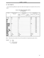
Table 4-2. Bus Interface Pin Operation List (3/3)
(c) Refresh cycle
Pin Name
Operation
A0 to A23
Note
D0 to D15
Note
WE
Note
OE
Note
RD
Note
ADV/BCYST
Note
UWR/UCAS
Note
LWR/LCAS
Note
IORD
Note
IOWR
Note
CS0 to CS7
Note
RAS0 to RAS7
Note
REFRQ
Note
WAIT
Maskable
HLDRQ
Maskable
HLDAK
Note
Note
Performs the same operation as the cycle that is generated by the target device program execution.
4.7
Emulation Memory Operation Timing Difference
When the area of the DRAM, synchronous flash memory, or page ROM in the target system has been allocated to
the emulation memory, the operation timing is the SRAM access timing.
When measuring the performance by using the emulation memory, adjust the setting so that the wait set matches
the memory access timing that is actually used.
Summary of Contents for IE-703102-MC-EM1
Page 2: ...2 MEMO ...
Page 10: ...10 MEMO ...
Page 24: ...24 MEMO ...
Page 26: ...26 MEMO ...
Page 34: ...34 MEMO ...
Page 40: ...40 MEMO ...
Page 46: ...46 MEMO ...
Page 48: ...48 MEMO ...

