


XR12 Troubleshooting Manual
Reading Electrical Schematics
Issue 3.0 2009-07-28
Page 5-3
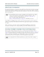
Structure of schematics
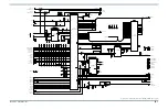
The electrical schematics are structured in a hierarchical format that is based on function and signal
flow. Wherever practical, the signal flow is from left to right. Normally, inputs originate on the left-
hand side and outputs extend to the right-hand side. Exceptions are shown by an arrow indicating the
direction of signal flow.
Figures
SD-1
through
SD-4
identify each major stage and its detailed interconnection. Each stage
contains cross-references that identify which block is the signal source for inputs or the destination
for outputs.
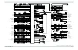
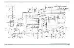
When a sub-function is treated as a block in Figures
SD-1
through
SD-4
, its detailed circuit
information is included in its own schematic drawing, which is also included in this section.
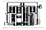
Locating schematic diagram for a functional block
The text inside a functional block provides the key to locating its schematic diagram. When a
functional block is assigned a reference designation, refer to the family trees in
, and follow the family tree branches to the block that contains the reference designation
and associated Nautel nomenclature (e.g., NAP34A). Refer to Table 5.1 with the Nautel
nomenclature number and the description to identify the appropriate figure number.
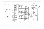
Note: The physical location of a part or assembly was not necessarily a factor during
creation of the schematic. The full reference designation assigned to a part or
assembly, in conjunction with the family tree (see
) and the assembly detail drawings (see
Section 6, “Mechanical Drawings” on page 6-1
), will identify its location.
Note: Schematics for some functional blocks may consist of more than one figure.
Summary of Contents for XR12
Page 2: ......
Page 4: ......
Page 8: ...XR12 Troubleshooting Manual Table of contents Page viii Issue 3 0 2009 07 28...
Page 12: ...XR12 Troubleshooting Manual Page xii Issue 3 0 2009 07 28...
Page 20: ...XR12 Troubleshooting Manual Page xx Issue 3 0 2009 07 28...
Page 100: ...XR12 Troubleshooting Manual Detailed Circuit Descriptions Page 2 32 Issue 3 0 2009 07 28...
Page 108: ...XR12 Troubleshooting Manual Parts Lists Page 3 8 Issue 3 0 2009 07 28...
Page 196: ......
Page 214: ...XR12 Troubleshooting Manual Reading Electrical Schematics Page 5 6 Issue 3 0 2009 07 28...
Page 223: ...Issue 3 1 2014 05 07 SD 9 Figure SD 9 NAPX05E 02 Dynamic Carrier Control PWB Sheet 1of 2...
Page 224: ...Issue 3 1 2014 05 07 SD 10 Figure SD 10 NAPX05E 02 Dynamic Carrier Control PWB Sheet 2 of 2...
Page 233: ...Issue 3 1 2014 05 07 SD 19 Figure SD 19 NAP34A RF Power Module Overall Sheet 1 of 2...
Page 234: ...Issue 3 1 2014 05 07 SD 20 Figure SD 20 NAP34A RF Power Module Modulator Stage Sheet 2 of 2...
Page 235: ...Issue 3 1 2014 05 07 SD 21 Figure SD 21 NAPC150A RF Drive Control PWB Sheet 1 of 3...
Page 236: ...Issue 3 1 2014 05 07 SD 22 Figure SD 22 NAPC150A RF Drive Control PWB Sheet 2 of 3...
Page 237: ...Issue 3 1 2014 05 07 SD 23 Figure SD 23 NAPC150A RF Drive Control PWB Sheet 3 of 3...
Page 238: ...Issue 3 1 2014 05 07 SD 24 Figure SD 24 NASM07H Modulator Assembly...
Page 239: ...Issue 3 1 2014 05 07 SD 25 Figure SD 25 NAA51A 03 RF Amplifier Assembly...
Page 245: ...Issue 3 1 2014 05 07 SD 31 Figure SD 31 NAPS10C RF Drive Power Supply PWB...
Page 248: ...Issue 3 0 2009 07 28 MD 1 Figure MD 1 XR12 Transmitter...
Page 257: ...Issue 3 0 2009 07 28 MD 10 Figure MD 10 NAPP02 01A RF Current Probe PWB...
Page 259: ...Issue 3 0 2009 07 28 MD 12 Figure MD 12 NAFP103 05 Forward Reflected Power Probe A1 DETAIL...
Page 263: ...Issue 3 0 2009 07 28 MD 16 Figure MD 16 NAPC150A RF Drive Control PWB...
Page 265: ...Issue 3 0 2009 07 28 MD 18 Figure MD 18 NASM07H Modulator Assembly...
Page 266: ...Issue 3 0 2009 07 28 MD 19 Figure MD 19 PA Input Output PWB 176 1065 04 and 05...
Page 267: ...Issue 3 0 2009 07 28 MD 20 Figure MD 20 NAA51A 03 RF Amplifier Assembly...
Page 268: ...Issue 3 0 2009 07 28 MD 21 Figure MD 21 NAPI47B Modulator Input Output PWB...
Page 271: ...Issue 3 0 2009 07 28 MD 24 Figure MD 24 Relay Assy 202 7019...
Page 272: ...Issue 3 0 2009 07 28 MD 25 Figure MD 25 Fan Tray 202 7020 J1 B1 B2...
Page 273: ...Issue 3 0 2009 07 28 MD 26 Figure MD 26 NAPS10C RF Drive Power Supply 62 V...
Page 275: ...Issue 3 0 2009 07 28 MD 28 Figure MD 28 Rectifier Assembly 202 7017...
Page 282: ......