LMK03002C
Precision Clock Conditioner with Integrated VCO
Evaluation Board Operating Instructions
7-23-2007
National Semiconductor Corporation
Interface
2900 Semiconductor Dr.
MS A2-600
Santa Clara, CA, 95052-8090
Page 1: ...3002C Precision Clock Conditioner with Integrated VCO Evaluation Board Operating Instructions 7 23 2007 National Semiconductor Corporation Interface 2900 Semiconductor Dr MS A2 600 Santa Clara CA 95052 8090 ...
Page 2: ...C OPERATION 4 BOARD INFORMATION 8 OSCin 8 Fout 8 Loop Filter 8 Features of the board 9 Other Important Notes 9 RECOMMENDED EQUIPMENT 10 PHASE NOISE 11 DELAYS 12 CODELOADER SETTINGS 13 APPENDIX A VCO PERFORMANCE 17 Loop Filter 2 17 APPENDIX B IMPACT OF REFERENCE ON PHASE NOISE 19 APPENDIX C SCHEMATICS 20 APPENDIX D BILL OF MATERIALS 23 APPENDIX E BUILD DIAGRAM 25 ...
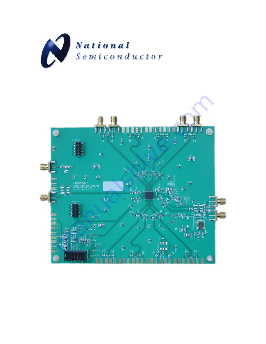
Page 3: ...ks for many LMK0300xC devices Because of this the silkscreen on the board is different from actual clock outputs in the datasheet and in CodeLoader Refer to the table below for the correct mapping Datasheet CodeLoader LMK0300xC EVB PCB CLKout0 CLKout0 CLKout4 CLKout4 CLKout1 CLKout1 CLKout5 CLKout5 CLKout2 CLKout2 CLKout6 CLKout6 CLKout3 CLKout3 CLKout7 CLKout7 Loop Filter 1 Phase Margin 63º Kφ φ ...
Page 4: ...lling CodeLoader 4 USB Driver for instructions to prepare the computer for usage with the evaluation board before continuing with the hardware setup For basic operation 1 Connect a low noise 3 3 V power supply to the Vcc connector located at the top left of the board 2 Connect the CodeLoader cable to the uWire header located in the lower left ...
Page 5: ...LPT to uWire cable plugging the cable into an LPT port on the computer and then the 10 pin ribbon connector to the evaluation board This setup is shown below The cable can be removed after programming to minimize noise and EMI or Available separately the USB uWire board to the PC with the USB cable and the USB uWire board to the evaluation board with the 10 pin ribbon cable LPT Setup ...
Page 6: ...A R D O P E R A T I N G I N S T R U C T I O N S 6 Read first Basic Operation Continued 4 Start CodeLoader 4 5 Select the USB or LPT Communication Mode on the Port Setup tab as appropriate 6 Select the default mode by clicking Mode 16 MHz OSCin ...
Page 7: ... Continued 7 Enable output to be measured any of CLKout 0 7 or EN_Fout from either Clock Outputs or Bits Pins tab 8 Program the part by clicking Keyboard Controls Load Device or by pressing Ctrl L 9 Make measurements After programming the uWire cable can be unplugged from the evaluation board to minimize noise and EMI ...
Page 8: ... setup 0 ohm R7 R8 R10 R13 100 ohm R17 0 1 uF C5 C35 C36 is a 0 1 uF 0402 cap which may be moved to C5 Open C4 C36 R11 R12 R14 R15 R16 R79 R20 remove power from crystal oscillator for noise reasons Single ended OSCin setup 0 ohm R7 R8 51 ohm R15 0 1 uF C35 C36 C5 is a 0 1 uF 0402 cap which may be moved to C36 Open C4 C5 R10 R11 R12 R13 R14 R16 R17 R79 R20 remove power from crystal oscillator for n...
Page 9: ...r on the upper left side of the board Vcc is located on VccPlane test point located to the right of the Vcc SMA Vcc is located on the bottom side of the board on each pad of the unstuffed 10 pin header VCC_J2 Other Important Notes When changing the OSCin frequency the OSCin frequency register needs to be changed to match Toggle the SYNC pin to synchronize the clock outputs when in divided mode For...
Page 10: ...easurements At frequencies less than 100 MHz the local oscillator noise of the PSA is too high and measurements will be of the local oscillator not the device under test Oscilloscope For measuring delay an Agilent Infiniium DSO81204A was used Reference Oscillator The on board crystal oscillator will provide a low noise reference signal to the device at offsets greater than 1 kHz Note The default l...
Page 11: ... integrated RMS jitter 474 fs 100 Hz 20 MHz integrated RMS jitter 202 fs 12 kHz 20 MHz integrated RMS jitter 188 fs shown LVPECL output CLKout0 Labeled CLKout4 on EVB VCO Frequency 1632 MHz VCO_DIV 2 CLKout0_div 4 LVPECL output 204 MHz Reference source is on board 16 MHz crystal Below 1 kHz phase noise is dominated by the crystal 10 Hz 20 MHz integrated RMS jitter 636 fs 100 Hz 20 MHz integrated R...
Page 12: ... These delay measurements illustrate how skew errors due to different length traces may be tuned out The delay may be adjusted in steps of 150 ps Delays 150 300 450 600 750 CLKout0_DLY 0 ps CLKout1_DLY all delays programmed 0 150 300 450 600 750 900 1050 1200 1350 1500 1650 1800 1950 2100 and 2250 ps ...
Page 13: ...ignals are assigned to which pins If this is wrong the part will not program Part setup can be restored to the default state by clicking Mode 16 MHz OSCin The default reference oscillator used for these instructions is 16 MHz and the restored mode expects a 16 MHz OSCin signal For the loaded mode to take affect the device must be loaded by pressing Ctrl L ...
Page 14: ...g DIV4 Shall be checked for OSCin frequencies greater than 20 MHz RESET The registers can be defaulted by checking and unchecking RESET Software bits will not reflect this VCO_R3_LF VCO_R4_LF VCO_C3_C4_LF Internal loop filter values also accessible from Clock Outputs tab EN_CLKout0 3 Enable CLKout bits from CLKout0 to CLKout7 Also accessible from Clock Outputs tab EN_CLKout_Global Enable all clock...
Page 15: ... or Ctrl L The Clock Outputs tab allows the user to visualize the clock distribution portions of the device From this tab the device s dividers delays clock output muxes and output drivers can be programmed along with internal loop filter values The PLL block shows the R and N divider values however to change these values either click on the PLL tab or the blue PLL box to access the PLL tab to mak...
Page 16: ...etector Frequency VCO Divider Depending on the situation this may require the R Counter multiplied up by the value of the VCO Divider to achieve desired VCO output frequencies Example If the desired VCO output frequency was 1648 MHz R would need to be increased to 2 before 1648 MHz could be programmed because of the VCO Divider of 2 would only allow programming of 1600 1632 1664 etc with a 16 MHz ...
Page 17: ...switching between the two different loop filters Loop Filter 2 Phase Margin 58º Kφ φ φ φ 100 uA Loop Bandwidth 55 Hz Fcomp 500 kHz Crystal Frequency 16 MHz Output Frequency 1566 to 1724 MHz Supply Voltage 3 3 Volts VCO Gain 13 MHz Volt VCO 820 nF 10 uF 820 Ω Ω Ω Ω 150 pF 110 pF 600 Ω Ω Ω Ω 200 Ω Ω Ω Ω CPout Charge Pump C1 C2 R2 R3 R4 C3 C4 This loop filter is located on the top side of the PCB and...
Page 18: ...etector Frequency An external oscillator was used for this plot since the VCO noise dominates reference oscillator noise is not critical The loop bandwidth has been minimized so that the VCO is the dominant noise contributor 10 Hz 20 MHz integrated RMS jitter 107 6 ps 100 Hz 20 MHz integrated RMS jitter 28 1 ps shown 1 kHz 20 MHz integrated RMS jitter 2 7 ps 12 kHz 20 MHz integrated RMS jitter 0 3...
Page 19: ...n ultra low jitter 100 MHz Wetzel Crystal 501 04517D and setting R 5 to achieve a phase detector frequency of 20 MHz A very low integrated RMS jitter of 201 fs is measured vs the 474 fs measured in the Phase Noise section with 16 MHz crystal in the bandwidth of 10 Hz to 20 MHz 10 Hz 20 MHz integrated RMS jitter 201 fs shown 100 Hz 20 MHz integrated RMS jitter 197 fs 1 kHz 20 MHz integrated RMS jit...
Page 20: ... C T I O N S 20 Appendix C Schematics LMK0300x Main Board LMK0300x Main Board sch LMK0300x Outputs LMK0300x Outputs sch F1 PCB_LMK0300x 1 2 3 4 5 6 7 8 9 10 J2 GND_HDR 1 2 3 4 5 6 7 8 9 10 J3 VCC_HDR Vcc Vcc 1 2 3 4 5 6 7 8 9 10 J4 GND_HDR 1 2 3 4 5 6 7 8 9 10 J5 VCC_HDR Vcc Vcc ...
Page 21: ...31 CPout 32 Vcc10 33 NC 34 NC 35 Bias 36 Vcc11 37 CLKout4 38 CLKout4 39 Vcc12 40 CLKout5 41 CLKout5 42 Vcc13 43 CLKout6 44 CLKout6 45 Vcc14 46 CLKout7 47 CLKout7 48 U1 LMK0300XC CLKuWire DATAuWire LEuWire LEuWire DATAuWire CLKuWire Vcc DUT_OSCin DUT_OSCin R95 0 ohm R94 0 ohm C69 1 uF OSCin SMA OSCin SMA P 1 Pd 3 S 4 S ct 5 Sd 6 NC 2 B1 Open DUT_OSCin DUT_OSCin TCXO_RF R7 Open R10 Open R11 0 ohm R1...
Page 22: ...Open CLKout1 CLKout1 Vcc Vcc CLKout6 OpenSMA CLKout6 OpenSMA R73 Open R71 Open R72 Open R69 Open R70 Open C64 0 1 uF C65 0 1 uF R101 120 ohm R100 120 ohm CLKout6 CLKout6 Vcc Vcc CLKout2 OpenSMA CLKout2 SMA R51 Open R49 Open R50 Open R47 Open R48 Open C56 0 1 uF C57 0 1 uF R46 Open R45 Open CLKout2 CLKout2 Vcc Vcc CLKout7 SMA CLKout7 SMA R78 Open R76 Open R77 Open R74 Open R75 Open C66 0 1 uF C67 0...
Page 23: ...0 nF Kemet C0603C824K8PAC 1 C1_AUX 1 uF Kemet C0603C105K8VAC 16 C69 C70 C71 C72 C73 C74 C75 C76 C77 C79 C80 C81 C82 C83 C84 C85 10 uF Kemet C0805C106K9PAC 5 C2p_AUX C16 C17 C18 C19 10 uF Kemet C0805C106K9PAC 1 C78 Resistors 0 ohm Vishay CRCW0603000ZRT1 10 R1 R3 R6 R11 R12 R20 R22 R95 R104 R109 0 ohm Yageo RC0805JR 070RL 2 R4 R8 0 ohm Vishay CRCW0603000ZRT1 2 R87 R94 18 ohm Vishay CRCW0603180JRT1 1...
Page 24: ...DER_2X5 POLARIZED FCI Electronics 52601 S10 8 1 uWire SPCS 8 SPC Technology SPCS 8 4 Standoffs in the four corners insert from bottom Open Open Open 2 B1 B2 Open 603 32 C1 C2_AUX C6 C7 C8 C10 C11 C12 C13 C14 C15 R5 R7 R10 R14 R16 R17 R18 R19 R21 R23 R24 R25 R26 R27 R28 R79 R105 R107 R110 R111 R112 Open 805 1 C2p Open Open 1 C3 Open 402 16 C4 C5 R31 R32 R37 R38 R39 R44 R45 R46 R51 R58 R63 R68 R73 R...
Page 25: ...L M K 0 3 0 0 2 C E V A L U A T I O N B O A R D O P E R A T I N G I N S T R U C T I O N S 25 Appendix E Build Diagram ...
Page 26: ...L M K 0 3 0 0 2 C E V A L U A T I O N B O A R D O P E R A T I N G I N S T R U C T I O N S 26 Bottom Build Diagram ...
Page 27: ...for use in safety critical applications such as life support where a failure of the TI product would reasonably be expected to cause severe personal injury or death unless officers of the parties have executed an agreement specifically governing such use Buyers represent that they have all necessary expertise in the safety and regulatory ramifications of their applications and acknowledge and agre...
Page 28: ...андарту ISO 9001 Лицензия ФСБ на осуществление работ с использованием сведений составляющих государственную тайну Поставка специализированных компонентов Xilinx Altera Analog Devices Intersil Interpoint Microsemi Aeroflex Peregrine Syfer Eurofarad Texas Instrument Miteq Cobham E2V MA COM Hittite Mini Circuits General Dynamics и др Помимо этого одним из направлений компании ЭлектроПласт является на...