background image

Appendix E

SCXI-1121 Cabling

SCXI-1121 User Manual

E-10

www.natinst.com

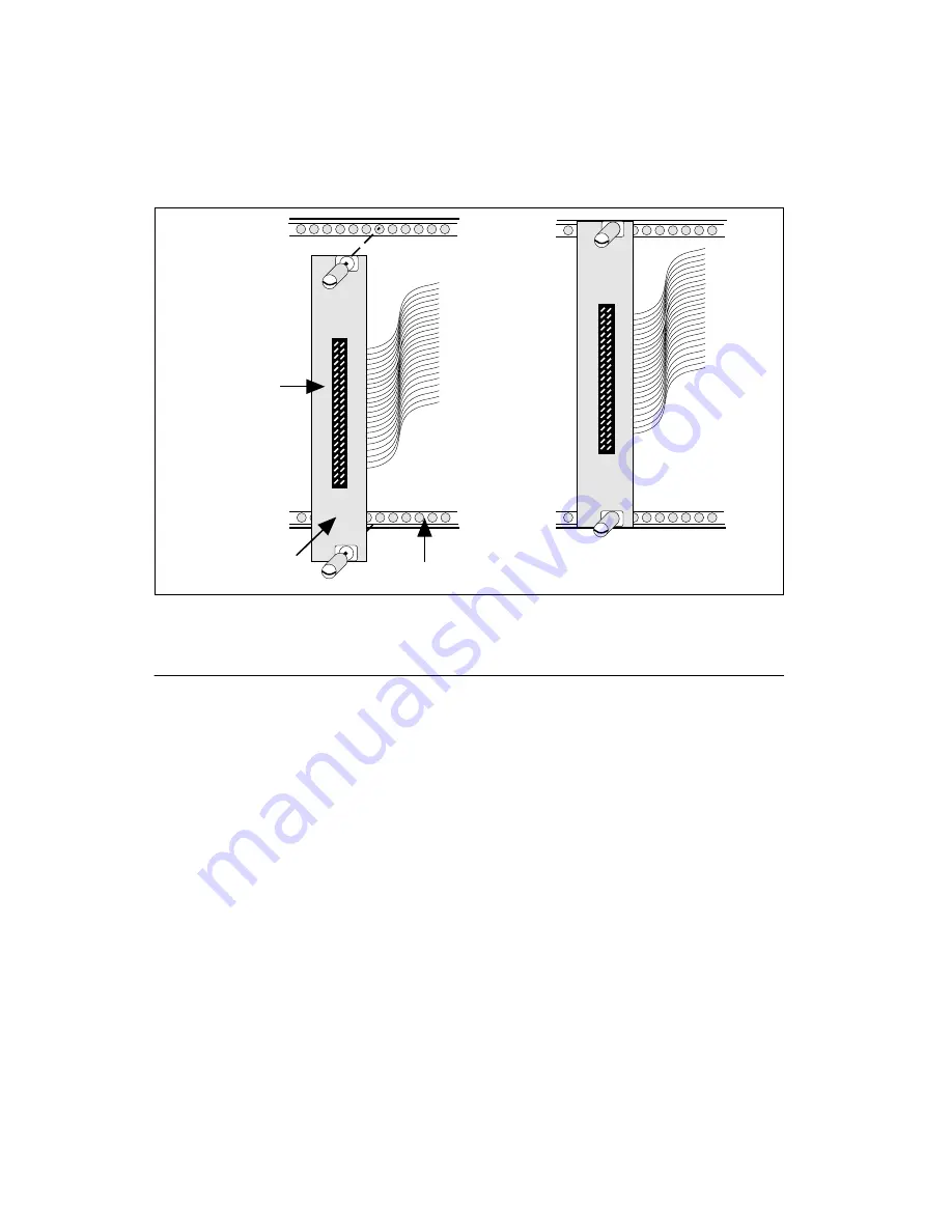
Figure E-3.  

SCXI-1180 Front Panel Installation

SCXI-1302 50-Pin Terminal Block

The SCXI-1302 terminal block has screw terminal connections for the 
50-pin connector on the SCXI-1180 feedthrough panel.

SCXI-1302 Wiring Procedure

To wire the SCXI-1302 terminal block, you must remove the cover, connect 
all the wiring, and replace the cover. The procedure for this is as follows:

1.

Unscrew the rear grounding screw on the back of the terminal block, 
as shown in Figure E-4.

2.

With a flathead screwdriver, carefully pry the cover off the terminal 
block. 

3.

Insert each wire through the terminal block strain-relief opening.

4.

Connect the wires to the screw terminals.

5.

Tighten the large strain-relief screws to secure the wires.

Front Panel 
Connector

Front Panel

Front Threaded Strip

Ribbon Cable to 
Rear and Breakout 
Connectors

Step 5

Summary of Contents for SCXI-1121

Page 1: ...SCXI SCXI 1121 User Manual Four Channel Isolated Universal Transducer Module for Signal Conditioning SCXI 1121 User Manual September 1999 Edition Part Number 320426C 01...

Page 2: ...1 48 14 24 24 Germany 089 741 31 30 Greece 30 1 42 96 427 Hong Kong 2645 3186 India 91805275406 Israel 03 6120092 Italy 02 413091 Japan 03 5472 2970 Korea 02 596 7456 Mexico D F 5 280 7625 Mexico Mont...

Page 3: ...vents outside reasonable control Copyright Under the copyright laws this publication may not be reproduced or transmitted in any form electronic or mechanical including photocopying recording storing...

Page 4: ...Configuration 2 6 Grounding Shielding and Reference Mode Selection 2 6 Input Channel Jumpers 2 8 Excitation Jumpers 2 9 Hardware Installation 2 14 Signal Connections 2 15 Front Connector 2 16 Front C...

Page 5: ...canning Modes 3 17 Single Module Parallel Scanning 3 17 Multiplexed Scanning 3 17 Single Module Multiplexed Scanning 3 18 Multiple Module Multiplexed Scanning 3 19 Multiple Chassis Scanning 3 20 Chapt...

Page 6: ...riggering and Servicing 5 14 Scanning Examples 5 15 Example 1 5 15 Example 2 5 15 Example 3 5 16 Appendix A Specifications Appendix B Rear Signal Connector Appendix C SCXIbus Connector Appendix D SCXI...

Page 7: ...14 SCXI 1121 Rear Signal Connector Pin Assignment 2 39 Figure 2 15 SCANCLK Timing Requirements 2 43 Figure 2 16 Slot Select Timing Diagram 2 44 Figure 2 17 Serial Data Timing Diagram 2 45 Figure 2 18...

Page 8: ...8 Excitation Level Jumper Selection 2 12 Table 2 9 Completion Network Jumpers 2 14 Table 2 10 Trimmer Potentiometer and Corresponding Channel 2 27 Table 2 11 Nulling Resistors and Corresponding Channe...

Page 9: ...via jumpers This manual describes the installation basic programming considerations and theory of operation for the SCXI 1121 Conventions The following conventions appear in this manual Angle brackets...

Page 10: ...uments contain information that you may find helpful as you read this manual AT MIO 16 User Manual part number 320476 01 AT MIO 16D User Manual part number 320489 01 AT MIO 16F 5 User Manual part numb...

Page 11: ...CXI systems However the Lab PC cannot control multiple chassis SCXI systems You can use the Lab NB the Lab PC the Lab LC and the PC LPM 16 boards with the SCXI 1121 but these boards can control only s...

Page 12: ...s for data acquisition instrument control data analysis and graphical data presentation Your National Instruments data acquisition board is shipped with the NI DAQ software NI DAQ has a library of fun...

Page 13: ...ul graphical programming language The LabVIEW Data Acquisition VI Library a series of VIs for using LabVIEW with National Instruments boards is included with LabVIEW The LabVIEW Data Acquisition VI Li...

Page 14: ...able assembly 776574 41 SCXI 1342 PC LPM 16 cable assembly 776574 42 SCXI 1343 rear screw terminal adapter 776574 43 SCXI 1344 Lab LC cable assembly 776574 44 SCXI 1346 shielded multichassis cable ada...

Page 15: ...on 3M part number 3425 7650 T B Ansley Corporation part number 609 5041CE Standard 50 conductor 28 AWG stranded ribbon cables that can be used with these connectors are as follows Electronic Products...

Page 16: ...rostatic discharge To avoid such damage in handling the module take the following precautions Touch the antistatic package to a metal part of your SCXI chassis before removing the module from the pack...

Page 17: ...the SCXI 1121 jumper configurations installation of the SCXI 1121 into the SCXI chassis signal connections to the SCXI 1121 and cable wiring Module Configuration The SCXI 1121 contains 49 jumpers tha...

Page 18: ...OT0SEL signal from the rear signal connector after buffering to the SCXIbus INTR line and should be left in the factory set position position 1 On Revision C or later modules jumper W44 does not exist...

Page 19: ...ers W1 and W2 W17 and W18 W27 and W28 and W39 and W40 configure the half bridge completion network for channels 0 through 3 respectively Further configuration of the board is software controlled and w...

Page 20: ...er modules Position 1 connects a 2 2 k pullup resistor to the SERDATOUT line factory default setting and Position 3 does not connect the pullup resistor to the SERDATOUT line Using Jumpers W32 and W38...

Page 21: ...umper W32 is not used You set jumper W38 as explained in the cases above except in the case of a multiple chassis ribbon cable system In a multichassis ribbon cable system with Revision A and B SCXI 1...

Page 22: ...and Reference Mode Selection Jumper W33 Position AB R0 connects the analog reference to the analog output ground pins 1 and 2 on the rear signal connector Select this configuration if you are using a...

Page 23: ...rate with data acquisition boards that have a nonreferenced single ended NRSE input It is not recommended to use differential input data acquisition boards when jumper W33 is in the AB R2 position Tab...

Page 24: ...stage gain set to 10 position D To change the gain of your module move the appropriate jumper on your module to the position indicated in Table 2 4 Refer to Figure 2 2 for the jumper locations on your...

Page 25: ...ays make sure to set both stages to the same bandwidth This will ensure that the required bandwidth is achieved Excitation Jumpers Current and Voltage Excitation Jumpers You can configure each excitat...

Page 26: ...t you should select the level of excitation according to the load you are using Table 2 7 lists the maximum load that can be driven per channel at each level of excitation for both volt and current ex...

Page 27: ...ith the Voltage mode set to 3 333 V Table 2 7 Maximum Load per Excitation Channel Excitation Level Maximum Load 3 333 V 28 mA 10 V 14 mA 0 150 mA 10 k 0 450 mA 10 k Table 2 8 Excitation Level Jumper S...

Page 28: ...When the completion network is enabled you cannot access the negative input of the amplifier which preserves the overvoltage protection of the channel Table 2 9 shows how to enable and disable the co...

Page 29: ...ents Corporation 2 13 SCXI 1121 User Manual 2 W27 and W28 3 W39 and W40 Table 2 9 Completion Network Jumpers Continued Channel Jumpers Enable Completion Disable Network Factory Setting A B W28 W27 1 2...

Page 30: ...Gently guide the module into the back of the slot until the connectors make good contact If a cable assembly has already been installed in the rear of the chassis the module and cable assembly must b...

Page 31: ...rate damaged equipment The safety protection features built into this device can become impaired if the device becomes damaged in any way If the device is damaged turn the device off and do not use un...

Page 32: ...must connect a safety earth ground wire to the terminal block safety ground solder lug This complies with safety agency requirements and protects against electric shock when the terminal block is not...

Page 33: ...e 2 3 SCXI 1121 Front Connector Pin Assignment Pin Number Signal Name Column A B C Signal Name 32 31 30 29 28 27 26 25 24 23 22 21 20 19 18 17 16 15 14 13 12 11 10 9 8 7 6 5 4 3 2 1 CGND 5 V EGND2 EX1...

Page 34: ...ed C6 C8 RSVD Reserved These pins are reserved Do not connect any signal to these pins A8 C10 C16 C22 C28 No Connect Do not connect any signal to these pins A10 EGND3 Excitation Ground 3 This pin conn...

Page 35: ...is connected to the excitation channel 1 positive output C24 EX1 Negative Excitation Output 1 This pin is connected to the excitation channel 1 negative output A26 CH1 Positive Input Channel 1 This pi...

Page 36: ...ced to a ground level with common mode voltage up to 250 Vrms For better noise immunity connect the negative input channel to the signal reference If the measured signals are floating connect the nega...

Page 37: ...o the input bias current and to the resistor value used The typical input bias current of the amplifier consists of 80 pA and a negligible offset drift current When a 100 k resistor is used this will...

Page 38: ...or connecting the temperature sensor to the SCXI 1121 The temperature sensor is not isolated and is referenced to chassis ground The connection is overvoltage protected to 25 VDC with power on and 15...

Page 39: ...need long nose pliers to insert the washer and nut 8 Tighten the nut by holding it firmly and rotating the jack screw 9 Repeat steps 6 through 8 for the second jack screw 10 Replace the module cover a...

Page 40: ...Warnings When using the terminal block with high common mode voltages you must insulate your signal wires appropriately National Instruments is not liable for any damages or injuries resulting from i...

Page 41: ...figurations Each channel has its own nulling circuitry and its own trimming potentiometer as listed in Table 2 10 To null the static offset voltage of the bridge use the following procedure 1 Configur...

Page 42: ...ollowing formula refer to Figure 2 9 for visual help where Rg is the nominal strain gauge resistance value Rd is either a completion resistor or a second strain gauge nominal resistance Rnull is the n...

Page 43: ...g Circuit Using the SCXI 1321 with RTDs and Thermistors When using this terminal block with RTDs or thermistor type transducers and with the SCXI 1121 excitation set in the Current mode you must disab...

Page 44: ...nfiguration places a shunting resistor in parallel with the strain gauge as shown in Figure 2 10 Table 2 12 Jumper Settings of the Nulling Circuits Jumper Position Description W1 Nulling circuit of Ch...

Page 45: ...ng resistor is 199 Determine the change as follows 1 Determine the change caused by the shunting resistor using the following formula 2 Using the appropriate strain gauge strain formula and assuming t...

Page 46: ...via MCH4 pins 11 and 12 on the module rear signal connector This is the Direct Temperature Sensor DTS mode Note Use an average of a large number of samples to obtain the most accurate reading Noisy en...

Page 47: ...I 1121 output multiplexer This is the factory setting The DTEMP position of jumper W1 jumper W5 on the SCXI 1321 connects the temperature sensor to the SCXI 1121 MCH4 signal on the rear signal connect...

Page 48: ...ion W1 MTS mode selected factory setting parking position W1 DTS mode selected Table 2 14 Jumper Settings on the SCXI 1328 Terminal Block Jumper Position Description W1 MTS mode selected factory setti...

Page 49: ...ect all power before removing cover Always install grounding screw To connect the signal to the terminal block use the following procedure 1 Remove the grounding screw of the top cover 2 Snap out the...

Page 50: ...Chapter 2 Configuration and Installation SCXI 1121 User Manual 2 34 www natinst com Figure 2 11 SCXI 1320 Parts Locator Diagram...

Page 51: ...Chapter 2 Configuration and Installation National Instruments Corporation 2 35 SCXI 1121 User Manual Figure 2 12 SCXI 1328 Parts Locator Diagram...

Page 52: ...terminal block to the SCXI 1121 front connector perform the following steps 1 Connect the SCXI 1121 front connector to its mating connector on the terminal block 2 Make sure that the SCXI 1121 top and...

Page 53: ...1343 rear screw terminal adapter or the SCXI 1351 one slot cable extender with the SCXI 1121 you should read this section Figure 2 14 shows the pin assignments for the SCXI 1121 rear signal connector...

Page 54: ...l input data to a module or Slot 0 26 SERDATOUT Serial Data Out This signal taps into the SCXIbus MISO line to accept serial output data from a module 27 DAQD A Data Acquisition Board Data Address Lin...

Page 55: ...ced single ended RSE measurements W33 should be in position AB R0 to connect the SCXI 1121 ground to the data acquisition analog ground Pin 19 is the OUTREF pin this pin is connected internally to the...

Page 56: ...AQD A 0 or address DAQD A 1 information Pin 29 is SLOT0SEL and is equivalent to the SCXIbus INTR line It indicates whether the data on the SERDATIN line is being sent to Slot 0 SLOT0SEL 0 or to a modu...

Page 57: ...Input rating 5 5 V with respect to DIG GND Digital input specifications referenced to DIG GND VIH input logic high voltage 2 V minimum VIL input logic low voltage 0 8 V maximum II input current leakag...

Page 58: ...o be discussed For information on the Slot 0 Slot Select Register consult Chapter 4 Register Descriptions The data acquisition board determines to which slot it will talk by writing a slot select numb...

Page 59: ...o 1 This will assert the SS line of the module whose slot number was written to Slot 0 If multiple chassis are being used only the appropriate slot in the chassis whose address corresponds to the writ...

Page 60: ...Slot Select After the 32 bits of data are read from the Module ID Register further data will be zeros until reinitialization occurs To write to the Configuration Register follow these steps 1 Initial...

Page 61: ...ite Timing Diagram To read from the Module ID Register follow these steps 1 Initial conditions SS asserted low SERDATIN don t care DAQD A 1 Make sure DAQD A does not go low or erroneous data will be w...

Page 62: ...le ID Register Figure 2 19 SCXI 1121 Module ID Register Timing Diagram For further details on programming these signals refer to Chapter 5 Programming SLOT0SEL SS SERCLK 0 0 0 0 0 0 0 0 0 0 0 0 0 0 0...

Page 63: ...unit making up the SCXI 1121 Functional Overview The block diagram in Figure 3 1 illustrates the key functional components of the SCXI 1121 Figure 3 1 SCXI 1121 Block Diagram SCXIbus Digital Interface...

Page 64: ...XI 1121 consists of four isolated amplifier channels with gains of 1 2 5 10 20 50 100 200 500 1 000 and 2 000 and four isolated excitation channels with voltage or current excitation The SCXI 1121 als...

Page 65: ...15 B15 A16 B16 A17 B17 A18 B18 A19 B19 A20 B20 A21 B21 A22 B22 A23 B23 A24 B24 D1 C1 D2 C2 D3 C3 D4 C4 D5 C5 D6 C6 D7 C7 D8 C8 D9 C9 D10 C10 D11 C11 D12 C12 D13 C13 D14 C14 D15 C15 D16 C16 D17 C17 D18...

Page 66: ...ializes the module to its power up state Totem pole Input B19 MISO Master In Slave Out Transmits data from the module to the SCXIbus Open collector I O C19 D A Data Address Indicates to the module whe...

Page 67: ...assis In order for the data acquisition board to talk to a slot the board must first assert the SS for that slot This is done by asserting INTR low writing a 16 bit number over MOSI corresponding to t...

Page 68: ...try Block Diagram The digital interface circuitry is divided into a data acquisition section and an SCXIbus section The SCXI 1121 connects to the SCXIbus via a 4 24 metral receptacle and to the data a...

Page 69: ...ovides temperature channel selection and channel selection and configures the SCXI 1121 for scanning options All the control bits are fed into a latch before being routed to the rest of the module The...

Page 70: ...ten to MISO thereafter until SS is released and reasserted The SCXI 1121 module ID is hex 00000002 Analog and Timing Circuitry The SCXIbus provides analog power 18 5 VDC that is regulated on the SCXI...

Page 71: ...n 3 9 SCXI 1121 User Manual Figure 3 5 Analog Input Block Diagram Input Channel 1 Input Channel 2 Input Channel 3 MTEMP DTEMP Input Channel 0 LPF I To Output Stage LPF LPF To Output Stage LPF To Outpu...

Page 72: ...kHz and G is the gain at this stage This BW might be of concern at high first stage gains such as 50 and 100 In this case the first stage amplifier has a BW equal to 16 kHz and 8 kHz respectively Bec...

Page 73: ...de you can set the level to 150 A or 450 A You can choose one configuration out of the four available To configure the excitation channels refer to Chapter 2 Configuration and Installation The excitat...

Page 74: ...tiometers dedicated for calibration For the amplifier channels one potentiometer is used to null the output offset the other is used to null the input offset On the excitation channels one potentiomet...

Page 75: ...rd the exact value you have measured 2 Set up the excitation channel of interest to 3 333 V excitation level 3 Connect your DMM leads to the excitation output as close as possible to the resistor body...

Page 76: ...lacquer to avoid tampering with the calibration Table 3 2 lists the potentiometer reference designators that correspond to each channel The resistor used to calibrate the current level must be a preci...

Page 77: ...annels is to be connected to MCH0 In the Single Channel Read mode the MUXCOUNTER is loaded with the desired channel number In the Scanning mode the counter is loaded with the first channel to be read...

Page 78: ...tiplexed output of the SCXI 1121 via switches to AB0 on the SCXIbus and on to other modules When you use multiple modules you can bus the output of the module via AB0 to the module that is connected t...

Page 79: ...g because the module provides all channels to the data acquisition board at all times You can implement single module parallel scanning with any data acquisition board that is appropriately cabled to...

Page 80: ...arting channel Notice that although you are using only a single module you can put many entries with different counts in the Slot 0 FIFO so that some channels are read more often than others You canno...

Page 81: ...les and Slot 0 as illustrated in Figure 3 10 The scan list in Slot 0 is programmed with the sequence of modules and the number of samples per entry Figure 3 10 Multiple Module Multiplexed Scanning Cab...

Page 82: ...f Slot 13 to fill the samples when the data acquisition board will be sampling another chassis or data acquisition board channel This will keep the chassis synchronized Notice that you can only perfor...

Page 83: ...each bit The register bit map shows a diagram of the register with the MSB shown on the left bit 15 for a 16 bit register bit 7 for an 8 bit register and the LSB shown on the right bit 0 A rectangle...

Page 84: ...ast significant byte first Within each byte data is sent out most significant bit first Additional data transfers will result in all zeros being sent on the MISO line The Module ID Register is reiniti...

Page 85: ...al If CLKOUTEN is set to 1 SCANCLK is transmitted on TRIG0 If CLKOUTEN is cleared to 0 SCANCLK is not transmitted on TRIG0 14 CLKSELECT Scanclock Select This bit determines whether the SCXI 1121 uses...

Page 86: ...ut The module output will only be driven when FOUTEN is cleared to 0 or SCANCON is active low while SCANCONEN is cleared 4 RSVD Reserved This bit should always be written to zero 3 SCANCLKEN Scan Cloc...

Page 87: ...ect Register also determines in which chassis the desired slot is The FIFO Register is a 16 bit write only register used for storing the Slot 0 scan list that determines the chassis scan sequence The...

Page 88: ...s number written The Slot Select Register will shift in the data present on the MOSI line bit 16 first when SLOT0SEL is cleared to zero Type Write only Word Size 16 bit Bit Map Bit Name Description 15...

Page 89: ...reprogrammed in two steps instead of having to rewrite the entire list When this bit is set it has no effect 5 RD Read This bit when clear prevents the FIFO from being read When set the FIFO is being...

Page 90: ...www natinst com 1 SCANCONEN Scan Control Enable When set this bit enables the SCANCON lines When clear all SCANCON lines are disabled high 0 CLKEN Clock Enable When set this bit enables TRIG0 as a clo...

Page 91: ...er The Slot 0 scan list is created by consecutive writes to the FIFO Register Each write creates a new entry at the end of the scan list The maximum number of entries is 256 To clear the FIFO of all e...

Page 92: ...on boards involves writes to their registers See your data acquisition board user manual for more information The programming instructions list the sequence of steps to take The instructions are langu...

Page 93: ...the remaining bits However a write to one of these registers will affect all bits simultaneously You cannot read the registers to determine which bits have been set or cleared in the past therefore y...

Page 94: ...u are writing to the HSCR or FIFO Register leave DAQD A high 6 For each bit to be written to the Configuration Register a Establish the desired SERDATIN level corresponding to this bit b Clear SERCLK...

Page 95: ...o account for the gains of both the SCXI 1121 and the data acquisition board when calculating the actual voltage present at the input of the SCXI 1121 To measure one of the four differential input cha...

Page 96: ...ster 2 Measure the voltage with the data acquisition board Indirect Measurements Indirect measurements involve one module sending a signal to Analog Bus 0 where it is picked up by another module and t...

Page 97: ...differential input channels of the SCXI 1121 perform the following steps 1 Perform any necessary programming to ensure that no modules are driving Analog Bus 0 For an SCXI 1121 clearing AB0EN in the C...

Page 98: ...support any of the multiplexed scanning modes Notice that single module parallel scanning is typically done without any module or Slot 0 programming only programming the data acquisition board is nece...

Page 99: ...ng Lab PC User Manual Programming Multiple A D Conversions with Channel Scanning Programming Multiple A D Conversions with Interval Scanning Programming Multiple A D Conversions in Single Channel Inte...

Page 100: ...e part called Program the Sample Interval Counter You will do this after you program the modules and Slot 0 Clear the A D Circuitry in the Lab PC User Manual the Lab PC User Manual and the PC LPM 16 U...

Page 101: ...nter 1 8 Set the SCANDIV bit in Command Register 1 2 Module Programming This section describes the programming steps for various scanning possibilities For all the bit patterns in this section Sc sign...

Page 102: ...ing steps are as follows 1 Perform any necessary programming to ensure that no modules are driving Analog Bus 0 For an SCXI 1121 clearing AB0EN in the Configuration Register will ensure that its outpu...

Page 103: ...n board but not drive Analog Bus 0 unless it is receiving an active low signal on SCANCON Also program the module to send a SCANCLK compatible signal onto TRIG0 If this module is an SCXI 1121 this pro...

Page 104: ...es according to Channel Scanning from the SCXI 1121 via Another Module earlier in this chapter 3 Programming the Slot 0 Hardscan Circuitry The following section describes how to program the Slot 0 cir...

Page 105: ...r each entry Thus two entries with counts of two for one module will yield different behavior than one entry with a count of four For multiple chassis scanning program each Slot 0 with dummy entries t...

Page 106: ...is chapter 2 Following the procedure given in the Register Writes section write 10000001 00001101 to the Configuration Register of the SCXI 1121 in Slot 1 3 Follow the steps outlined in the section ea...

Page 107: ...lot 3 Notice that after Channel 3 the SCXI 1121 will wrap around to Channel 0 6 Follow the steps given in the section earlier in this chapter 3 Programming the Slot 0 Hardscan Circuitry where step 3 W...

Page 108: ...MOSI 3 Toggle SLOT0SEL 4 Write XXXXX110 00000101 over MOSI 5 Select Slot 14 in Chassis 2 6 Write XXXXX110 00000011 over MOSI 7 Toggle SLOT0SEL 8 Write XXXXX101 00000001 over MOSI 9 Toggle SLOT0SEL 10...

Page 109: ...0 100 200 500 1 000 2 000 Output range 5 V Number of channels 4 Gain accuracy1 0 15 of full scale Offset voltage Input 6 V Output 3 mV Stability versus ambient temperature Input offset drift 0 2 V C O...

Page 110: ...5 accuracy 20 sec Rise time 4 Hz 0 12 sec 10 kHz 70 sec Slew rate 0 15 V sec Operating common mode voltage 50 Hz or 60 Hz Channel to channel or Channel to earth 250 Vrms 2 Common mode rejection ratio...

Page 111: ...s Excitation voltage 3 333 V 0 04 or 10 V 0 2 Resistance range 120 minimum at 3 333 V 800 minimum at 10 V Half bridge voltage VEXT 2 0 04 Cold Junction Sensor 1 SCXI 1320 and SCXI 1321 Accuracy 1 0 C...

Page 112: ...2 by 6 8 by 8 0 in Connectors 50 pin male ribbon cable rear connector 32 pin DIN C front connector 18 screw terminal adapter available Environment Operating Temperature 0 to 50 C Storage Temperature 2...

Page 113: ...tion Figure B 1 shows the pin assignments for the SCXI 1121 rear signal connector Figure B 1 SCXI 1121 Rear Signal Connector Pin Assignment RSVD SERCLK DIG GND SLOT0SEL DAQD A SERDATIN OUTREF MCH4 MCH...

Page 114: ...G GND Digital Ground These pins supply the reference for data acquisition board digital signals and are tied to the module digital ground 25 SERDATIN Serial Data In This signal taps into the SCXIbus M...

Page 115: ...Instruments Corporation C 1 SCXI 1121 User Manual C SCXIbus Connector This appendix describes the pinout and signal names for the SCXI 1121 96 pin SCXIbus connector including a description of each co...

Page 116: ...6 A17 B17 A18 B18 A19 B19 A20 B20 A21 B21 A22 B22 A23 B23 A24 B24 D1 C1 D2 C2 D3 C3 D4 C4 D5 C5 D6 C6 D7 C7 D8 C8 D9 C9 D10 C10 D11 C11 D12 C12 D13 C13 D14 C14 D15 C15 D16 C16 D17 C17 D18 C18 D19 C19...

Page 117: ...w reinitializes the module to its power up state Totem pole Input B19 MISO Master In Slave Out Transmits data from the module to the SCXIbus Open collector I O C19 D A Data Address Indicates to the mo...

Page 118: ...used by the SCXI 1121 to send SCANCLK to other modules or receive SCANCLK from other modules Open collector I O B24 SS Slot Select When low enables module communications over the SCXIbus Totem pole In...

Page 119: ...l Instruments Corporation D 1 SCXI 1121 User Manual D SCXI 1121 Front Connector This appendix describes the pinout and signal names for the SCXI 1121 front connector including a description of each co...

Page 120: ...121 front connector Figure D 1 SCXI 1121 Front Connector Pin Assignment Pin Number Signal Name Column A B C Signal Name 32 31 30 29 28 27 26 25 24 23 22 21 20 19 18 17 16 15 14 13 12 11 10 9 8 7 6 5 4...

Page 121: ...1321 shunt calibration switch CMOS TTL output not protected C6 C8 RSVD Reserved These pins are reserved Do not connect any signal to these pins A8 C10 C16 C22 C28 No Connect Do not connect any signal...

Page 122: ...1 positive output C24 EX1 Negative Excitation Output 1 This pin is connected to the excitation channel 1 negative output A26 CH1 Positive Input Channel 1 This pin is connected to the input channel 1 p...

Page 123: ...SCXI 1340 cable assembly connects an MIO 16 board to an SCXI 1121 module The SCXI 1340 consists of a 50 conductor ribbon cable that has mounting bracket at one end and a 50 pin female connector at th...

Page 124: ...ul when the SCXI chassis is rack mounted making rear access difficult The SCXI 1340 has an extra male breakout connector for use with the SCXI 1180 feedthrough panel or additional modules or breadboar...

Page 125: ...et to the threaded strips in the rear of the chassis 5 Connect the loose end of the cable assembly to the MIO 16 board rear signal connector Check the installation After step 1 the order of these step...

Page 126: ...ts the signals from the Lab board I O connectors to a format compatible with the SCXI 1121 rear signal connector pinout at the front connector of the SCXI 1341 or SCXI 1344 The adapter board also has...

Page 127: ...Board Pin Lab Board Signal SCXI 1121 Pin SCXI 1121 Signal 1 ACH0 3 MCH0 2 ACH1 5 MCH1 3 ACH2 7 MCH2 4 ACH3 9 MCH3 5 ACH4 11 MCH4 6 ACH5 13 No Connect 7 ACH6 15 No Connect 8 ACH7 17 No Connect 9 AIGND...

Page 128: ...to the Lab LC according to the instructions given in the Hardware Installation section of Chapter 2 Configuration and Installation of the Lab LC User Manual Check the installation SCXI 1342 PC LPM 16...

Page 129: ...CH1 5 MCH1 6 ACH9 6 MCH1 7 ACH2 7 MCH2 8 ACH10 8 MCH2 9 ACH3 9 MCH3 10 ACH11 10 MCH3 11 ACH4 11 MCH4 12 ACH12 12 MCH4 13 ACH5 13 No Connect 14 ACH13 14 No Connect 15 ACH6 15 No Connect 16 ACH14 16 No...

Page 130: ...on cable to the PC LPM 16 I O connector Check the installation SCXI 1180 Feedthrough Panel The SCXI 1180 feedthrough panel provides front panel access to the signals of any data acquisition board that...

Page 131: ...e slot where you will insert the SCXI 1180 3 Thread the rear connector through the front of the chassis to the rear of the chassis Attach the rear connector to the breakout connector of the adjacent c...

Page 132: ...move the cover connect all the wiring and replace the cover The procedure for this is as follows 1 Unscrew the rear grounding screw on the back of the terminal block as shown in Figure E 4 2 With a fl...

Page 133: ...e SCXI 1180 Installation section 2 Wire the terminal block as described in the SCXI 1302 Wiring Procedure section 3 Connect the SCXI 1302 terminal block to the front panel connector on the SCXI 1180 f...

Page 134: ...er to the breakout connector in the adjacent slot This attachment is similar to Step 3 in the SCXI 1180 Installation section as shown in Figure E 2 4 Plug the mounting bracket connector to the module...

Page 135: ...ps to install the SCXI 1350 1 Make sure that the computer and all the SCXI chassis are turned off 2 Insert all the modules in all the chassis 3 Connect one end of a ribbon cable to the MIO board 4 Con...

Page 136: ...lief opening 2 Make all solder connections first 3 Connect the other wires to the screw terminals 4 Tighten the strain relief screws to secure the wires 5 Plug the adapter board front connector to the...

Page 137: ...No Connect Solder pad 21 No Connect Solder pad 22 No Connect Solder pad 23 No Connect Solder pad 24 33 DIG GND Solder pad 26 SERDATOUT Solder pad 27 DAQD A Solder pad 28 No Connect Solder pad 29 SLOT...

Page 138: ...t Solder pad 42 No Connect Solder pad 43 RSVD Solder pad 44 No Connect Solder pad 45 No Connect Solder pad 46 No Connect Solder pad 47 No Connect Solder pad 48 No Connect Solder pad 49 No Connect Sold...

Page 139: ...a photograph of the Revision A and B SCXI 1121 signal conditioning module and the general and detailed parts locator diagrams Figure F 1 shows the SCXI 1121 module Figures F 2 and F 3 show the general...

Page 140: ...Appendix F Revision A and B Photo and Parts Locator Diagrams SCXI 1121 User Manual F 2 www natinst com Figure F 2 Revision A and B SCXI 1121 General Parts Locator Diagram...

Page 141: ...Appendix F Revision A and B Photo and Parts Locator Diagrams National Instruments Corporation F 3 SCXI 1121 User Manual Figure F 3 Revision A and B SCXI 1121 Detailed Parts Locator Diagram...

Page 142: ...ns FAQs and their corresponding answers or solutions including special sections devoted to our newest products The database is updated daily in response to new customer experiences and feedback Troubl...

Page 143: ...te to provide information on local services You can access these Web sites from www natinst com worldwide If you have trouble connecting to our Web site please contact your local National Instruments...

Page 144: ...103 M mega 106 Numbers Symbols degrees ohms strain 5 V signal 5 VDC source signal A A amperes AB0 positive analog bus 0 line signal AB0 negative analog bus 0 line signal AB0EN analog bus 0 enable bit...

Page 145: ...put channel number signal CH negative input channel number signal CHAN channel select bit CHS chassis bit CHSGND chassis ground signal CJR cold junction reference CLKEN clock enable bit CLKOUTEN scanc...

Page 146: ...temperature sensor DTS direct temperature sensor E EGND excitation ground number signal EX positive excitation output number signal EX negative excitation output number signal F F Fahrenheit FIFO firs...

Page 147: ...R interrupt signal I O input output K K kelvin L LOAD load bit LSB least significant bit M m meters M megabytes of memory MCH positive analog output channel number signal MCH negative analog output ch...

Page 148: ...ingle ended input O ONCE once bit OUTREF output reference signal P ppm parts per million R RAM random access memory RD read bit RESET reset signal rms root mean square RSE referenced single ended inpu...

Page 149: ...ONEN scan control enable bit SCXI Signal Conditioning eXtensions for Instrumentation bus SDK software developer s kit sec seconds SERCLK serial clock signal SERDATIN serial data in signal SERDATOUT se...

Page 150: ...User Manual U UL Underwriters Laboratory V V volts V positive analog supply signal V negative analog supply signal VDC volts direct current VIH volts input high VIL volts input low VOH volts output h...

Page 151: ...tion 2 12 to 2 13 grounding shielding and reference mode selection 2 6 to 2 7 input channel jumpers 2 8 to 2 13 excitation jumpers 2 9 to 2 13 filter jumpers 2 9 gain jumpers 2 8 jumper W33 2 6 to 2 7...

Page 152: ...ot select number to Slot 0 2 43 writing to Configuration Register 2 44 to 2 45 completion network jumpers table 2 12 to 2 13 configuration analog 2 6 to 2 13 excitation jumpers 2 9 to 2 13 filter jump...

Page 153: ...l connector to DAQ board pin equivalences table 2 41 specifications and ratings 2 41 timing signals 2 41 using jumpers W32 and W38 2 4 to 2 5 direct measurements single channel multiplexed output 5 4...

Page 154: ...20 referenced to chassis ground figure 2 20 GUARD signal table 3 4 C 3 H half bridge completion completion network jumpers table 2 12 to 2 13 using internal half bridge completion 2 12 Hardscan Contr...

Page 155: ...ng table 2 28 SCXI 1320 terminal block table 2 32 SCXI 1328 terminal block table 2 32 W2 nulling circuit setting table 2 28 W3 table 2 28 W4 table 2 28 W5 table 2 32 W32 configuration 2 4 to 2 5 descr...

Page 156: ...el table 2 26 trimmer potentiometer and corresponding channel table 2 25 O offset null adjust in calibration 3 12 to 3 13 offset null terminal block See SCXI 1321 terminal block ONCE bit 4 7 online pr...

Page 157: ...ther modules 5 5 parallel output 5 4 from SCXI 1121 via another module 5 5 5 6 programming languages SCXI 1121 support for 1 2 to 1 3 R RD bit 4 7 rear signal connector 2 37 to 2 46 analog output 2 39...

Page 158: ...ming 5 10 to 5 13 multiple chassis scanning 5 12 to 5 13 multiple module multiplexed scanning 5 12 single module multiplexed scanning 5 11 to 5 12 single module parallel scanning 5 10 Slot 0 hardscan...

Page 159: ...r diagrams 2 36 shunt calibration 2 28 to 2 29 signal connections 2 33 temperature sensor 2 30 to 2 31 trimmer potentiometer and corresponding channel table 2 25 to 2 27 using with RTDs and thermistor...

Page 160: ...2 24 excitation channels 2 22 pin assignments figure 2 17 D 2 SCXI 1320 SCXI 1328 and SCXI 1321 terminal blocks 2 24 to 2 36 signal descriptions table 2 18 to 2 19 D 3 to D 4 temperature sensor connec...

Page 161: ...0 and SCXI 1328 terminal blocks SCXI 1321 terminal block theory of operation 3 1 to 3 20 analog and timing circuitry 3 8 to 3 16 analog input channels 3 8 to 3 11 analog output circuitry 3 15 to 3 16...

Page 162: ...Manual Index 12 www natinst com W Web support from National Instruments G 1 to G 2 online problem solving and diagnostic resources G 1 software related resources G 2 Worldwide technical support G 2 Wx...

Reviews: