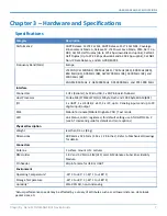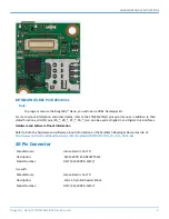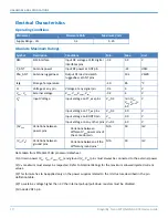
HARDWARE AND SPECIFICATIONS
Dragonfly
™
Nano MTQN-MNG3-B01 Device Guide
11
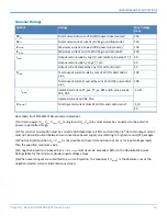
Nominal Ratings
Symbol
Ratings
Max Voltage
(mA)
Σ
IV
DD
Total current into sum of all VDD power lines (source)
1
150
Σ
IV
SS
Total current out of sum of all VSS ground lines (sink)
1
150
IV
DD(PIN)
Maximum current into each VDD power pin (source)
1
100
IV
SS(PIN)
Maximum current out of each VSS ground pin (sink)
1
100
I
IO(PIN)
Output current sunk by any I/O and control pin except FT_f
20
Output current sunk by any FT_f pin
20
Output current sourced by any I/O and control pin
20
Σ
I
IO(PIN)
Total output current sunk by sum of all I/Os and control
pins
2
100
Total output current sourced by sum of all I/Os and control
pins
2
100
I
INJ(PIN)
3
Injected current on FT_xxx, TT_xx, RST and B pins, except
PA4, PA5
-5/+0
4
Injected current on PA4, PA5
Σ
|I
INJ(PIN)
|
Total injected current (sum of all I/Os and control pins)
5
-5/0
25
Data taken from STM32L471QG processor datasheet.
(1) All main power (V
DD
, V
DDA
, V
DDIO2
, V
BAT
) and ground (V
SS
, V
SSA
) pins must always be connected to the external
power, in permitted range.
(2) This current consumption must be correctly distributed over all I/Os and control pins. The total output current
must not be sunk/sourced between two consecutive power supply pins referring to high pin count QFP packages.
(3) Positive injection (when V
IN
> V
DDIOx
) is not possible on these I/Os and does not occur for input voltages lower
than the specified maximum value.
(4) A negative injection is induced by V
IN
< V
SS. IINJ(PIN)
must never be exceeded. Refer to the Absolute Maximum
Ratings table for the minimum allowed input voltage values.
(5) When several inputs are submitted to a current injection, the maximum
Σ
|I
INJ(PIN)
| is the absolute sum of the
negative injected currents (instantaneous values).

