background image

Hardware Installation

http://www.motorola.com/computer/literature

1-25

1

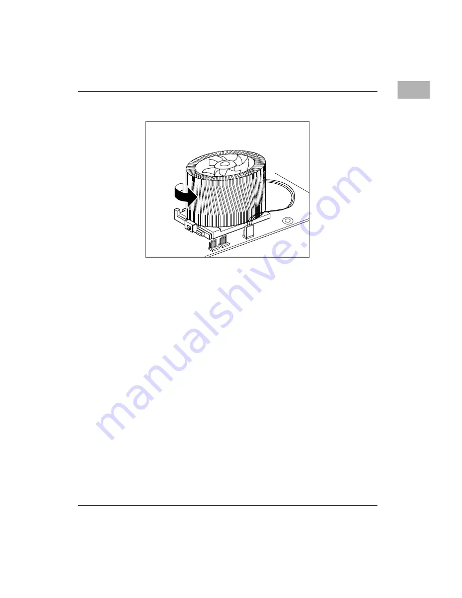
5. Twist the air cooler counter-clockwise about 1/2 inch, making sure

the spring clip features are securely seated over the socket tabs.
Verify the heat sink is firmly locked in place.

6. Plug the 3-pin connector into the 3-pin header (J18) on the

motherboard.

The air cooler is ready to work.

Connection to Peripherals

With the I/O shield in place, the PATX3070 motherboard installed in a
chassis, and modules installed on the PATX3070, you are ready to connect
peripherals and apply power to the board.

Figure 1-2 on page 1-8

shows the locations of the various cable connectors.

They are also listed in

Table 1-3 on page 1-26

with the rest of the

connectors.

For the pin assignments of the connectors listed, refer to

Chapter 4,

Connector Pin Assignments

.

b

a

Summary of Contents for PATX3070 Series

Page 1: ...PATX3070 ATX Motherboard Installation and Use PATX3070A IH1 February 2001 ...

Page 2: ... is a trademark of Lynx Real Time Systems Inc Linux is a registered trademark of Linus Torvalds Adaptec AIC and RAIDport are trademarks of Adaptec Inc which may be registered in some jurisdictions VxWorks is a registered trademark of Wind River Systems Inc SanDisk is a registered trademark and CompactFlash is a trademark of SanDisk Corporation Motorola and the stylized Motorola logo are registered...

Page 3: ...ide the Equipment Operating personnel must not remove equipment covers Only Factory Authorized Service Personnel or other qualified service personnel may remove equipment covers for internal subassembly or component replacement or any internal adjustment Service personnel should not replace components with power cable connected Under certain conditions dangerous voltages may exist even with the po...

Page 4: ...losion if battery is replaced incorrectly Replace battery only with the same or equivalent type recommended by the equipment manufacturer Dispose of used batteries according to the manufacturer s instructions Attention Il y a danger d explosion s il y a remplacement incorrect de la batterie Remplacer uniquement avec une batterie du même type ou d un type équivalent recommandé par le constructeur M...

Page 5: ...tion of Conformity is available on request Please contact your sales representative Notice While reasonable efforts have been made to assure the accuracy of this document Motorola Inc assumes no liability resulting from any omissions in this document or from the use of the information obtained therein Motorola reserves the right to revise this document and to make changes from time to time in the ...

Page 6: ...d to in writing by Motorola Inc Use duplication or disclosure by the Government is subject to restrictions as set forth in subparagraph b 3 of the Rights in Technical Data clause at DFARS 252 227 7013 Nov 1995 and of the Rights in Noncommercial Computer Software and Documentation clause at DFARS 252 227 7014 Jun 1995 Motorola Inc Computer Group 2900 South Diablo Way Tempe Arizona 85282 ...

Page 7: ...ation J9 1 9 CMOS to EEPROM Backup J27 1 10 USB Port 1 Routing J33 1 11 CMOS Battery Backup Control PIIX RTC CMOS CLR J34 1 12 Watchdog Timer Enable J43 1 13 Hardware Installation 1 13 Installation Preliminaries 1 13 PATX3070 Motherboard Installation 1 14 I O Shield 1 14 Motherboard 1 15 DIMM Memory 1 18 AGP Graphics Slot 1 19 PCI Expansion Cards 1 20 ISA Module s 1 21 SanDisk IDE CompactFlash 1 2...

Page 8: ...ssages and Beep Codes 2 6 CHAPTER 3 Features and Specifications Features 3 1 Environmental Monitoring and System Management 3 3 LM79 Hardware Monitor 3 3 CPU Temperature Monitor 3 3 AC Fail Circuit 3 4 Specifications 3 4 Cooling Requirements 3 5 CHAPTER 4 Connector Pin Assignments PATX3070 Cable Connectors 4 1 PATX3070 Socket Connectors 4 14 APPENDIX A Related Documentation Motorola Computer Group...

Page 9: ... the Motherboard 1 15 Figure 1 4 Installing the PATX3070 Motherboard in a Chassis 1 17 Figure 1 5 Installing Memory DIMM s 1 18 Figure 1 6 Installing an AGP Graphics Card 1 19 Figure 1 7 Installing PCI Module s 1 20 Figure 1 8 Installing ISA Module s 1 21 Figure 1 9 Installing a SanDisk IDE CompactFlash Card 1 22 Figure 2 1 The Basic Setup Screen 2 2 ...

Page 10: ... Table 4 9 Dual Serial Port Panel Connector J9 4 5 Table 4 10 Power Supply Fan Cable Header J10 4 5 Table 4 11 Reset Cable Header J14 4 6 Table 4 12 Chassis Fan Cable Header J15 4 6 Table 4 13 Secondary IDE Connector J16 4 6 Table 4 14 Primary IDE Connector J17 4 7 Table 4 15 CPU Fan Cable Header J18 4 8 Table 4 16 Ethernet LED Cable Header J20 J24 4 8 Table 4 17 SCSI Channel A B Connectors J19 J2...

Page 11: ...xii Table 4 28 DIMM Module Sockets U12 U15 4 18 Table 4 1 Motorola Computer Group Documents A 1 Table A 2 Manufacturers Documents A 2 Table A 3 Related Specifications A 4 ...

Page 12: ...ents Chapter 1 Hardware Preparation and Installation provides information on hardware preparation and installation for the PATX3070 Chapter 2 BIOS Self Test and Setup provides a brief description of the BIOS power on self test POST and lists the features and specifications applicable to the motherboard Chapter 3 Features and Specifications describes features and specifications of the PATX3070 Chap...

Page 13: ...r of the manual and tell how you used it Then tell us your feelings about its strengths and weaknesses and any recommendations for improvements Conventions Used in This Manual The following typographical conventions are used in this document bold is used for user input that you type just as it appears it is also used for commands options and arguments to commands and names of programs directories ...

Page 14: ...xv CR represents the carriage return or Enter key CTRL represents the Control key Execute control characters by pressing the Ctrl key and the letter simultaneously for example Ctrl d ...

Page 15: ...100 BaseTX Ethernet Interfaces single or dual population options two Ultra ATA 33 EIDE interface connectors supporting up to four hard drives CompactFlashTM Type II socket dual channel Wide Ultra SCSI interface with optional RAID support two RS 232 serial ports parallel floppy PS 2 keyboard mouse support and IrDA header watchdog interval timers hardware monitor one 2x AGP slot two 32 bit 33 MHz PC...

Page 16: ...eb Site Hardware Preparation and Installation 1 The block diagram in Figure 1 1 on page 1 3 shows the architecture of the PATX3070 motherboard Chapter 3 Features and Specifications contains complete features and specifications for the board ...

Page 17: ...t PIIX4E South Bridge BIOS Flash Watchdog MAX705 Tick Timers 2 82C54 RTC Battery ISA Slot ISA Slot CompactFlash I O Shield optional Secondary PCI Bus USB 1 USB 2 EIDE Primary EIDE Secondary 32 bit PCI Slot LM79 Monitor Programmable Power Supply HD68 82443BX North Bridge AGP Memory Controller Processor to PCI Bridge Clock Generator Reset Control AGP Slot DIMMs 168 pins 3 3V SDRAM ECC SMBus Shared S...

Page 18: ...14 Install the motherboard in the chassis Motherboard on page 1 15 Ensure that DIMM memory module s are properly installed on the motherboard DIMM Memory on page 1 18 If applicable install an AGP Graphics card on the motherboard AGP Graphics Slot on page 1 19 If applicable install any PCI expansion cards on the motherboard PCI Expansion Cards on page 1 20 If applicable install any ISA expansion ca...

Page 19: ...circuits Hardware Configuration To produce the desired configuration and ensure that the PATX3070 motherboard operates properly you may need to carry out certain hardware modifications before installing the motherboard Note that the BIOS initializes the PATX3070 motherboard Chapter 2 BIOS Self Test and Setup You may also wish to consult the PATX3070 BIOS and Programmer s Reference Guide listed in ...

Page 20: ...le Default settings are enclosed in brackets For the connector pin assignments on the PATX3070 refer to the Chapter 4 Connector Pin Assignments Note Items in brackets are factory default settings Table 1 2 PATX3070 Jumper and Switch Settings Jumper Function Settings J7 Backup Battery Selection J7 and BT1 1 2 No jumper On board battery selected External battery selected cable installed J9 CompactFl...

Page 21: ...omputer literature 1 7 1 The PATX3070 motherboard is tested and shipped with the configurations described in the following sections The PATX3070 s required and factory installed BIOS performs its power up self test POST with those factory settings ...

Page 22: ...P1 J1 J3 J37 J2 J18 U23 J30 J41 J17 J19 J21 J23 J11 U12 U13 U14 U15 J34 J27 J26 U29 Q3 Q2 1 2 1 2 1 3 2 1 10 9 1 3 A1 B1 A1 B1 A1 B2 A2 B1 A1 B2 A2 B1 A1 B2 A2 B1 A1 B2 A2 B1 A1 B2 2 1 1 3 1 4 1 11 10 20 1 2 1 2 2 1 1 50 1 4 1 3 1 26 9 10 J13 J32 U30 BTI J25 1 2 U27 1 J40 J44 1 3 J45 2 33 34 J28 A1 B2 A2 B1 J22 A1 B2 A65 B66 J15 1 3 J10 1 3 J12 1 9 2 8 T2 T1 4 3 J24 2 1 4 3 J20 J4 J5 U24 J6 1 2 ...

Page 23: ...ins 1 2 and instead connect the external battery cable to J7 Pin 1 connects to the negative side of the external battery pin 4 to the positive side CompactFlash Configuration J9 The SanDisk CompactFlash cards which can be used on the PATX3070 contain an intelligent controller for management of the Flash media The CompactFlash implementation mimics the file structure of a hard disk drive These char...

Page 24: ...ime the power on self test POST executes The factory configuration has a jumper between J27 pins 2 3 so that a fresh copy of the CMOS RAM contents is stored in EEPROM each time you power up the system If you move the jumper to J27 pins 1 2 the CMOS to EEPROM backup is disabled If the BIOS configuration data becomes corrupted while you are operating the board with the CMOS to EEPROM backup enabled ...

Page 25: ... board once more The board will reinitialize using the BIOS configuration data you have entered and a copy of the data will be placed in EEPROM USB Port 1 Routing J33 The PATX3070 is equipped with two USB Universal Serial Bus ports The primary port Port 0 is routed to a USB panel connector The secondary USB Port 1 may be directed either to a panel connector or to a connector header on the board J3...

Page 26: ...iguration has a jumper between J34 pins 2 3 enabling battery power to the CMOS RAM If you move the jumper to J34 pins 1 2 when the board is powered down the CMOS memory is cleared and BIOS default settings take over Refer also to CMOS to EEPROM Backup J27 6 2 4 8 10 To Connector J33 5 1 To Header J33 factory configuration 3 7 9 6 2 5 1 4 3 8 7 10 9 J34 Battery backup enabled 3 2 1 factory configur...

Page 27: ...otorola strongly recommends that you use an antistatic wrist strap and a conductive foam pad when installing or upgrading a system Electronic components such as disk drives computer boards and memory modules can be extremely sensitive to electrostatic discharge ESD After removing the component from its protective wrapper or from the system place the component flat on a grounded static free surface...

Page 28: ...d cable up the peripherals Proceed as described in the following sections to accomplish these tasks I O Shield The I O shield for the PATX3070 must be in place before you install the board in a chassis In most cases the I O shield is a factory installed item If you need to install the shield yourself however refer to Figure 1 3 on page 1 15 and follow the procedure below 1 Carefully remove the PAT...

Page 29: ...h other chassis the procedure may differ slightly 1 Attach an ESD strap to your wrist Attach the other end of the ESD strap to an electrical ground refer to Installation Preliminaries on page 1 13 The ESD strap must be secured to your wrist and to ground throughout the procedure 2 Ensure that the AC or DC power is switched off and remove the AC cord or DC power lines from the system Caution Insert...

Page 30: ...offs on the floor of the chassis in alignment with the PATX3070 motherboard mounting holes Use as many standoffs as feasible Caution Avoid touching areas of integrated circuitry static discharge can damage these circuits 5 Set the PATX3070 motherboard on the chassis standoffs and start the screw s provided into the standoffs without tightening them completely The chassis shown is a Motorola unit W...

Page 31: ...Hardware Installation http www motorola com computer literature 1 17 1 Figure 1 4 Installing the PATX3070 Motherboard in a Chassis 2813 0800 ...

Page 32: ...may find it more convenient to start with the inner DIMM slot and finish with the outer one In other words install DIMMs first in U15 then U14 then U13 then U12 DIMM MODULE Slots 3 through 0 Note For information on other DIMMs that may be suitable for use with this product refer to Intel s Web site listed in Appendix A Related Documentation Figure 1 5 Installing Memory DIMM s 2463 0101 ...

Page 33: ...allation http www motorola com computer literature 1 19 1 AGP Graphics Slot See Figure 1 6 below Install an AGP Accelerated Graphics Port graphics card in the AGP Slot J22 Figure 1 6 Installing an AGP Graphics Card ...

Page 34: ... first in J28 then J29 then J31 then J36 then J38 SLOT 1 SLOT 2 SLOT 3 SLOT 4 SLOT 5 Figure 1 7 Installing PCI Module s Notes Boards that occupy PCI Slot 5 and the adjacent ISA Slot J39 share I O space in the back panel If the ISA slot is occupied PCI Slot 5 must remain vacant and vice versa The two PCI slots closest to the processor are the primary PCI Slots J28 and J29 and provide a greater degr...

Page 35: ...y find it more convenient to start with the inner ISA slot and finish with the outer one In other words install the first ISA module in Slot J39 the second in Slot J41 Figure 1 8 Installing ISA Module s Note Boards that occupy ISA Slot J39 and the adjacent PCI Slot 5 J38 share I O space in the back panel If the ISA slot is occupied PCI Slot 5 must remain vacant and vice versa ...

Page 36: ...CompactFlash card installed you can store and manipulate files on the card as you would on a hard disk or floppy disk For details on installing this component refer to the SanDisk IDE FlashDrive Installation Guide at http www sandisk com cons prod_lit htm The general installation procedure is as follows see Figure 1 9 below 1 Start the CompactFlash card into the card guides on the CompactFlash con...

Page 37: ...slave mode with the other IDE device being set the opposite way If an ATAPI device is present on the bus however the CompactFlash card must be in master mode and the ATAPI device in slave mode CPU Cooler A CPU cooler is installed on the Intel PGA 370 socket to keep your microprocessor cool A CPU cooler includes a heat sink as well as a fan and is more efficient than a heat sink alone See the follo...

Page 38: ...r Web Site Hardware Preparation and Installation 1 3 Clasp the spring clip over the tab point a at the narrow end of the socket opposite CAM side of socket 4 Clasp the spring clip over the tab point b at the CAM end of the socket a b b a ...

Page 39: ...n the motherboard The air cooler is ready to work Connection to Peripherals With the I O shield in place the PATX3070 motherboard installed in a chassis and modules installed on the PATX3070 you are ready to connect peripherals and apply power to the board Figure 1 2 on page 1 8 shows the locations of the various cable connectors They are also listed in Table 1 3 on page 1 26 with the rest of the ...

Page 40: ...nector J1 bottom KB keyboard panel connector J1 top MSE mouse panel connector J3 left COM1 panel connector J3 right COM2 panel connector J4 Ethernet 1 panel connector J5 Ethernet 2 panel connector J3 top Parallel printer panel connector Board Surface Connectors J7 External battery cable header J8 Power in board connector J9 CompactFlash master slave select J10 Power supply fan cable header J12 COM...

Page 41: ...B1 Universal Serial Bus 1 header J28 PCI Slot 1 board connector J29 PCI Slot 2 board connector J30 RAIDport board connector J31 PCI Slot 3 board connector J32 LED power switch keylock speaker cable header J33 USB1 routing J34 CMOS clear J35 Infrared interface cable header J36 PCI Slot 4 board connector J37 Chassis intrusion detection cable header J38 PCI Slot 5 board connector J39 ISA Slot 1 board...

Page 42: ...y alter cooling and power requirements beyond specifications Motorola is continually improving its products to use the latest processor speeds and technologies as they become available If your application requires a different processor consult your local Motorola representative Replacing Lithium Batteries Follow these safety rules for proper battery operation and to reduce equipment and personal i...

Page 43: ... When dealing with lithium batteries carefully follow the precautions listed below in order to prevent accidents Do not short circuit Do not disassemble deform or apply excessive pressure Do not heat or incinerate Do not apply solder directly Do not use different models or new and old batteries together Do not charge Always check proper polarity Caution Danger of explosion if battery is replaced i...

Page 44: ...he ESD strap must be secured to your wrist and to ground throughout the procedure 1 To remove the battery from the module carefully pull the battery from the socket 2 Before installing a new battery ensure that the battery pins are clean 3 Note the battery polarity and press the new battery into the socket Note When the battery is in the socket no soldering is required 4 Recycle or dispose of the ...

Page 45: ...nfiguring it through the power on self test POST When these preliminaries are finished the BIOS seeks an operating system on one of the data storage devices hard drive floppy drive etc The BIOS then launches the operating system and surrenders control of system operations to it Configuration Information The system configuration information which the BIOS reads from CMOS RAM during power up has bee...

Page 46: ...p Interface The Setup utility uses a menu driven interface As shown in the following illustration each Setup screen has a menu bar a legend bar and a field specific help window For each field with predefined values an options window is available as well Figure 2 1 The Basic Setup Screen BIOS Setup Utility Main Memory Advanced Status Security Power Boot Exit Item Specific Help F1 Help Select Item C...

Page 47: ...helpful in navigating the Setup utility and configuring its functions Refer to Navigation in Setup below for details Field Help Window For most fields and submenus item specific help is displayed in a field help window on the right side of each screen The help window contains a brief description of the field or sub menu and or directions for using it Table 2 1 BIOS Setup Menus Menu Function Main S...

Page 48: ...ter again to set the selected value or press Esc to close the options widow and retain the previous setting To display a submenu use the arrow keys to move the cursor to the submenu you want a pointer marks all submenus Then press Enter To exit a submenu and return to the menu above it press Esc Pressing Esc in a principal menu such as Main or Security for example takes you directly to the Exit me...

Page 49: ...t you thoroughly understand Even seemingly small changes may cause the system to become unstable If after making and saving system changes with Setup you discover that your computer no longer is able to boot the BIOS supports an override that after five failed boot attempts boots using the BIOS defaults You should then enter Setup make any needed adjustments and save the changes Home or End Move c...

Page 50: ...fault settings without resorting to repeated boot attempts Once the defaults are restored you can restart the Setup utility and make necessary adjustments For further details on the Setup menus and the BIOS in general refer to the PATX3070 BIOS and Programmer s Reference Guide listed in Appendix A Related Documentation BIOS Messages and Beep Codes During POST the BIOS may display status error mess...

Page 51: ...lists the features of the PATX3070 motherboard Table 3 1 PATX3070 Motherboard Features Summary Feature Description Processor Single Intel PGA370 Pentium III or Celeron processor with auto selection of bus frequency and core voltages 66 100 MHz front side bus FSB frequency L2 Cache 256KB on die Advanced Transfer Cache ATC 128KB ATC for the Celeron Processor DRAM Four 168 pin DIMM sockets 3 3V I2 C ...

Page 52: ...ry backed RAM available for BIOS EEPROM backup for CMOS RAM Form Factor Standard ATX 9 6 inches by 12 inches Interrupt Controllers Intel 82371EB PIIX4E 82C59 compatible PCI Interface 5V 32 bit interface at up to 33 MHz 5 PCI expansion slots 3 of which are optional and are expanded across the PCI to PCI bridge DEC21152 ISA Interface 82371EB PCI to ISA IDE Xcelerator PIIX4E Two ISA expansion slots o...

Page 53: ...agement interrupts as appropriate for your application SMI signals from the LM79 are routed to the PIIX4E s EXTSMI input The PATX3070 also includes circuitry for the detection of chassis intrusion events When implemented with appropriate sensory devices in an enclosure the intrusion detection circuitry is active continually even while the system is shut down as long as backup battery or standby po...

Page 54: ...ions for the PATX3070 motherboard Table 3 2 PATX3070 Motherboard Specifications Characteristics Specifications Power Requirements exclusive of attached daughter boards and or peripherals One PGA370 socket supports either a 300 MHz Celeron processor or a 600 MHz Pentium III processor 5VDC 5 5A typical 15 8A maximum 3 3VDC 5 4A typical 12 7A maximum 12VDC 5 0 3A typical 0 5A maximum 12VDC 5 0 05A ty...

Page 55: ... two RJ 45 connectors 10 100 Mbps interface speed Serial port interface asynchronous 9 pin D sub panel I O Parallel port interface 25 pin D sub panel I O Mouse interface 6 pin mini DIN panel I O Keyboard interface 6 pin mini DIN panel I O USB Dual independent USB channels for 1 5Mbps and 12Mbps transfer rates allow for easy hot plugging of USB peripherals Super I O device National PC97317 controll...

Page 56: ...I cards and ISA cards The PATX3070 provides headers J10 J15 to power these fans if necessary While the exact amount of airflow required for cooling depends on the ambient air temperature enclosure venting and the type number and location of expansion modules and other heat sources an average airflow of 40 CFM cubic feet minute should provide adequate cooling for most applications ...

Page 57: ...therboard For device socket pin assignments refer to PATX3070 Socket Connectors on page 4 14 Table 4 1 Keyboard Mouse Panel Connector J1 1 KBDAT_FB Keyboard Interface Bottom 2 3 CH_GND 4 KB5V_FB 5 KBCLK_FB 6 7 MSDAT_FB Mouse Interface Top 8 9 CH_GND 10 KB5V_FB 11 MSCLK_FB 12 Table 4 2 Dual USB Panel Connector J2 L1 USBV0 USB Port 0 Bottom L2 USBP0 L3 USBP0 L4 USBG0 ...

Page 58: ...or J3 1 SP_DCD1 SP_DSR1 2 3 SP_RXD1 SP_RTS1 4 5 SP_TXD1 SP_CTS1 6 7 SP_DTR1 SP_RI1 8 9 GND Key 10 Table 4 4 Parallel Printer Panel Connector J3 top 1 STB AFD 14 2 PD0 ERR 15 3 PD1 INIT 16 4 PD2 SLIN 17 5 PD3 GND 18 6 PD4 GND 19 7 PD5 GND 20 8 PD6 GND 21 9 PD7 GND 22 10 ACK GND 23 11 BUSY GND 24 12 PE GND 25 13 SLCT Table 4 2 Dual USB Panel Connector J2 Continued ...

Page 59: ... 3 4 Table 4 5 Ethernet 1 Panel Connector J4 1 TX1 2 TX1 3 RX1 4 TC2RR1 5 TC2RR1 6 RX1 7 TC2RR 8 TC2RR Table 4 6 Ethernet 2 Panel Connector J5 1 TX2 2 TX2 3 RX2 4 TC2RR2 5 TC2RR2 6 RX2 7 TC2RR 8 TC2RR Table 4 7 External Battery Cable Header J7 1 GND 2 BAT_G 3 Key 4 VBAT ...

Page 60: ...erature Center Web Site Connector Pin Assignments 4 Table 4 8 POWER IN Connector J8 1 3 3V 3 3V 11 2 3 3V 12V 12 3 GND GND 13 4 5V PS_ON 14 5 GND GND 15 6 5V GND 16 7 GND GND 17 8 POWER_GOOD 5V 18 9 5VSTB 5V 19 10 12V 5V 20 ...

Page 61: ...nector J9 P1 SP_DCD0 COM1 Serial Port Bottom P2 SP_RXD0 P3 SP_TXD0 P4 SP_DTR0 P5 GND P6 SP_DSR0 P7 SP_RTS0 P8 SP_CTS0 P9 SP_RI0 Q1 SP_DCD1 COM2 Serial Port Top Q2 SP_RXD1 Q3 SP_TXD1 Q4 SP_DTR1 Q5 GND Q6 SP_DSR1 Q7 SP_RTS1 Q8 SP_CTS1 Q9 SP_RI1 Table 4 10 Power Supply Fan Cable Header J10 1 GND 2 12 0V 3 FANTACH2 ...

Page 62: ...J15 1 GND 2 12 0V 3 FANTACH1 Table 4 13 Secondary IDE Connector J16 1 IDERSTS GND 2 3 DDS7R DDS8R 4 5 DDS6R DDS9R 6 7 DDS5R DDS10R 8 9 DDS4R DDS11R 10 11 DDS3R DDS12R 12 13 DDS2R DDS13R 14 15 DDS1R DDS14R 16 17 DDS0R DDS15R 18 19 GND Key 20 21 IDEDRQ1R GND 22 23 IDEIOW1 R GND 24 25 IDEIOR1 R GND 26 27 IDEIORDY1R IDESELB 28 29 IDEDACK1 R GND 30 31 IDEIRQ1R 32 ...

Page 63: ...GND 2 3 PDD7R PDD8R 4 5 PDD6R PDD9R 6 7 PDD5R PDD10R 8 9 PDD4R PDD11R 10 11 PDD3R PDD12R 12 13 PDD2R PDD13R 14 15 PDD1R PDD14R 16 17 PDD0R PDD15R 18 19 GND Key 20 21 IDEDRQ0R GND 22 23 IDEIOW0 R GND 24 25 IDEIOR0 R GND 26 27 IDEIORDY0R IDESELA 28 29 IDEDACK0 R GND 30 31 IDEIRQ0R 32 33 PDA1R 34 35 PDA0R PDA2R 36 37 IDECS01 R IDECS03 R 38 39 HDACTA GND 40 Table 4 13 Secondary IDE Connector J16 Conti...

Page 64: ...ader J20 J24 1 100Mbit LED 10Mbit LED 100Mbit LED 10Mbit LED 2 3 Activity LED Activity LED 4 Table 4 17 SCSI Channel A B Connectors J19 J21 1 GND GND 2 3 GND GND 4 5 GND GND 6 7 GND GND 8 9 GND GND 10 11 GND GND 12 13 GND GND 14 15 GND GND 16 17 5 0V TERMPWR 5 0V TERMPWR 18 19 No Connection GND 20 21 GND GND 22 23 GND GND 24 25 GND GND 26 27 GND GND 28 29 GND GND 30 ...

Page 65: ...CDPL 48 49 GND GND 50 51 5 0V TERMPWR 5 0V TERMPWR 52 53 No Connection GND 54 55 SATN GND 56 57 SBSY SACK 58 59 SRST SMSG 60 61 SSEL SCD 62 63 SREQ SIO 64 65 SCDB 8 SCDB 9 66 67 SCDB 10 SCDB 11 68 Table 4 18 Floppy Disk Drive Connector Header J23 1 GND FLPREDWC 2 3 GND 4 5 KEY FLPDRATE0 6 7 GND FLPINDEX 8 9 GND FLPMOTEA 10 11 GND FLPDRVSB 12 13 GND FLPDRVSA 14 15 GND FLPMOTEB 16 Table 4 17 SCSI Ch...

Page 66: ...9 USB 1 Cable Header J26 1 USBV1 I 2 USBP1 I 3 USBV1 I 4 USBG1I Table 4 20 RAIDport Connector Header J30 Row A Row B 1 No Connection No Connection 1 2 No Connection No Connection 2 3 No Connection GND 3 4 No Connection 4 5 EXTARBACK EXTARBREQ 5 6 No Connection No Connection 6 7 No Connection No Connection 7 8 No Connection No Connection 8 9 IDDAT SCSILED 9 10 No Connection No Connection 10 Table 4...

Page 67: ... US_RAMPS US_MD 4 18 19 US_MD 3 GND 19 20 US_MD 5 US_MD 6 20 21 US_MA 13 US_MA 14 21 22 US_MD 7 US_MA 12 22 23 US_MA 11 US_MA 10 23 24 US_MA 9 US_MA 8 24 25 US_MA 7 ARO_PRSNT 25 26 GND US_MA 6 26 27 US_MA 5 US_MA 4 27 28 US_MA 3 GND 28 29 US_SEECS US_MA 2 29 30 US_MA 1 US_MA 0 30 Table 4 21 LED Power Switch Keylock Speaker Header J32 1 GND 2 SUSPLED 3 PLED 4 No Connection 5 6 No Connection 7 Table...

Page 68: ...11 12 HDLED 13 14 HARDDRV 15 HDLED 16 17 GND 18 19 PLED 20 21 KBLOCK 22 GND 23 No Connection 24 SPK_P 25 No Connection 26 SPK_N Table 4 22 Infrared Interface Cable Header J35 1 5V IRSL1 2 3 IRSL0 GND 4 5 IRRXD IRSL2 6 7 GND ID3 8 9 IRTXD GND 10 Table 4 21 LED Power Switch Keylock Speaker Header J32 Continued ...

Page 69: ...PATX3070 Cable Connectors http www motorola com computer literature 4 13 4 Table 4 23 Chassis Intrusion Detection Cable Header J37 1 2 CHASINTV 3 CHAS_INT ...

Page 70: ...ND 8 9 GND GND 10 11 GND GND 12 13 5 0V GND 14 15 GND GND 16 17 GND SDA2R 18 19 SDA1R SDA0R 20 21 DDS0R DDS1R 22 23 DDS2R CF_IOCS16 24 25 CD2 CD1 26 27 DDS11R DDS12R 28 29 DDS13R DDS14R 30 31 DDS15R IDECS3 R 32 33 CF_VS1 IDEIOR1 R 34 35 IDEIOW1 R CF_WE 36 37 IDEIRQ1R 5 0V 38 39 CF_CSEL CF_VS2 40 41 IDERSTS R IDEIORDY1R 42 43 CF_INPACK CF_REG 44 45 DASP SPDIAG 46 47 DDS8R DDS9R 48 49 DDS10R GND 50 ...

Page 71: ..._STB 18 19 GROUND GSBA5 20 19 GROUND GSBA4 20 21 GSBA7 22 21 GSBA6 22 23 24 23 24 25 GAD30 26 25 GAD31 26 27 GAD28 3 3V 28 27 GAD29 3 3V 28 29 GAD26 GAD24 30 29 GAD27 GAD25 30 31 GROUND Reserved 32 31 GROUND GAD_STB 1 32 33 GCBE3 3 3V 34 33 GAD23 3 3V 34 35 GAD22 GAD20 36 35 GAD21 GAD19 36 37 GROUND GAD18 38 37 GROUND GAD17 38 39 GAD16 3 3V 40 39 GCBE 2 3 3V 40 41 GFRAME Reserved 42 41 GIRDY Reser...

Page 72: ...6 5 5V 5V 6 7 INTC 5V 8 7 INTB INTD 8 9 RESERVED 5V 10 9 PCI0 RESERVED 10 11 RESERVED GROUND 12 11 PCI1 GROUND 12 13 GROUND RESERVED 14 13 GROUND RESERVED 14 15 PCIRESET 5V 16 15 GROUND PCLK 16 17 PGNT GROUND 18 17 GROUND PREQ 18 19 PME AD30 20 19 5V AD31 20 21 3 3V AD28 22 21 AD29 GROUND 22 23 AD26 GROUND 24 23 AD27 AD25 24 25 AD24 IDSEL 26 25 3 3V CBE 3 26 27 3 3V AD22 28 27 AD23 GROUND 28 29 AD...

Page 73: ...01 58 59 5V REQ64S0 60 59 5V ACK64S0 60 61 5V 5V 62 61 5V 5V 62 Table 4 27 ISA Connectors J39 41 Row A Row B Row C Row D 1 IOCHK GROUND SBHE MEMCS16 1 2 SD7 RSTIS LA23 IOCS16 2 3 SD6 5V LA22 IRQ10 3 4 SD5 IRQ9 LA21 IRQ11 4 5 SD4 5V LA20 IRQ12 5 6 SD3 DRQ2 LA19 IRQ15 6 7 SD2 12V LA18 IRQ14 7 8 SD1 ZWS LA17 DACK0 8 9 SD0 12V MEMR DRQ0 9 10 IOCHRDY GROUND MEMW DACK5 10 11 AEN SMEMW SD8 DRQ5 11 12 SA1...

Page 74: ...28 SA3 BALE 29 SA2 5V 30 SA1 OSC 31 SA0 GROUND Table 4 28 DIMM Module Sockets U12 U15 Pin Signal 1 Vss 22 CB1 43 Vss 64 Vss 2 DQ0 23 Vss 44 DU12 65 DQ21 3 DQ1 24 No Connection 45 CS2 66 DQ22 4 DQ2 25 No Connection 46 DQM2 67 DQ23 5 DQ3 26 Vcc 47 DQM3 68 Vss 6 Vcc 27 WE 48 No Connection 69 DQ24 7 DQ4 28 DQM0 49 Vcc 70 DQ25 8 DQ5 29 DQM1 50 No Connection 71 DQ26 9 DQ6 30 CS0 51 No Connection 72 DQ27...

Page 75: ...127 Vss 148 Vss 86 DQ32 107 Vss 128 CKE0 149 DQ53 87 DQ33 108 No Connection 129 CS3 150 DQ54 88 DQ34 109 No Connection 130 DQM6 151 DQ55 89 DQ35 110 Vcc 131 DQM7 152 Vss 90 Vcc 111 CAS 132 VSS 153 DQ56 91 DQ36 112 DQM4 133 Vcc 154 DQ57 92 DQ37 113 DQM5 134 No Connection 155 DQ58 93 DQ38 114 CS1 135 No Connection 156 DQ59 94 DQ39 115 RAS 136 CB6 157 Vcc 95 DQ40 116 Vss 137 CB7 158 DQ60 96 Vss 117 A...

Page 76: ...Web Site Connector Pin Assignments 4 102 Vcc 123 A13 144 DQ52 165 SA0 103 DQ46 124 Vcc 145 No Connection 166 SA1 104 DQ47 125 CLK1 146 No Connection 167 SA2 105 CB4 126 DU1 147 DOREGE 168 Vcc Table 4 28 DIMM Module Sockets U12 U15 Continued ...

Page 77: ... To obtain the most up to date product information in PDF or HTML format visit http www motorola com computer literature Manufacturers Documents For additional information refer to the following table for manufacturers data sheets or user s manuals As an additional help a source for the listed document is provided Please note that while these sources have been verified the information is subject t...

Page 78: ...e Intel Corporation http developer intel com design chipsets datashts 290562 htm 29056201 pdf Intel 82559ER Fast Ethernet PCI Bus Controller with Integrated PHY External Design Specification Intel Corporation http developer intel com design network datashts 738259 htm 73825902 pdf 82C54 CMOS Programmable Interval Timer Data Sheet Intersil Corporation http www intersil com search FN2970 pdf AIC 789...

Page 79: ...I2 C Multiplexer Philips Semiconductor http www semiconductors com acrobat datasheets PCA8550_3 pdf PCA8550_2 pdf SanDisk CompactFlash cartridge SanDisk Corporation http www sandisk com cons prod_lit htm CompactFlash Product Data Smart 5 Boot Block Flash Memory Family 2 4 8 Mbit Specification Intel Corporation http developer intel com design flcomp PRODBREF 297810 htm 297810 htm Table A 2 Manufact...

Page 80: ...ectrical and Electronics Engineers Inc http standards ieee org catalog IEEE Standard 1284 Peripheral Component Interconnect PCI Local Bus Specification Revision 2 0 PCI Special Interest Group http www pcisig com PCI Local Bus Specification Information Technology Local and Metropolitan Networks Part 3 Carrier Sense Multiple Access with Collision Detection CSMA CD Access Method and Physical Layer Sp...

Page 81: ...CI Open Host Controller Interface Spec for USB Compaq Corporation Microsoft Corporation National Semiconductor http www3 compaq com support http www national com http www microsoft com Open HCI Release 1 0 12 15 95 Accelerated Graphics Port Interface Specification Revision 1 0 Intel Corporation http www intel com technology agp agp_index htm agp10 pdf Universal Host Controller Interface UHCI Desig...

Page 82: ...3 1 H hardware monitor 3 3 I installation AGP module 1 19 battery replacement 1 28 cpu cooler 1 23 I O shield 1 14 ISA module s 1 21 memory modules 1 18 PATX3000 motherboard 1 15 PCI module s 1 20 processor 1 28 SanDisk IDE CompactFlash card 1 22 J jumpers J13 CompactFlash configuration 1 9 1 23 J32 CMOS to EEPROM backup con figuration 1 10 J42 second USB routing 1 11 J44 CMOS battery backup contr...

Page 83: ...20 R reconfiguring the BIOS 1 10 related specifications A 4 S setting jumpers and switches 1 7 shared PCI ISA slot 1 20 specifications PATX3000 motherboard 3 4 specifications related A 4 system management features 3 3 system startup overview 1 4 T temperature monitor CPU 3 3 U URLs uniform resource locators A 5 ...

Reviews: