background image

Registers

http://www.motorola.com/computer/literature

2-101

2

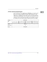
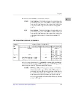
Revision ID/ Class Code Registers

REVID

Revision ID. This register identifies the PHB revision 
level. This register is duplicated in the PPC Registers.

CLASS

Class Code. This register identifies PHB as the following:

Base Class Code

$06

PCI Bridge Device

Subclass Code

$00

PCI Host Bridge

Program Class Code

$00

Not Used

Header Type Register

The Header Type Register (Header) identifies the PHB as the following:

Header Type: $00 - Single Function Configuration Header

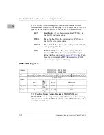
Offset

$08

Bit

3
1

3
0

2
9

2
8

2
7

2
6

2
5

2
4

2
3

2
2

2
1

2
0

1
9

1
8

1
7

1
6

1
5

1
4

1
3

1
2

1
1

1
0 9 8 7 6 5 4 3 2 1 0

Name

CLASS

REVID

Operation

R

R

Reset

$060000

$01

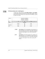
Offset

$0C

Bit

31

30

29

28

27

26

25

24

23

22

21

20

19

18

17

16

15

14

13

12

11

10

9

8

7

6

5

4

3

2

1

0

Name

HEADER

Operation

R

R

R

R

Reset

$00

$00

$00

$00

Summary of Contents for MVME5100 Series

Page 1: ...MVME5100 Single Board Computer Programmer s Reference Guide V5100A PG2 September 2001 Edition ...

Page 2: ...trademark of Motorola Inc PowerPC and the PowerPC logo are registered trademarks and PowerPC 750 is a trademark of International Business Machines Corporation and are used by Motorola Inc under license from International Business Machines Corporation All other products mentioned in this document are trademarks or registered trademarks of their respective holders ...

Page 3: ...ide the Equipment Operating personnel must not remove equipment covers Only Factory Authorized Service Personnel or other qualified service personnel may remove equipment covers for internal subassembly or component replacement or any internal adjustment Service personnel should not replace components with power cable connected Under certain conditions dangerous voltages may exist even with the po...

Page 4: ...losion if battery is replaced incorrectly Replace battery only with the same or equivalent type recommended by the equipment manufacturer Dispose of used batteries according to the manufacturer s instructions Attention Il y a danger d explosion s il y a remplacement incorrect de la batterie Remplacer uniquement avec une batterie du même type ou d un type équivalent recommandé par le constructeur M...

Page 5: ...rts have been made to assure the accuracy of this document Motorola Inc assumes no liability resulting from any omissions in this document or from the use of the information obtained therein Motorola reserves the right to revise this document and to make changes from time to time in the content hereof without obligation of Motorola to notify any person of such revision or changes Electronic versio...

Page 6: ...d to in writing by Motorola Inc Use duplication or disclosure by the Government is subject to restrictions as set forth in subparagraph b 3 of the Rights in Technical Data clause at DFARS 252 227 7013 Nov 1995 and of the Rights in Noncommercial Computer Software and Documentation clause at DFARS 252 227 7014 Jun 1995 Motorola Inc Computer Group 2900 South Diablo Way Tempe Arizona 85282 ...

Page 7: ... 7 PCI Local Bus Memory Map 1 8 VMEbus Memory Map 1 8 System Bus 1 8 Processors 1 9 Processor Type Identification 1 9 Processor PLL Configuration 1 9 L2 Cache 1 9 L2 Cache SRAM Size 1 10 Cache Speed 1 10 FLASH Memory 1 10 ECC Memory 1 11 P2 I O Modes 1 11 Serial Presence Detect SPD Definitions 1 12 Hawk ASIC 1 12 Hawk I2C interface and configuration information 1 13 Vital Product Data VPD and Seri...

Page 8: ... Features Register 1 1 31 Board Last Reset Register 1 32 Extended Features Register 2 1 33 CHAPTER 2 Hawk PCI Host Bridge Multi Processor Interrupt Controller Introduction 2 1 Overview 2 1 Features 2 1 Block Diagram 2 3 Functional Description 2 4 Architectural Overview 2 4 PPC Bus Interface 2 5 PPC Address Mapping 2 6 PPC Slave 2 7 PPC FIFO 2 9 PPC Master 2 10 PPC Arbiter 2 15 PPC Parity 2 17 PPC ...

Page 9: ...Interrupts IPI 2 55 8259 Compatibility 2 55 Hawk Internal Errror Interrupt 2 55 Timers 2 56 Interrupt Delivery Modes 2 56 Block Diagram Description 2 57 Program Visible Registers 2 59 Interrupt Pending Register IPR 2 59 Interrupt Selector IS 2 59 Interrupt Request Register IRR 2 60 In Service Register ISR 2 60 Interrupt Router 2 60 Programming Notes 2 62 External Interrupt Service 2 62 Reset State...

Page 10: ...neral Purpose Registers 2 96 PCI Registers 2 97 Vendor ID Device ID Registers 2 98 PCI Command Status Registers 2 99 Revision ID Class Code Registers 2 101 Header Type Register 2 101 MPIC I O Base Address Register 2 102 MPIC Memory Base Address Register 2 102 PCI Slave Address 0 1 2 and 3 Registers 2 103 PCI Slave Attribute Offset 0 1 2 and 3 Registers 2 104 CONFIG_ADDRESS Register 2 106 CONFIG_DA...

Page 11: ...1 Bit Ordering Convention 3 1 Features 3 1 Block Diagrams 3 2 Functional Description 3 6 SDRAM Accesses 3 6 Four beat Reads Writes 3 6 Single beat Reads Writes 3 6 Address Pipelining 3 6 Page Holding 3 7 SDRAM Speeds 3 7 SDRAM Organization 3 9 PPC60x Bus Interface 3 9 Responding to Address Transfers 3 9 Completing Data Transfers 3 9 PPC60x Data Parity 3 10 PPC60x Address Parity 3 10 Cache Coherenc...

Page 12: ...h Register 3 51 Scrub Address Register 3 52 ROM A Base Size Register 3 53 ROM B Base Size Register 3 56 ROM Speed Attributes Registers 3 58 Data Parity Error Log Register 3 60 Data Parity Error Address Register 3 61 Data Parity Error Upper Data Register 3 61 Data Parity Error Lower Data Register 3 62 I2C Clock Prescaler Register 3 63 I2C Control Register 3 63 I2C Status Register 3 64 I2C Transmitt...

Page 13: ...s 4 1 8259 Interrupts 4 3 Exceptions 4 5 Sources of Reset 4 5 Soft Reset 4 5 CPU Reset 4 5 Error Notification and Handling 4 6 Endian Issues 4 7 Processor Memory Domain 4 9 MPIC s Involvement 4 9 PCI Domain 4 9 APPENDIX A Related Documentation Motorola Computer Group Documents A 1 Manufacturers Documents A 2 Related Specifications A 4 APPENDIX B MVME5100 VPD Reference Information Vital Product Dat...

Page 14: ...tions Product Configuration Options Data B 7 VPD Definitions FLASH Memory Configuration Data B 9 VPD Definitions L2 Cache Configuration Data B 10 VPD Definitions VPD Revision Data B 12 Configuration Checksum Calculation Code B 14 Serial Presence Detect SPD Checksum Calculation B 15 ...

Page 15: ...ock Diagram 2 58 Figure 3 1 Hawk Used with Synchronous DRAM in a System 3 2 Figure 3 2 Hawk s System Memory Controller Internal Data Paths 3 3 Figure 3 3 Overall SDRAM Connections 4 Blocks using Register Buffers 3 4 Figure 3 4 Hawk s System Memory Controller Block Diagram 3 5 Figure 3 5 Programming Sequence for I2C Byte Write 3 24 Figure 3 6 Programming Sequence for I2C Random Read 3 26 Figure 3 7...

Page 16: ...xvi ...

Page 17: ...xtended Features Register 1 1 31 Table 1 17 Extended Features Register 2 1 33 Table 2 1 PPC Slave Response Command Types 2 8 Table 2 2 PPC Master Transaction Profiles and Starting Offsets 2 11 Table 2 3 PPC Master Write Posting Options 2 12 Table 2 4 PPC Master Read Ahead Options 2 12 Table 2 5 PPC Master Transfer Types 2 14 Table 2 6 PPC Arbiter Pin Assignments 2 15 Table 2 7 PCI Slave Response C...

Page 18: ...able 3 9 Register Summary 3 36 Table 3 10 Block_A B C D E F G H Configurations 3 42 Table 3 11 ROM Block A Size Encoding 3 54 Table 3 12 rom_a_rv and rom_b_rv encoding 3 54 Table 3 13 Read Write to ROM Flash 3 55 Table 3 14 ROM Block B Size Encoding 3 57 Table 3 15 ROM Speed Bit Encodings 3 59 Table 3 16 Trc Encoding 3 69 Table 3 17 tras Encoding 3 69 Table 3 18 Deriving tras trp trcd and trc Cont...

Page 19: ...Specifications A 4 Table B 1 VPD Packet Types B 4 Table B 2 MCG Product Configuration Options Data B 7 Table B 3 FLASH Memory Configuration Data B 9 Table B 4 L2 Cache Configuration Data B 10 Table B 5 VPD Revision Data B 12 ...

Page 20: ...xx ...

Page 21: ...ote that much of the board s programming functionality is associated with the Hawk ASIC Additional programming information can also be found in the following manuals refer to Appendix A Related Documentation PPCBug Firmware Package User s Manual PPCBug Diagnostics Manual MPC750 RISC Microprocessor User s Manual MPC7400 RISC Microprocessor User s Manual Universe II User Manual The MVME5100 is a hig...

Page 22: ... MPC7400 and 17MB Flash MVME5101 0131 64MB ECC SDRAM SCANBE handles 1MB L2 Cache MVME5101 0161 512MB ECC SDRAM SCANBE handles 1MB L2 Cache MVME5101 0133 64MB ECC SDRAM IEEE 1101 handles 1MB L2 Cache MVME5101 0163 512MB ECC SDRAM IEEE 1101 handles 1MB L2 Cache MVME5101 2131 64MB ECC SDRAM SCANBE handles 2MB L2 Cache MVME5101 2133 64MB ECC SDRAM IEEE 1101 handles 2MB L2 Cache MVME5101 2141 128MB ECC...

Page 23: ...ansition module Two DB 9 async serial port connectors two HD 26 sync async serial port connectors one HD 36 parallel port connector one RJ 45 10 100 Ethernet connector includes 3 row DIN P2 adapter module and cable for 8 bit SCSI MVME761 011 Transition module Two DB 9 async serial port connectors two HD 26 sync async serial port connectors one HD 36 parallel port connector and one RJ 45 10 100 Eth...

Page 24: ...s for either two single wide or one double wide PMC cards optional PMCSPAN 010 PMCSPAN 010 Secondary 32 bit PCI expansion plugs directly into PMCSPAN 002 providing two additional PMC slots RAM500 004 Stackable top 64MB ECC SDRAM mezzanine RAM500 006 Stackable top 256MB ECC SDRAM mezzanine RAM500 016 Stackable bottom 256MB ECC SDRAM mezzanine Date Doc Rev Changes 09 2001 V5100A PG2 Memory Maps and ...

Page 25: ... including a listing of the Hawk MPIC External Interrupts the 8259 Interrupts and a description of certain exceptions such as sources of reset error notification and handling endian issues and processor Hawk relationships Appendix A Related Documentation provides a listing of related Motorola manuals vendor documentation and industry specifications Appendix B MVME5100 VPD Reference Information pro...

Page 26: ...ands and names of programs directories and files italic is used for names of variables to which you assign values Italic is also used for comments in screen displays and examples and to introduce new terms courier is used for system output for example screen displays reports examples and system prompts Enter Return or CR CR represents the carriage return or Enter key CTRL represents the Control ke...

Page 27: ...sertion and assert refer to a signal that is active or true negation and negate indicate a signal that is inactive or false These terms are used independently of the voltage level high or low that they represent Data and address sizes are defined as follows Specifies a binary number Specifies a decimal number Byte 8 bits numbered 0 through 7 with bit 0 being the least significant Half word 16 bits...

Page 28: ...xxviii ...

Page 29: ...the PCI bus It provides 32 bit addressing and 64 bit data however 64 bit addressing dual address cycle is not supported The ASIC also supports various processor external bus frequencies up to 100 MHz Note Unless otherwise specified the designation MVME5100 refers to all models of the MVME5100 series Single Board Computers The following table lists the key features of the MVME5100 Table 1 1 MVME Ke...

Page 30: ...Routed to the Front Panel RJ 45 Connnector COM1 and On Board Header COM2 Dual Ethernet Interfaces one routed to the Front Panel RJ 45 one routed to the Front Panel RJ 45 or optionally routed to P2 RJ 45 on MVME761 VMEbus Tundra Universe Controller 64 bit PCI Programmable Interrupter Interrupt Handler Programmable DMA Controller With Link List Support Full System Controller Functions PCI PMC Expans...

Page 31: ...H 1MB to 17MB Clock Generator VME Bridge Universe 2 Ethernet 1 10 100TX Buffers RTC NVRAM WD M48T37V TL16C550 UART 9pin Front Panel VME P2 RJ45 PMC Front I O PMC Front I O SLot1 Slot2 2 64 bit PMC Slots L2 Cache 1M 2M Ethernet 2 10 100TX 10 100Tx RJ45 10 100Tx Hawk X bus RJ45 DEBUG planar 761 or PMC IPMC761 RECEPTACLE Mezzanine SDRAM 32MB to 512MB SDRAM 32MB to 512MB HDR Hawk Asic System Memory Co...

Page 32: ... the processor is identical to the CHRP memory map described in this document The MVME5100 is fully capable of supporting both the PREP and the CHRP processor memory maps with ROM FLASH size limited to 16MB and RAM size limited to 2GB Default Processor Memory Map The default processor memory map that is valid at power up or reset remains in effect until reprogrammed for specific applications Table...

Page 33: ...emory Map The following table describes a suggested CHRP Memory Map from the point of view of the processor This memory map is an alternative to the PREP memory map Note in all recommended CHRP maps the beginning of PCI Memory Space is determined by the end of DRAM rounded up to the nearest 256MB boundry as required by CHRP For example if memory was 1G on the baseboard and 192MB on a mezzanine the...

Page 34: ...emory space Table 1 3 Suggested CHRP Memory Map Processor Address Size Definition Notes Start End 0000 0000 top_dram dram_size System Memory onboard DRAM 1 top_dram F3FF FFFF 4G dram_size PCI Memory Space 1 5 F400 0000 F7FF FFFF 64MB FLASH Bank A optional 1 2 F800 0000 FBFF FFFF 64MB FLASH Bank B optional 1 2 FC00 0000 FDFF FFFF 32MB Reserved FE00 0000 FE7F FFFF 8MB PCI ISA I O Space 1 FE80 0000 F...

Page 35: ...ME5100 Single Board Computer Installation and Use manual VME Memory Map The MVME5100 is fully capable of supporting both the PREP and the CHRP VME Memory Maps with RAM size limited to 2GB The default values for the VME Slave Image registers are listed in Chapter 3 PPCBug of the MVME5100 Single Board Computer Installation and Use manual Table 1 4 Hawk PPC Register Values for Suggested Memory Map Ad...

Page 36: ...patible memory maps refer to the Hawk portion of this manual Chapters 2 and 3 VMEbus Memory Map The map of the VMEbus is programmable Like other parts of the MVME510x memory map the mapping of local resources as viewed by VMEbus masters varies among applications The Universe PCI VME bus bridge ASIC includes a user programmable map decoder for the VMEbus to local bus interface The address translati...

Page 37: ...vels use the same nomenclature as the MPC750 e g 0x0100 and so on Processor PLL Configuration The processor internal clock frequency core frequency is a multiple of the system bus frequency The processor has four configuration pins PLL_CFG 0 3 for hardware strapping of the processor core frequency between 2x and 8x the system bus frequency in 0 5x steps The PLL configuration is dynamic at power up...

Page 38: ...3 in 5 steps The core to cache ratio is selected by reading the VPD SROM and programming the L2CLK bits of the processor s Cache Control Register Refer to the MPC7400 RISC Microprocessor Users Manual or the MPC750 RISC Microprocessor Users Manual as listed in Appendix A Related Documentation for more information FLASH Memory The MVME5100 contains two banks of FLASH memory Bank B consists of two 32...

Page 39: ...ated the planar memory blocks appear as Block A and Block B to the Hawk The optional mezzanine memory blocks appear as Block C and Block E to the Hawk The optional memory mezzanine can configure the planar local bus frequency upon power up This will reduce the planar local bus frequency of 100 MHz to 83 33 MHz when mezzanines are used Either one or two mezzanines can be installed Each mezzanine wi...

Page 40: ...itions The MVME5100 SPD uses the SPD JEDEC standard definition On board SPD for SDRAM Bank A or both A and B of the Hawk is accessed at Address A8 Only Bank A or Banks A and B may be populated If both Banks A and B are populated they will be of the same speed and memory size Memory Mezzanine 1 SPD for SDRAM Bank C of the Hawk is accessed at Address AA Memory Mezzanine 2 SPD for SDRAM Bank E of the...

Page 41: ...d to maintain the configuration information related to the board Vital Product Data VPD User Configuration Data UCD and a separate EEPROM for on board Memory Subsystem Data MSD If an optional memory mezzanine is used that mezzanine shall contain a separate EEPROM with its own memory subsystem data Each slave device connected to the I2 C bus is software addressable by a unique address There can be ...

Page 42: ...formation on the VPD and SPD data formats and defintions refer to Appendix B MVME5100 VPD Reference Information The registers related to this information is accessed through the I2 C interface of the Hawk ASIC Table 1 5 I2C Device Addressing Device Function Size Device Address A2A1A0 Software Address Onboard Configuration VPD 256x8 000b A0 Onboard User Configuration Data UPD 256x8 001b A2 IPMC761 ...

Page 43: ...I mezzanine card PCI Expansion Slot PCI Arbitration Assignments for Hawk ASIC The PCI arbitration is performed by the Hawk ASIC which supports seven external PCI masters in addition to itself Details on PCI arbitration can be found futher on in this chapter PCI Arbitration Assignments for Hawk ASIC The arbitration assignments for the MVME510x are shown in the following table Table 1 6 PCI Arbitrat...

Page 44: ... Station Address corresponds to Port 1 and the lower Ethernet Station Address corresponds to Port 2 The Ethernet Station Addresses are displayed on labels attached to the PMC front panel keep out area In addition the presence of the Ethernet device can be positively determined by reading the Vital Product Data VPD Serial EEPROM which provides storage of the MVME5100 hardware configuration Refer to...

Page 45: ...ase Module Feature Register The INTA INTB INTC and INTD from the three PMC PCIX slots are routed by the MVME5100 as follows The Universe ASIC The VMEbus interface is provided by the Universe ASIC Refer to the Universe II User Manual as listed in Appendix A Related Documentation for more information Hawk MPIC PMC Slot 1 INTA INTB INTC INTD PMC Slot 2 INTA INTB INTC INTD PCIX Slot INTA INTB INTC INT...

Page 46: ...4 VME A16 VME A24 VME A16 PROGRAMMABLE SPACE PCI MEMORY PROCESSOR PCI MEMORY SPACE PCI ISA MEMORY SPACE PCI I O SPACE MPC RESOURCES NOTE 1 NOTE 1 NOTE 2 NOTE 3 ONBOARD MEMORY 1 Programmable mapping done by Hawk ASIC 2 Programmable mapping performed via PCI Slave images in Universe ASIC 3 Programmable mapping performed via Special Slave image SLSI in Universe ASIC NOTES ...

Page 47: ...ssignments for MVME5100 are shown on the following table Table 1 7 IDSEL Mapping for PCI Devices Device Number Field PCI Address Line IDSEL Connection 0b0_0000 AD31 Hawk ASIC 0b0_1011 AD11 PCI ISA Bridge on IPMC761 0b0_1100 AD12 Not used 0b0_1101 AD13 Universe VME Bridge ASIC 0b0_1110 AD14 Ethernet Device Port 1 Front Panel 0b1_0000 AD16 PMC Slot 1 SCSI Device on IPMC761 0b1_0001 AD17 PMC Slot 2 0...

Page 48: ...he current Vendor ID the Device ID and the Revision ID for each of the on board PCI devices on the MVME5100 Table 1 8 On Board PCI Device Identification Device Device Vendor ID Device ID Revision ID SMC PHB Hawk ASIC 1057h 4803h 01h VME Universe ASIC 10E3h 0000h XXh Ethernet Intel GD82559ER 8086h 1209h 09h ...

Page 49: ...ster Bus Summary The Hawk External Register Summary of the MVME5100 is shown in the table below Table 1 9 Hawk External Register Bus Summary Address Bits REQUIRED r OPTIONAL o by PowerPlus II Register Name 0 1 2 3 4 5 6 7 FEF88000 THIS GROUP REQUIRED UART 1 RBR THR FEF88010 UART 1 IER FEF88020 UART 1 IIR FCR FEF88030 UART 1 LCR FEF88040 UART 1 MCR FEF88050 UART 1 LSR FEF88060 UART 1 MSR FEF88070 U...

Page 50: ... GEOGRAPHIC Address REGISTER FEF880F0 o o o o o o o o EXTENDED FEATURES REGISTER 1 FEF88100 o EXTENDED FEATURES REGISTER 2 FEF88200 THIS GROUP OPTIONAL UART 2 RBR THR FEF88210 UART 2 IER FEF88220 UART 2 IIR FCR FEF88230 UART 2 LCR FEF88240 UART 2 MCR FEF88250 UART 2 LSR FEF88260 UART 2 MSR FEF88270 UART 2 SCR Table 1 9 Hawk External Register Bus Summary Continued Address Bits REQUIRED r OPTIONAL o...

Page 51: ...t RD0 RD7 is connected to the most significant bits of the 64 bit External Register Set The UART port addressing occurs on 16 byte address boundaries and are backward compatible with the PPMC750 Table 1 10 16550 Access Registers Required or Optional External Register Set Address Offset Function UART 1 Registers 8000 Receiver Buffer Read Transmitter Holding Write 8010 Interrupt Enable 8020 Interrup...

Page 52: ... module is not the master of its PCI bus PCI bus 0 If this bit is cleared the module is the master of its PCI bus PCI bus 0 This bit always reads as cleared 0 BAUDOUT This is the baud output clock of the TL16C550 UART referenced to the 1 8432 MHz UART oscillator This signal can be used as a timing reference FUSE This bit provides the current state of the FUSE signal If set at least one of the plan...

Page 53: ...the module s Board Fail LED MODFAIL Setting this bit will illuminate the Board Fail LED Clearing this bit will turn off the LED ABORT_ This bit provides the current state of the ABORT_ signal If set ABORT_ is not active If cleared the ABORT_ signal is active GREEN_LED This bit not used Table 1 12 MODFAIL Bit Register REG Module Fail Bit Register FEF88090h BIT RD0 RD1 RD2 RD3 RD4 RD5 RD6 RD7 FIELD ...

Page 54: ...lear following the reset This bit is undefined when reading RESET_REQ Clearing this bit causes the RST_REQ_ signal to be asserted This bit will automatically deassert following reset The host board is expected to assert a PCI reset when this signal is cleared Table 1 13 MODRST Bit Register REG Module Reset Bit Register FEF880A0h BIT D0 D1 D2 D3 D4 D5 D6 D7 FIELD RESET_REQ Not Used MODRST OPER R R ...

Page 55: ... register provides the means to control the Processor Timebase Enable input TBEN0 Processor 0 Time Base Enable When this bit is cleared the TBEN pin of Processor 0 will be driven low When this bit is set the TBEN pin is driven high TBEN1 This bit is not used Table 1 14 TBEN Bit Register REG TBEN Bit Register Offset 80C0h BIT RD0 RD1 RD2 RD3 RD4 RD5 RD6 RD7 FIELD TBEN1 NOT USED TBEN0 OPER R R R R R...

Page 56: ...obe 0 Register latches the lower 8 bits of the address and the NVRAM RTC Address Strobe 1 Register latches the upper 5 bits of the address The NVRAM and RTC is accessed through the above three registers When accessing an NVRAM RTC location perform the following procedure 1 Write the low address A7 A0 of the NVRAM to the NVRAM RTC STB0 register 2 Write the high address A15 A8 of the NVRAM to the NV...

Page 57: ...e off position SRH Register Bit 0 is associated with Pin 1 and Pin 16 of the SRH and SRH Register Bit 7 is associated with Pin 8 and Pin 9 of the SRH The following table and switch settings depict the aforementioned configuration REG Software Readable Header Switch Register Offset 80E0h BIT RD0 RD1 RD2 RD3 RD4 RD5 RD6 RD7 FIELD SRH7 SRH6 SRH5 SRH4 SRH3 SRH2 SRH1 SRH0 OPER R R R R R R R R RESET N A...

Page 58: ... status The Geographical Address Register is an 8 bit read only register This register reflects the states of the geographical address pins on the 5 row 160 pin P1 connector REG Geographical Address Register Offset 80E8h BIT RD0 RD1 RD2 RD3 RD4 RD5 RD6 RD7 FIELD GAP GA4 GA3 GA2 GA1 GA0 OPER READ ONLY RESET X X X X X X X X REQUIRED OR OPTIONAL REQUIRED ON MODULE WITH VME ...

Page 59: ...dule installed in position 2 If cleared the PMC module is installed MMEZ1_P_L Memory Mezzanine 1 present When set there is no memory mezzanine 1 present When cleared there is a memory mezzanine 1 present MMEZ2_P_L Memory Mezzanine 2 present When set there is no memory mezzanine 1 present When cleared there is a memory mezzanine 2 present Table 1 16 Extended Features Register 1 REG Extended Feature...

Page 60: ...dog timer reset has occurred CPCIRST CompactPCI Reset If set a CompactPCI RST reset has occurred Not applicable for the MVME5100 CMDRST CompactPCI Command Reset If set a software reset command has been issued to the 21554 bridge from the CompactPCI bus Not applicable for MVME5100 SWHRST Software Hard Reset If set a software initiated hard reset has occurred via the PBC Port 92 Fast Reset bit of th...

Page 61: ...sion slot is present PCIXP_L PCI Expansion Slot Present If set there is no PCIX device installed If cleared the PCIX slot contains a PCI Mezzanine Card Table 1 17 Extended Features Register 2 REG Extended Features Register 2 Offset 80F0h BIT RD0 RD1 RD2 RD3 RD4 RD5 RD6 RD7 FIELD PCIXP_L OPER R R R R R R R R RESET x x x x x x x x REQUIRED OR OPTIONAL O O O O O O O O ...

Page 62: ...1 34 Computer Group Literature Center Web Site Product Data and Memory Maps 1 ...

Page 63: ...a high performance 32 bit or 64 bit burst mode synchronous bus capable of transfer rates of 132MB sec in 32 bit mode or 264MB sec in 64 bit mode using a 33 MHz clock Features PPC Bus Interface Direct interface to MPC750 or MPC7400 processor 64 bit data bus 32 bit address bus Four independent software programmable slave map decoders Multi level write post FIFO for writes to PCI Support for PPC bus ...

Page 64: ...ports 15 programmable Interrupt and Processor Task priority levels Supports the connection of an external 8259 for ISA AT compatibility Distributed interrupt delivery for external I O interrupts Multiprocessor interrupt control allowing any interrupt source to be directed to either processor Multilevel cross processor interrupt control for multiprocessor synchronization Four Interprocessor Interru...

Page 65: ...Endian Mux Data Command FIFO FIFO PCI FIFO PPC FIFO Reg PCI Input Reg PPC Input PPC Registers PCI Registers Mux Reg PCI Output Mux Reg PPC Output MPIC Interface PPC Decode PCI Decode PCI Slave PPC Slave PPC Master PCI Master PCI PCI PPC PPC PPC Arbiter Parity Arbiter Lock Timer PPC PCI PCI Host Bridge PHB PCI Bus PPC60x Bus Clock Clocks Reset Clock Phasing ...

Page 66: ...FO is used to support PPC bound transactions while the PPC FIFO is used to support PCI bound transactions Each FIFO supports a command path and a data path The data path portion of each FIFO incorporates a multiplexer to allow selection between write data and read data as well as logic to handle the PPC PCI endian function All PPC originated PCI bound transactions utilize the PPC Slave and PCI Mas...

Page 67: ...face is provided to allow write data and control to be passed to the MPIC and to allow read data to be passed back to the PHB The MPIC Interface is controlled exclusively by the PCI Slave The data path function imposes some restrictions on access to the MPIC the PCI Registers and the PPC Registers The MPIC and the PCI Registers are only accessible to PCI originated transactions The PPC Registers a...

Page 68: ...ess falls within the specified range the access is passed on to the PCI An example of this is shown in Figure 2 2 Figure 2 2 PPC to PCI Address Decoding There are no limits imposed by the PHB on how large of an address space a map decoder can represent There is a lower limit of a minimum of 64KB due to the resolution of the address compare logic For each map there is an associated set of attribute...

Page 69: ...undefined operation PPC Slave The PPC slave provides the interface between the PPC bus and the PPC FIFO The PPC slave is responsible for tracking and maintaining coherency in the PPC60x processor bus protocol The actions taken by the PPC Slave to service a transaction are dependent upon whether the transaction is posted or compelled During compelled transactions such as a read or a non posted sing...

Page 70: ...less of the write posting attribute within the associated map decoder register If the PPC Slave is servicing a posted write transaction and the PPC FIFO can accept the transaction the assertion of AACK_ and TA_ occurs as soon as the PPC Slave decode logic settles out and the PPC bus protocol allows for the assertion If the PPC FIFO is full the PPC Slave holds the processor with wait states AACK_ w...

Page 71: ...ies of either the data FIFO or the command FIFO ECOWX 10100 No Response TLB Invalidate 11000 Addr Only ECIWX 11100 No Response LWARX 00001 Addr Only STWCX 00101 Addr Only TLBSYNC 01001 Addr Only ICBI 01101 Addr Only Reserved 1XX01 No Response Write with flush 00010 Write Write with kill 00110 Write Read 01010 Read Read with intent to modify 01110 Read Write with flush atomic 10010 Write Reserved 1...

Page 72: ...Slave is presented to the PCI bus as a unique single beat transfer PPC Master The PPC Master can transfer data either in 1 to 8 byte single beat transactions or 32 byte four beat burst transactions This limitation is strictly imposed by the PPC60x bus protocol The PPC Master attempts to move data using burst transfers whenever possible If a transaction starts on a non cache line address the PPC Ma...

Page 73: ...er is excessively using PPC60x bus bandwidth then the additional latency associated with obtaining ownership of the PPC60x bus might cause the PCI Slave to stall if the PCI FIFO gets full If the PCI Slave is continuously stalling during write posted transactions then further tuning might be needed This can be accomplished by changing the WXFT Write Any Fifo Threshold field within the PSATTx regist...

Page 74: ...chanism to compensate for this Additional tuning of the read ahead function is controlled by the RXFT RMFT Read Any FIFO Threshold Read Multiple FIFO Threshold fields in the PSATTx registers These fields can be used to characterize when the PPC Master continues reading ahead with respect to the PCI FIFO threshold The FIFO threshold should be raised to anticipate any additional latencies incurred b...

Page 75: ...n example assume PHB has been programmed to respond to PCI address range 10000000 through 1001FFFF with an offset of 2000 The PPC Master performs its last read on the PPC60x bus at cache line address 3001FFFC or word address 3001FFF8 00 xx 1 Read 4 cache lines FIFO 0 cache lines FIFO 4 cache lines Read Line xx 00 x Read Mul tiple 01 xx 1 Read 4 cache lines FIFO 1 cache line FIFO 4 cache lines Read...

Page 76: ... of the FIFO The Bug Hog mode was primarily designed to assist with system level debugging and is not intended for normal modes of operation It is a brute force method of guaranteeing that all PCI to PPC60x transactions will be performed without any intervention by host CPU transactions Caution should be exercised when using this mode since the over generosity of bus ownership to the PPC Master ca...

Page 77: ... PPC Arbiter is disabled PHB generates an external request and listen for an external grant for itself It also listens to the other external grants to determine the PPC60x master identification field XID within the GCSR When the PPC Arbiter is enabled the PHB receives requests and issue grants for itself and for the other three bus masters The XID field is determined by the PPC Arbiter The PPC60x ...

Page 78: ... other The CPU fixed option always places the priority of CPU0 over CPU1 The CPU rotating option gives priority on a rotational basis between CPU0 and CPU1 In all cases the priority of the CPUs remains fixed with respect to the priority of HAWK and EXTL with HAWK always having the highest priority of all The PPC Arbiter supports four parking modes Parking is implemented only on the CPUs and is not...

Page 79: ...hine check will be generated depending on the programming of the ESTAT register The PHB has a mechanism to purposely induce data parity errors for testability The DPE field within the ETEST register can be used to purposely inject data parity errors on specific data parity lines Data parity errors can only be injected during cycles where PHB is sourcing PPC data The PHB will generate address parit...

Page 80: ...the faulty address tenure If the transaction was an address only cycle then no further action is taken If the faulty transaction was a data transfer cycle then the PPC Timer asserts the appropriate number of TA_ signals to close the pending data tenure Error information related to the faulty transaction will be latched within the ESTAT EADDR and EATTR registers and an interrupt or machine check wi...

Page 81: ...r PCI I O space or PCI Memory space Configuration Registers The PHB Configuration registers are mapped within PCI Configuration space according to how the system connects Hawk s DEVSEL_ pin The PHB provides a configuration space that is fully compliant with the PCI Local Bus Specification 2 1 definition for configuration space There are two base registers within the standard 64 byte header that ar...

Page 82: ...sed on to the PPC bus An example of this is shown in Figure 2 4 Figure 2 4 PCI to PPC Address Decoding There are no limits imposed by the PHB on how large of an address space a map decoder can represent There is a lower limit of a minimum of 64KB due to the resolution of the address compare logic For each map there is an independent set of attributes These attributes are used to enable read access...

Page 83: ...ple of this is shown in Figure 2 5 Figure 2 5 PCI to PPC Address Translation All PHB address decoders are prioritized so that programming multiple decoders to respond to the same address is not a problem When the PCI address falls into the range of more than one decoder only the highest priority one will respond The decoders are prioritized as shown below Decoder Priority PCI Slave 0 highest PCI S...

Page 84: ...ere is more room in the FIFO The PCI Slave will not initiate a disconnect If the write transaction is compelled the PCI Slave will hold off the master with wait states while each beat of data is being transferred The PCI Slave issues TRDY_ only after the data transfer has successfully completed on the PPC bus If a read transaction is being performed within an address space marked for prefetching t...

Page 85: ... Slave returns an entire word of data regardless of the byte enables During I O read cycles the PCI Slave performs integrity checking of the byte enables against the address being presented and assert SERR in the event there is an error Table 2 7 PCI Slave Response Command Types Command Type Slave Response Interrupt Acknowledge No Special Cycle No I O Read Yes I O Write Yes Reserved No Reserved No...

Page 86: ...ctions that have a byte enable hole are disconnected All transactions attempting to perform non linear addressing mode are terminated with a disconnect after one data beat is transferred A transaction that crosses from a valid PHB decode space to an invalid PHB decode space is disconnected Note that this does not include crossing contiguous multiple map decoder space in which case PHB does not iss...

Page 87: ...B enables a lock to a single 32 byte cache line When a cache line has been locked the PHB snoops all transactions on the PPC bus If a snoop hit happens the PHB retries the transaction Note that the retry is benign since there is no follow on transaction after the retry is asserted The PHB contiues to snoop and retry all accesses to the locked cache line until a valid unlock is presented to the PHB...

Page 88: ...ted some room within the command and or data FIFOs PCI Master The PCI Master in conjunction with the capabilities of the PPC Slave attempts to move data in either single beat or four beat burst transactions The PCI Master supports 32 bit and 64 bit transactions in the following manner All PPC60x single beat transactions regardless of the byte count are subdivided into one or two 32 bit transfers d...

Page 89: ...mand Types The PCI Command Codes generated by the PCI Master depend on the type of transaction being performed on the PPC bus Please refer to the section on the PPC Slave earlier in this chapter for a further description of PPC bus read and PPC bus write Table 2 8 summarizes the command types supported and how they are generated Table 2 8 PCI Master Command Codes Entity Addressed PPC Transfer Type...

Page 90: ... transferred If the PCI Master detects a target abort during a read any untransferred read data is filled with ones If the PCI Master detects a target abort during a write any untransferred portions of data will be dropped The same rule applies if the PCI Master generates a Master Abort cycle Arbitration The PCI Master can support parking on the PCI bus There are two cases where the PCI Master con...

Page 91: ... Master does not generate fast back to back transactions Arbitration Latency Because a bulk of the transactions are limited to single beat transfers on PCI the PCI Master does not implement a Master Latency Timer Exclusive Access The PCI Master is not able to initiate exclusive access transactions Address Data Stepping The PCI Master does not participate in the Address Data Stepping protocol Parit...

Page 92: ...tion describes two approaches for handling PCI I O addressing contiguous or spread address modes When the MEM bit is cleared the IOM bit is used to select between these two modes whenever a PCI I O cycle is to be performed The PHB performs contiguous I O addressing when the MEM bit is clear and the IOM bit is clear The PHB takes the PPC address apply the offset specified in the XSOFFx register and...

Page 93: ...sfer of four bytes starting at address 80000011 is considered an invalid transfer since it crosses the natural word boundary at address 80000013 80000014 Generating PCI Configuration Cycles The PHB uses configuration Mechanism 1 as defined in the PCI Local Bus Specification 2 1 to generate configuration cycles Please refer to this specification for a complete description of this function Configura...

Page 94: ...O space The CONFIG_DATA register is located at offset CFC from the bottom of PCI I O space The PHB address decode logic has been designed such that XSADD3 and XSOFF3 must be used for mapping to PCI Configuration consequently I O space The XSADD3 XSOFF3 register group is initialized at reset to allow PCI I O access starting at address 80000000 The powerup location Little Endian disabled of the CONF...

Page 95: ...rammed into the Bus Number field The PHB will detect a non zero field and convert the transaction to a Type 1 Configuration cycle Generating PCI Special Cycles The PHB supports the method stated in PCI Local Bus Specification 2 1 using Configuration Mechanism 1 to generate special cycles To prime the PHB for a special cycle the host processor must write a 32 bit value to the CONFIG_ADDRESS registe...

Page 96: ...isabled at reset time by strapping the rd 9 bit either high for enabled or low for disabled Table 2 9 describes the pins and its function for both modes Table 2 9 PCI Arbiter Pin Description Pin Name Pin Type Reset Internal Arbiter External Arbiter Direction Function Direction Function PARBI0 Input Input ext req0_ input HAWK gnt_ PARBI1 Input Input ext req1_ Input NA PARBI2 Input Input ext req2_ I...

Page 97: ...questor at a fixed level in its hierarchy The levels of priority for each requestor are programmable by writing the HEIR field in the PCI Arbiter control register Table 2 10 describes all available settings for the HEIR field in fixed mode Notes 1 000 is the default setting in fixed mode 2 The HEIR setting only covers a small subset of all possible combinations It is the responsibility of the syst...

Page 98: ...nd PARB1 are defined in group 3 PARB0 and HAWK are defined in group 4 Arbitration is set for round robin mode between the 2 requestors within each group and set for fixed mode between the 4 groups The levels of priority for each group are programmable by writing the HEIR field in the PCI Arbiter control register Table 2 11 describes all available setting for the HEIR field in mixed mode Table 2 11...

Page 99: ...combinations in the HEIR setting not specified in the table are invalid and should not be used Arbitration parking is programmable by writing to the PRK field of the PCI arbiter control register Parking can be programmed for any of the requestors last requestor or none The default setting for parking is Park on HAWK Table 2 12 describes all available settings for the PRK field Table 2 12 Arbitrati...

Page 100: ...ng the lock cycle will be held asserted until the lock cycle is complete If this bit is clear the arbiter does not distinguish between lock and non lock cycle Endian Conversion The PHB supports both big and little endian data formats Since the PCI bus is inherently little endian conversion is necessary if all PPC devices are configured for big endian operation The PHB may be programmed to perform ...

Page 101: ...he exclusive ORing applied by PPC60x processors Note that no data swapping is performed 1916 9610 DH07 00 DH15 08 DH23 16 DH31 24 DL07 00 DL15 08 DL23 16 DL31 24 D0 D1 D2 D3 D4 D5 D6 D7 D7 D6 D5 D4 D3 D2 D1 D0 D0 D1 D2 D3 D4 D5 D6 D7 AD63 56 AD55 48 AD47 40 AD39 32 AD31 24 AD23 16 AD15 08 AD07 00 DH07 00 DH15 08 DH23 16 DH31 24 DL07 00 DL15 08 DL23 16 DL31 24 D7 D6 D5 D4 D3 D2 D1 D0 AD31 24 AD23 1...

Page 102: ... the PPC master of the PHB will break up all unaligned PCI transfers into multiple aligned transfers into multiple aligned transfers on the PPC bus PHB Registers The PHB registers are not sensitive to changes in Big Endian and Little Endian mode With respect to the PPC bus but not always the address internal to the processor the PPC registers are always represented in Big Endian mode This means th...

Page 103: ...IACK accesses is subject to the Endian swapping function The address of a PIACK cycle is undefined therefore address modification during Little Endian mode is not an issue Error Handling The PHB is capable of detecting and reporting the following errors to one or more PPC masters XBTO PPC address bus time out XDPE PPC data parity error PSMA PCI master signalled master abort PRTA PCI master receive...

Page 104: ...is directed For errors in which the master who originated the transaction can be determined the XID field is used For errors not associated with a particular PPC master or associated with masters other than processor 0 1 or 2 the DFLT bit is used One example of an error condition which cannot be associated with a particular PPC master would be a PCI system error Watchdog Timers PHB features two wa...

Page 105: ... within the PPC control register space Each timer has a WDTxCNTL register and a WDTxSTAT register The WDTxCNTL register can be used to start or stop the timer write a new reload value into the timer or cause the timer to initialize itself to a previously written reload value The WDTxSTAT register is used to read the instantaneous count value of the watchdog timer Programming of the Watchdog Timers...

Page 106: ...the disarm the Watchdog timer 2 Table 2 14 WDTxCNTL Programming Byte Lane Selection Results KEY ENAB RES RELOAD WDT WDTxCNTL Register 0 7 8 15 16 23 24 31 Prescaler Enable Counter RES ENAB RELOAD No x x x No Change No Change No Change No Change Yes No x x Update from RES ENAB Update from RELOAD No Change No Change Yes Yes No x Update from data bus Update from RELOAD Update from data bus No Change ...

Page 107: ...F 0000FFFF 000F5555 00005555 UU UU FEFF0070 03FE0000 00000000 00000000 FFFFFFFE PPC1 Bug PCI PPC Contention Handling The PHB has a mechanism that detects when there is a possible resource contention problem i e deadlock as a result of overlapping PPC and PCI initiated transactions The PPC Slave PCI Slave and PCI Master functions contain the logic needed to implement this feature The PCI Slave and ...

Page 108: ...currently supporting a non posted write transaction the transaction will be terminated with a retry Note that a mod 4 non posted write transaction could be interrupted between write cycles and thereby results in a partially completed write cycle It is recommended that write cycles to write sensitive non posted locations be performed on mod 4 address boundaries The PCI Master must make the determin...

Page 109: ...ormal operating conditions If further fine tuning is desired the WLRT RLRT Write Lock Resolution Threshold Read Lock Resolution Threshold fields within the HCSR can be adjusted accordingly Note that the FIFO full option exists mainly to remain architecturally backwards compatible with previous bridge designs Speculative PCI Request There is a case where the processor could get starved for PCI read...

Page 110: ...ll transfers are completed in the order issued All PCI Configuration cycles intended for internal PHB registers will also be delayed if PHB is busy so that control bits which may affect write postings do not change until all write posted transactions have completed For the same reason all PPC60x write posted transfers will also be completed before any access to the PHB PPC registers begins The PCI...

Page 111: ...e posted transactions originating from the PCI bus are flushed by the nature of the FIFO architecture The PHB will hold the PCI Master with wait states until the PPC bound FIFO is empty Write posted transactions originated from the PPC60x bus are flushed in the following manner The PPC Slave will set a signal called xs_fbrabt anytime it has committed to performing a posted write transaction This s...

Page 112: ...options that relate to the PHB Table 2 15 PHB Hardware Configuration Function Sample Pin s Sampled State Meaning PCI 64 bit Enable REQ64_ 0 64 bit PCI Bus 1 32 bit PCI Bus PPC Register Base RD 5 0 Register Base FEFF0000 1 Register Base FEFE0000 MPIC Interrupt Type RD 7 0 Parallel Interrupts 1 Serial Interrupts PPC Arbiter Mode RD 8 0 Disabled 1 Enabled PCI Arbiter Mode RD 9 0 Disabled 1 Enabled PP...

Page 113: ...r timers Processor initialization control Architecture The PCI Slave of the PHB implements two address decoders for placing the MPIC registers in PCI IO or PCI Memory space Access to these registers requires PPC and PCI bus mastership These accesses include interrupt and timer initialization and interrupt vector reads The MPIC receives interrupt inputs from 16 external sources four interprocessor ...

Page 114: ...de all 16 external interrupts are serially scanned into MPIC using the SI_STA and SI_DAT pins as shown in Figure 2 8 In parallel mode 16 external signal pins are used as interrupt inputs interrupts 0 through 15 Figure 2 8 Serial Mode Interrupt Scan Using PCLK as a reference external logic will pulse SI_STA one clock period indicating the beginning of an interrupt scan period On the same clock peri...

Page 115: ...errupt acknowledge register which returns the vector of the highest priority interrupt which is currently pending and reserved bits which returns zeros The interrupt acknowledge register is also the only register which exhibits any read side effects Interrupt Source Priority Each interrupt source is assigned a priority value in the range from 0 to 15 where 15 is the highest In order for delivery o...

Page 116: ...considered to be in service from the time its vector is returned during an interrupt acknowledge cycle until an EOI End of Interrupt is received for that interrupt The EOI cycle indicates the end of processing for the highest priority in service interrupt Spurious Vector Generation Under certain circumstances the MPIC will not have a valid vector to return to the processor during an interrupt ackn...

Page 117: ... processor 0 If the pass through mode is disabled and the OPIC is enabled the 8259 interrupts are delivered using the priority and distribution mechanisms of the MPIC MPIC does not interact with the vector fetch from the 8259 interrupt controller Hawk Internal Errror Interrupt Hawk s PHB and SMC detected errors are grouped together and sent to the interrupt logic as a singular interrupt source Haw...

Page 118: ...multicast or non multicast The IPIs and Timer interrupts operate in the direct delivery mode The externally sourced or I O interrupts operate in the distributed mode In the direct delivery mode the interrupt is directed to one or both processors If it is directed to two processors i e multicast it will be delivered to two processors The interrupt is delivered to the processor when the priority of ...

Page 119: ...or the interrupt will be delivered to the processor that has a lower task register priority Note due to a deadlock condition that can occur when the task register priorities for each processor are the same and both processors are targeted for interrupt delivery the interrupt will be delivered to processor 0 or processor 1 as determined by the TIE mode Additionally if priorities are set the same fo...

Page 120: ...r Web Site Hawk PCI Host Bridge Multi Processor Interrupt Controller 2 Figure 2 9 MPIC Block Diagram Program Visible Registers IPR Int signals IRR_0 ISR_0 Interrupt Selector_0 IRR_1 ISR_1 Interrupt Selector_1 Interrupt Router INT 0 INT 1 ...

Page 121: ...internally generated interrupts use direct delivery mode with multicast capability there are two bits in the IPR one for each processor associated with each IPI and Timer interrupt source The MASK bits from the Vector Priority registers are used to qualify the output of the IPR Therefore if an interrupt condition is detected when the MASK bit is set that interrupt will be requested when the MASK b...

Page 122: ... are used to store the source identification of each interrupt which is in service Therefore there is one bit for each possible interrupt priority and one bit for each possible interrupt source Interrupt Router The Interrupt Router monitors the outputs from the ISR s Current Task Priority Registers Destination Registers and the IRR s to determine when to assert a processor s INT pin When consideri...

Page 123: ...tents of task register_0 Set2 The source ID in IRR_0 is from an external source The destination bit for processor 1 is a 1 for this interrupt The source ID in IRR_0 is not present is ISR_1 The priority from IRR_0 is greater than the highest priority in ISR_0 The priority from IRR_0 is greater than the Task Register_0 contents The contents of Task Register_0 is less than the contents of Task Regist...

Page 124: ...e Hawk s MPIC If the interrupt vector indicates the interrupt source is the 8259 the interrupt handler issues a second Interrupt Acknowledge request to read the interrupt vector from the 8259 The Hawk s MPIC does not interact with the vector fetch from the 8259 The interrupt handler saves the processor state and other interrupt specific information in system memory and re enables for external inte...

Page 125: ...59 interrupt controller ISA devices typically rely on the 8259 Interrupt Acknowledge to flush buffers between the ISA device and system memory If interrupts from ISA devices are directly connected to the MPIC bypassing the 8259 the device driver interrupt service routine must read status from the ISA device to ensure buffers between the device and system memory are flushed Reset State After power ...

Page 126: ... of four IPI dispatch registers in the MPIC The IPI mechanism may be used for self interrupts by programming the dispatch register with the bit mask for the originating processor Dynamically Changing I O Interrupt Configuration The interrupt controller provides a mechanism for safely changing the vector priority or destination of I O interrupt sources This is provided to support systems which allo...

Page 127: ...terrupt 8259 Mode The 8259 mode bits control the use of an external 8259 pair for PC AT compatibility Following reset this mode is set for pass through which essentially disables the advanced controller and passes an 8259 input on external interrupt source 0 directly through to processor zero During interrupt controller initialization this channel should be programmed for mixed mode in order to ta...

Page 128: ...he processor the task priority register should only be updated when the processor enters or exits an idle state Only when the task priority register is integrated within the processor such that it can be accessed as quickly as the MSRee bit for example should the architecture require the task priority register be updated synchronously with instruction execution Effects of Interrupt Serialization A...

Page 129: ...he PCI Configuration Registers are described next A complete discussion of the MPIC registers can be found later in this chapter It is possible to place the base address of the PPC registers at either FEFF0000 or FEFE0000 Having two choices for where the base registers reside allows the system designer to use two of the Hawk s PCI Host Bridges connected to one PPC60x bus Please refer to the sectio...

Page 130: ...C Register Map for PHB Bit 0 1 2 3 4 5 6 7 8 9 1 0 1 1 1 2 1 3 1 4 1 5 1 6 1 7 1 8 1 9 2 0 2 1 2 2 2 3 2 4 2 5 2 6 2 7 2 8 2 9 3 0 3 1 FEFF0000 VENID DEVID FEFF0004 REVID FEFF0008 GCSR FEFF000C XARB PARB FEFF0010 XPAD FEFF0014 FEFF0018 FEFF001C FEFF0020 ETEST EENAB FEFF0024 ESTAT FEFF0028 EADDR FEFF002C EATTR FEFF0030 PIACK FEFF0034 FEFF0038 FEFF003C FEFF0040 XSADD0 FEFF0044 XSOFF0 XSATT0 ...

Page 131: ...XSADD3 FEFF005C XSOFF3 XSATT3 FEFF0060 WDT1CNTL FEFF0064 WDT1STAT FFEF0068 WDT2CNTL FEFF006C WDT2STAT FEFF0070 GPREG0 Upper FEFF0074 GPREG0 Lower FEFF0078 GPREG1 Upper FEFF007C GPREG1 Lower Table 2 16 PPC Register Map for PHB Continued Bit 0 1 2 3 4 5 6 7 8 9 1 0 1 1 1 2 1 3 1 4 1 5 1 6 1 7 1 8 1 9 2 0 2 1 2 2 2 3 2 4 2 5 2 6 2 7 2 8 2 9 3 0 3 1 ...

Page 132: ...ter identifies this particular device The Hawk will always return 4803 This register is duplicated in the PCI Configuration Registers Revision ID Register REVID Revision ID This register identifies the PHB revision level This register is duplicated in the PCI Configuration Registers Address FEFF0000 Bit 0 1 2 3 4 5 6 7 8 9 1 0 1 1 1 2 1 3 1 4 1 5 1 6 1 7 1 8 1 9 2 0 2 1 2 2 2 3 2 4 2 5 2 6 2 7 2 8...

Page 133: ...eted before any PCI initiated read transactions are allowed to complete When PFBR is clear there is no correlation between these transaction types and their order of completion Refer to the section on Transaction Ordering for more information XMBH PPC Master Bus Hog If set the PPC master of the PHB operates in the Bus Hog mode Bus Hog mode means the PPC Master continually requests the PPC bus for ...

Page 134: ...PHB is connected to a 64 bit PCI bus Refer to the section titled PHB Hardware Configuration for more details of how this bit is set OPIC OpenPIC Interrupt Controller Enable If set the PHB detected errors are passed on to the MPIC If cleared PHB detected errors are passed on to the processor 0 INT pin XIDx PPC ID This field is encoded as shown below to indicate who is currently the PPC bus master T...

Page 135: ... FBWx Flatten Burst Write This field is used by the PPC Arbiter to control how bus pipelining will be affected after all burst write cycles The encoding of this field is shown in the table below FSWx FlattenSingleWrite ThisfieldisusedbythePPCArbiter to control how bus pipelining will be affected after all single beat write cycles The encoding of this field is shown in the table below Address FEFF0...

Page 136: ...s enabled and is acting as the system arbiter If cleared the PPC Arbiter is disabled and external logic is implementing the system arbiter Refer to the section titled PHB Hardware Configuration for more information on how this bit gets set The PCI Arbiter Register PARB provides control and status for the PCI Arbiter Refer to the section titled PCI Arbiter for more informatiion The bits within the ...

Page 137: ...k on last master 0001 Park always on PARB6 0010 Park always on PARB5 0011 Park always on PARB4 0100 Park always on PARB3 0101 Park always on PARB2 0110 Park always on PARB1 0111 Park always on PARB0 1000 Park always on HAWK 1111 None HIER Priority ordering highest to lowest 000 PARB6 PARB5 PARB4 PARB3 PARB2 PARB1 PARB0 HAWK 001 HAWK PARB6 PARB5 PARB4 PARB3 PARB2 PARB1 PARB0 010 PARB0 HAWK PARB6 PA...

Page 138: ... If this bit is cleared the PCI Arbiter does not distinguish between locked and non locked cycles ENA Enable This read only bit indicates the enabled state of the PCI Arbiter If set the PCI Arbiter is enabled and is acting as the system arbiter If cleared the PCI Arbiter is disabled and external logic is implementing the system arbiter Please refer to the section titled PHB Hardware Configuration ...

Page 139: ...wing table SPRQ Speculative PCI Request If set the PHB PCI Masterwill perform speculative PCI requesting when a PCI bound transaction has been retried due to bridge lock resolution If cleared the PCI Master will only request the PCI bus when a transaction is pending within the PHB FIFOs Address FEFF0010 Bit 0 1 2 3 4 5 6 7 8 9 10 11 12 13 14 15 16 17 18 19 20 21 22 23 24 25 26 27 28 29 30 31 Name ...

Page 140: ...ing PCI bound transaction The encoding of this field is shown in the following table The PPC Prescaler Adjust Register XPAD is used to specify a scale factor for the prescaler to ensure that the time base for the bus timer is 1MHz The scale factor is calculated as follows XPAD 256 Clk where Clk is the frequency of the CLK input in MHz The following table shows the scale factors for some common CLK...

Page 141: ...PPC bus master An address parity error will be created on the corresponding PPC address parity bus if a bit is set For example setting APE0 will cause AP0 to be generated incorrectly If the bit is cleared the PHB will generate correct address parity The Error Enable Register EENAB controls how the PHB is to respond to the detection of various errors In particular each error type can uniquely be pr...

Page 142: ... register will be used to assert the MCHK output to the current address bus master When this bit is clear MCHK will not be asserted PPERM PCI Parity Error Machine Check Enable When this bit is set the PPER bit in the ESTAT register will be used to assert the MCHK output to bus master 0 When this bit is clear MCHK will not be asserted PSERM PCISystemErrorMachineCheckEnable Whenthisbit is set the PS...

Page 143: ... interrupt through the MPIC interrupt controller When this bit is clear no interrupt will be asserted PSERI PCI System ErrorInterruptEnable Whenthisbit isset the PSER bit in the ESTAT register will be used to assert an interrupt through the MPIC interrupt controller When this bit is clear no interrupt will be asserted PSMAI PCI Master Signalled Master Abort Interrupt Enable When this bit is set th...

Page 144: ...t the assertion of this bit will assert MCHK to the master designated by the XID field in the EATTR register When the XBTOI bit in the EENAB register is set the assertion of this bit will assert an interrupt through the MPIC XDPE PPC Data Parity Error This bit is set when the PHB detects a data bus parity error It may be cleared by writing a 1 to it writing a 0 to it has no effect When the XDPEM b...

Page 145: ...et the assertion of this bit will assert an interrupt through the MPIC PSMA PCI Master Signalled Master Abort This bit is set when the PCI master signals master abort to terminate a PCI transaction It may be cleared by writing it to a 1 writing it to a 0 has no effect When the PSMAM bit in the EENAB register is set the assertion of this bit will assert MCHK to the master designated by the XID fiel...

Page 146: ...he register captures the PPC address when the XBTO bit is set in the ESTAT register The register captures the PCI address when the PSMA or PRTA bits are set in the ESTAT register The register s contents are not defined when the XDPE PPER or PSER bits are set in the ESTAT register Address FEFF0028 Bit 0 1 2 3 4 5 6 7 8 9 1 0 1 1 1 2 1 3 1 4 1 5 1 6 1 7 1 8 1 9 2 0 2 1 2 2 2 3 2 4 2 5 2 6 2 7 2 8 2 ...

Page 147: ...he error occurred The encoding scheme is identical to that used in the GCSR register TBST Transfer Burst This bit is set when the transfer in which the error occurred was a burst transfer TSIZx Transfer Size This field contains the transfer size of the PPC transfer in which the error occurred TTx Transfer Type This field contains the transfer type of the PPC transfer in which the error occurred Ad...

Page 148: ...e encoding scheme is identical to that used in the GCSR register COMMx PCI Command This field contains the PCI command of the PCI transfer in which the error occurred BYTEx PCI Byte Enable This field contains the PCI byte enables of the PCI transfer in which the error occurred A set bit designates a selected byte Address FEFF002C Bit 0 1 2 3 4 5 6 7 8 9 1 0 1 1 1 2 1 3 1 4 1 5 1 6 1 7 1 8 1 9 2 0 ...

Page 149: ... or combination of bytes may be read from and the actual byte enable pattern used during the read will be passed on to the PCI bus Upon completion of the PCI interrupt acknowledge cycle the PHB will present the resulting vector information obtained from the PCI bus as read data Address FEFF0030 Bit 0 1 2 3 4 5 6 7 8 9 1 0 1 1 1 2 1 3 1 4 1 5 1 6 1 7 1 8 1 9 2 0 2 1 2 2 2 3 2 4 2 5 2 6 2 7 2 8 2 9 ...

Page 150: ...ess of a particular memory area on the PPC bus which will be used to access PCI bus resources The value of this field will be compared with the upper 16 bits of the incoming PPC address END End Address This field determines the end address of a particular memory area on the PPC bus which will be used to access PCI bus resources The value of this field will be compared with the upper 16 bits of the...

Page 151: ...lly be visible from the PPC bus The PPC Slave Attributes Registers XSATT0 XSATT1 and XSATT2 contain attribute information associated with the mapping of PPC memory space to PCI memory I O space The bits within the XSATTx registers are defined as follows REN Read Enable If set the corresponding PPC Slave is enabled for read transactions WEN Write Enable If set the corresponding PPC Slave is enabled...

Page 152: ...g This field only has meaning when the MEM bit is clear PPC Slave Address 3 Register The PPC Slave Address Register 3 XSADD3 contains address information associated with the mapping of PPC memory space to PCI I O space XSADD3 in conjunction with XSOFF3 XSATT3 is the only register group that can be used to initiate access to the PCI CONFIG_ADDRESS 80000CF8 and CONFIG_DATA 80000CFC registers The pow...

Page 153: ...e PPC Slave Offset Register 3 XSOFF3 contains offset information associated with the mapping of PPC memory space to PCI I O space The field within the XSOFF3 register is defined as follows XSOFFx PPC Slave Offset This register contains a 16 bit offset that is added to the upper 16 bits of the PPC address to determine the PCI address used for transfers from the PPC bus to PCI This offset allows PCI...

Page 154: ...ed for the corresponding PPC Slave IOM PCI I O Mode If set the corresponding PPC Slave generates PCI I O cycles using spread addressing as defined in the section on Generating PCI Cycles When clear the corresponding PPC Slave generates PCI I O cycles using contiguous addressing WDTxCNTL Registers The Watchdog Timer Control Registers WDT1CNTL and WDT2CNTL are used to provide control information to ...

Page 155: ...les ENAB ENAB This field determines whether or not the WDT is enabled If a one is written to this bit the timer will be enabled A zero written to this bit will disable the timer The ENAB bit may only be modified on the second step of a successful two step arming process ARM ARMED This read only bit indicates the armed state of the register If this bit is a zero the register is unarmed If this bit ...

Page 156: ...hed sample for an example of PPCBug setting WDT2 PPC6 Bug md feff0068 FEFF0068 000FFFFF 0000FFFF 03FE4000 00000000 FEFF0078 00000000 FFFFFFFE FFFFFFFF FFFFFFFF PPC6 Bug md feff006c FEFF006C 0000FFFF 03FE4000 00000000 00000000 FEFF007C FFFFFFFE FFFFFFFF FFFFFFFF FFFFFFFF PPC6 Bug mw feff0068 55 b Effective address FEFF0068 Effective data 55 0100 16 us 1 sec 0101 32 us 2 sec 0110 64 us 4 sec 0111 12...

Page 157: ...6 Bug md feff006c FEFF006C 00006145 03FE4000 00000000 00000000 aE FEFF007C FFFFFFFE FFFFFFFF FFFFFFFF FFFFFFFF PPC6 Bug md feff0068 FEFF0068 0088FFFF 00000000 03FE4000 00000000 FEFF0078 00000000 FFFFFFFE FFFFFFFF FFFFFFFF PPC6 Bug md feff006c FEFF006C 00000000 03FE4000 00000000 00000000 FEFF007C FFFFFFFE FFFFFFFF FFFFFFFF FFFFFFFF PPC6 Bug md feff0068 FEFF0068 0088FFFF 00000000 03FE4000 00000000 F...

Page 158: ...l Purpose Registers The General Purpose Registers GPREG0 GPREG1 GPREG2 and GPREG3 are provided for inter process message passing or general purpose storage They do not control any hardware Address WDT1STAT FEFF0064 WDT2STAT FEFF006C Bit 0 1 2 3 4 5 6 7 8 9 10 11 12 13 14 15 16 17 18 19 20 21 22 23 24 25 26 27 28 29 30 31 WDTxSTAT Name COUNT Operation R R R Reset 00 00 FF Address GPREG0 Upper FEFF0...

Page 159: ...ed normally on the bus and the data will be discarded Read accesses to reserved or unimplemented registers will be completed normally and a data value of 0 will be returned The PCI Configuration Register map of the PHB is shown in Table 2 17 The PCI I O Register map of the PHB is shown in Table 2 18 Table 2 17 PCI Configuration Register 3 1 3 0 2 9 2 8 2 7 2 6 2 5 2 4 2 3 2 2 2 1 2 0 1 9 1 8 1 7 1...

Page 160: ...s duplicated in the PPC Registers DEVID Device ID This register identifies the particular device The Hawk will always return 4803 This register is duplicated in the PPC Registers Table 2 18 PCI I O Register 3 1 3 0 2 9 2 8 2 7 2 6 2 5 2 4 2 3 2 2 2 1 2 0 1 9 1 8 1 7 1 6 1 5 1 4 1 3 1 2 1 1 1 0 9 8 7 6 5 4 3 2 1 0 Bit CONFIG_ADDRESS CF8 CONFIG_DATA CFC Offset 00 Bit 3 1 3 0 2 9 2 8 2 7 2 6 2 5 2 4 ...

Page 161: ...set the PHB may act as a master on PCI If cleared the PHB may not act as a PCI Master PERR ParityErrorResponse Ifset thePHBwillcheckparityon all PCI transfers If cleared the PHB will ignore any parity errors that it detects and continue normal operation SERR System Error Enable This bit enables the SERR_ output pin If clear the PHB will never drive SERR_ If set the PHB will drive SERR_ active when...

Page 162: ...iming This field indicates that the PHB will always assert DEVSEL_ as a medium responder SIGTA Signalled Target Abort This bit is set by the PCI Slave whenever it terminates a transaction with a target abort It is cleared by writing it to 1 writing a 0 has no effect RCVTA Received Target Abort This bit is set by the PCI Master whenever its transaction is terminated by a target abort It is cleared ...

Page 163: ...ss Code 00 PCI Host Bridge Program Class Code 00 Not Used Header Type Register The Header Type Register Header identifies the PHB as the following Header Type 00 Single Function Configuration Header Offset 08 Bit 3 1 3 0 2 9 2 8 2 7 2 6 2 5 2 4 2 3 2 2 2 1 2 0 1 9 1 8 1 7 1 6 1 5 1 4 1 3 1 2 1 1 1 0 9 8 7 6 5 4 3 2 1 0 Name CLASS REVID Operation R R Reset 060000 01 Offset 0C Bit 31 30 29 28 27 26 ...

Page 164: ...BASE Base Address These bits define the I O space base address of the MPIC control registers The MIBAR decoder is disabled when the BASE value is zero MPIC Memory Base Address Register Offset 10 Bit 3 1 3 0 2 9 2 8 2 7 2 6 2 5 2 4 2 3 2 2 2 1 2 0 1 9 1 8 1 7 1 6 1 5 1 4 1 3 1 2 1 1 1 0 9 8 7 6 5 4 3 2 1 0 Name MIBAR BASE RES IO MEM Operation R W R R R Reset 0000 0000 0 1 Offset 14 Bit 3 1 3 0 2 9 ...

Page 165: ...an be located anywhere in the 32 bit address space PRE Prefetch This bit is hard wired to zero to indicate that the MPIC registers are not prefetchable BASE Base Address These bits define the memory space base address of the MPIC control registers The MBASE decoder is disabled when the BASE value is zero PCI Slave Address 0 1 2 and 3 Registers Offset PSADD0 80 PSADD1 88 PSADD2 90 PSADD3 98 Bit 3 1...

Page 166: ...dress of a particular memory area on the PCI bus which will be used to access PPC bus resources The value of this field will be compared with the upper 16 bits of the incoming PCI address PCI Slave Attribute Offset 0 1 2 and 3 Registers The PCI Slave Attribute Registers PSATTx contain attribute information associated with the mapping of PCI memory space to PPC memory space The fields within the PS...

Page 167: ...rite transactions REN Read Enable If set the corresponding PCI Slave is enabled for read transactions RMFTx Read Multiple FIFO Threshold This field is used by the PHB to determine a FIFO threshold at which to continue prefetching data from local memory during PCI read multiple transactions This threshold applies to subsequent prefetch reads since all initial prefetch reads will be four cache lines...

Page 168: ...fset Registers PSOFFx contain offset information associated with the mapping of PCI memory space to PPC memory space The field within the PSOFFx registers is defined as follows PSOFFx PCISlaveOffset Thisregistercontainsa16 bitoffsetthat is added to the upper 16 bits of the PCI address to determine the PPC address used for transfers from PCI to the PPC bus This offset allows PPC resources to reside...

Page 169: ...N BUS DEV FUN REG Operation R W R R W R W R W R W R R Reset 1 00 00 00 0 00 0 0 Offset CF8 CF9 CFA CFB Bit DH 0 1 2 3 4 5 6 7 8 9 1 0 1 1 1 2 1 3 1 4 1 5 1 6 1 7 1 8 1 9 2 0 2 1 2 2 2 3 2 4 2 5 2 6 2 7 2 8 2 9 3 0 3 1 Name CONFIG_ADDRESS REG DEV FUN BUS EN Operation R W R R R W R W R W R W R Reset 00 0 0 00 0 00 1 00 Offset CFC CFD CFE CFF Bit DL 0 1 2 3 4 5 6 7 8 9 1 0 1 1 1 2 1 3 1 4 1 5 1 6 1 7...

Page 170: ...PCI Cycles for a description of how this field is encoded Special Cycles This field must be written with all ones BUS Bus Number Configuration Cycles Identifies a targeted bus number If written with all zeros a Type 0 Configuration Cycle will be generated If written with any value other than all zeros then a Type 1 Configuration Cycle will be generated Special Cycles Identifies a targeted bus numb...

Page 171: ...in Little Endian mode Offset CFF CFE CFD CFC Bit 3 1 3 0 2 9 2 8 2 7 2 6 2 5 2 4 2 3 2 2 2 1 2 0 1 9 1 8 1 7 1 6 1 5 1 4 1 3 1 2 1 1 1 0 9 8 7 6 5 4 3 2 1 0 Name CONFIG_DATA Data D Data C Data B Data A Operation R W R W R W R W Reset n a n a n a n a Offset CFC CFD CFE CFF Bit DL 0 1 2 3 4 5 6 7 8 9 1 0 1 1 1 2 1 3 1 4 1 5 1 6 1 7 1 8 1 9 2 0 2 1 2 2 2 3 2 4 2 5 2 6 2 7 2 8 2 9 3 0 3 1 Name CONFIG_...

Page 172: ...LAVE of the PHB has two decoders for generating the MPIC select These decoders will generate a select and acknowledge all accesses which are in a reserved 256K byte range If the index into that 256K block does not decode a valid MPIC register address the logic will return 00000000 The registers are 8 16 or 32 bits accessible Table 2 19 MPIC Register Map 3 1 3 0 2 9 2 8 2 7 2 6 2 5 2 4 2 3 2 2 2 1 ...

Page 173: ...IMER 2 DESTINATION REGISTER 011b0 TIMER 3 CURRENT COUNT REGISTER 011c0 TIMER 3 BASE COUNT REGISTER 011d0 TIMER 3 VECTOR PRIORITY REGISTER 011e0 TIMER 3 DESTINATION REGISTER 011f0 INT SRC 0 VECTOR PRIORITY REGISTER 10000 INT SRC 0 DESTINATION REGISTER 10010 INT SRC 1 VECTOR PRIORITY REGISTER 10020 INT SRC 1 DESTINATION REGISTER 10030 INT SRC 2 VECTOR PRIORITY REGISTER 10040 INT SRC 2 DESTINATION RE...

Page 174: ...TER 10150 INT SRC 11 VECTOR PRIORITY REGISTER 10160 INT SRC 11 DESTINATION REGISTER 10170 INT SRC 12 VECTOR PRIORITY REGISTER 10180 INT SRC 12 DESTINATION REGISTER 10190 INT SRC 13 VECTOR PRIORITY REGISTER 101a0 INT SRC 13 DESTINATION REGISTER 101b0 INT SRC 14 VECTOR PRIORITY REGISTER 101c0 INT SRC 14 DESTINATION REGISTER 101d0 INT SRC 15 VECTOR PRIORITY REGISTER 101e0 INT SRC 15 DESTINATION REGIS...

Page 175: ...H REGISTER PROC 1 21060 IPI 3 DISPATCH REGISTER PROC 1 21070 CURRENT TASK PRIORITY REGISTER PROC 1 21080 IACK REGISTER P1 210a0 EOI REGISTER P1 210b0 Offset 01000 Bit 3 1 3 0 2 9 2 8 2 7 2 6 2 5 2 4 2 3 2 2 2 1 2 0 1 9 1 8 1 7 1 6 1 5 1 4 1 3 1 2 1 1 1 0 9 8 7 6 5 4 3 2 1 0 Name FEATURE REPORTING NIRQ NCPU VID Operation R R R R R Reset 0 00F 0 01 03 Table 2 19 MPIC Register Map Continued 3 1 3 0 2...

Page 176: ...lease of the MPIC specification Global Configuration Register RESET RESET CONTROLLER Writing a one to this bit forces the controller logic to be reset This bit is cleared automatically when the reset sequence is complete While this bit is set the values of all other register are undefined EINTT External Interrupt Type This read only bit indicates the external interrupt type serial or parallel mode...

Page 177: ... registers for interrupt source 0 are used to control the delivery mode for all 8259 generated interrupt sources TIE Tie Mode Writing a one to this register bit will cause a tie in external interrupt processing to swap back and forth between processor 0 and 1 The first tie in external interrupt processing always goes to Processor 0 after a reset When this register bit is set to 0 a tie in external...

Page 178: ...ill assert the Soft Reset input of processor 1 Writing a 0 to it will negate the SRESET signal P0 PROCESSOR 0 Writing a 1 to P0 will assert the Soft Reset input of processor 0 Writing a 0 to it will negate the SRESET signal The Soft Reset input to the 604 is negative edge sensitive Offset 01080 Bit 3 1 3 0 2 9 2 8 2 7 2 6 2 5 2 4 2 3 2 2 2 1 2 0 1 9 1 8 1 7 1 6 1 5 1 4 1 3 1 2 1 1 1 0 9 8 7 6 5 4 ...

Page 179: ... its associated bit in the Interrupt Pending Register or In Service Register is set PRIOR PRIORITY Interrupt priority 0 is the lowest and 15 is the highest Note that a priority level of 0 will not enable interrupts VECTOR VECTOR This vector is returned when the Interrupt Acknowledge register is examined during a request for the interrupt associated with this vector Offset IPI 0 010A0 IPI 1 010B0 I...

Page 180: ... this register contains zero The system initialization code must initialize this register to one eighth the MPIC clock frequency For the PHB implementation of the MPIC a typical value would be 7de290 which is 66 8 MHz or 8 25 MHz Offset 010E0 Bit 3 1 3 0 2 9 2 8 2 7 2 6 2 5 2 4 2 3 2 2 2 1 2 0 1 9 1 8 1 7 1 6 1 5 1 4 1 3 1 2 1 1 1 0 9 8 7 6 5 4 3 2 1 0 Name VECTOR Operation R R R R W Reset 00 00 0...

Page 181: ...a 0 CC CURRENT COUNT The current count field decrements while the Count Inhibit bit is the Base Count Register is zero When the timer counts down to zero the Current Count register is reloaded from the Base Count register and the timer s interrupt becomes pending in MPIC processing Offset Timer 0 01100 Timer 1 01140 Timer 2 01180 Timer 3 011C0 Bit 3 1 3 0 2 9 2 8 2 7 2 6 2 5 2 4 2 3 2 2 2 1 2 0 1 ...

Page 182: ... and the CI bit transitions from a 1 to a 0 it is copied into the corresponding Current Count register and the toggle bit in the Current Count register is cleared When the timer counts down to zero the Current Count register is reloaded from the Base Count register and the timer s interrupt becomes pending in MPIC processing Offset Timer 0 01110 Timer 1 01150 Timer 2 01190 Timer 3 011D0 Bit 3 1 3 ...

Page 183: ...associated bit in the Interrupt Pending Register or In Service Register is set PRIOR PRIORITY Interrupt priority 0 is the lowest and 15 is the highest Note that a priority level of 0 will not enable interrupts VECTOR VECTOR This vector is returned when the Interrupt Acknowledge register is examined upon acknowledgment of the interrupt associated with this vector Offset Timer 0 01120 Timer 1 01160 ...

Page 184: ...s directed to processor 0 External Source Vector Priority Registers Offset Timer 0 01130 Timer 1 01170 Timer 2 011B0 Timer 3 011F0 Bit 3 1 3 0 2 9 2 8 2 7 2 6 2 5 2 4 2 3 2 2 2 1 2 0 1 9 1 8 1 7 1 6 1 5 1 4 1 3 1 2 1 1 1 0 9 8 7 6 5 4 3 2 1 0 Name TIMER DESTINATION P1 P0 Operation R R R R R W R W Reset 00 00 00 00 0 0 Offset Int Src 0 10000 Int Src 1 Int Src15 10020 101E0 Bit 3 1 3 0 2 9 2 8 2 7 2...

Page 185: ... bit to one enables active high or positive edge Only External Interrupt Source 0 uses this bit in this register For external interrupts 1 through 15 this bit is hard wired to 0 SENSE SENSE This bit sets the sense for external interrupts Setting this bit to zero enables edge sensitive interrupts Setting this bit to one enables level sensitive interrupts For external interrupt sources 1 through 15 ...

Page 186: ...These interrupts operate in the Distributed interrupt delivery mode P1 PROCESSOR 1 The interrupt is pointed to processor 1 P0 PROCESSOR 0 The interrupt is pointed to processor 0 Offset Int Src 0 10010 Int Src 1 Int Src 15 10030 101F0 Bit 3 1 3 0 2 9 2 8 2 7 2 6 2 5 2 4 2 3 2 2 2 1 2 0 1 9 1 8 1 7 1 6 1 5 1 4 1 3 1 2 1 1 1 0 9 8 7 6 5 4 3 2 1 0 Name EXTERNAL SOURCE DESTINATION P1 P0 Operation R R R...

Page 187: ...vice Register is set SENSE SENSE This bit sets the sense for Hawk s internal error interrupt It is hardwired to 1 to enable active low level sensitive interrupts PRIOR PRIORITY Interrupt priority 0 is the lowest and 15 is the highest Note that a priority level of 0 will not enable interrupts VECTOR VECTOR This vector is returned when the Interrupt Acknowledge register is examined upon acknowledgme...

Page 188: ...t request to be sent to one or more processors Note that each IPI Dispatch Register has two addresses These registers are considered to be per processor registers and there is one address per processor Reading these registers returns zeros P1 PROCESSOR 1 The interrupt is directed to processor 1 P0 PROCESSOR 0 The interrupt is directed to processor 0 Offset 10210 Bit 3 1 3 0 2 9 2 8 2 7 2 6 2 5 2 4...

Page 189: ...s the interrupt vector corresponding to the highest priority pending interrupt Reading this register also has the following side effects Reading this register without a pending interrupt will return a value of FF hex The associated bit in the Interrupt Pending Register is cleared Reading this register will update the In Service register VECTOR Vector This vector is returned when the Interrupt Ackn...

Page 190: ...red zero is assumed Writing to this register signals the end of processing for the highest priority interrupt currently in service by the associated processor The write operation will update the In Service register by retiring the highest priority interrupt Reading this register returns zeros Offset Processor 0 200B0 Processor 1 210B0 Bit 3 1 3 0 2 9 2 8 2 7 2 6 2 5 2 4 2 3 2 2 2 1 2 0 1 9 1 8 1 7...

Page 191: ...ng it in a system and testing it is contained here Bit Ordering Convention All SMC bused signals are named using Big Endian bit ordering bit 0 is the most significant bit except for the RA signals which use Little Endian bit ordering bit 0 is the least significant bit Features SDRAM Interface Double bit error detect Single bit error correct on 72 bit basis Two blocks with up to 256MB each at 100 M...

Page 192: ...epicts a Hawk as it would be connected with SDRAMs in a system Figure 3 2 shows the SMC s internal data paths Figure 3 3 shows the overall SDRAM connections Figure 3 4 shows a block diagram of the SMC portion of the Hawk ASIC Figure 3 1 Hawk Used with Synchronous DRAM in a System PPC60x Bus DRAM Synch HAWK Check Data PowerPC Data 64 Bits PowerPC SDRAM Data 64 Bits SDRAM Address Control SDRAM Check...

Page 193: ...Hawk s System Memory Controller Internal Data Paths CKD 0 7 RD 0 63 D 0 63 LATCHES HAMGEN SYNDEC MUX HAMGEN Corrected Data Uncorrected Data 64 Bits SDRAM PowerPC Side Side DFF s Latched D 64 Bits 64 Bits 8 Bits 8 Bits 8 Bits 64 Bits 64 Bits 8 Bits LATCHES DP 0 7 PARCHK PARGEN ...

Page 194: ...Site System Memory Controller SMC 3 Figure 3 3 Overall SDRAM Connections 4 Blocks using Register Buffers HAWK SDRAM BLOCK A SDRAM BLOCK B SDRAM BLOCK C SDRAM BLOCK D RD0 63 CKD0 7 D0 D1_CS_ C0 C1_CS_ BA RA RAS_ A0 A1_CS_ B0 B1_CS_ CAS_ WE_ DQM ...

Page 195: ...er Block Diagram SDRAM SDRAM DATA JTAG PPC60x Data MEM Data MEM Addr PPC60x Addr PPC60x Attr PPC60x Ctrl MEM Ctrl ROM Flash CONTROL SDRAM ADDRESS MULTIPLEXOR PPC60x STATUS CONTROL REGISTERS MULTIPLEXOR ADDRESS DECODER PPC60x SLAVE INTERFACE ERROR LOGGER I2 C INTERFACE I2 C Bus ARBITER REFRESHER SCRUBBER ...

Page 196: ...n provide the four beats of data with zero idle clocks between each beat Single beat Reads Writes Because of start up addressing and completion overhead single beat accesses to and from the PPC60x bus do not achieve data rates as high as do four beat accesses Single beat writes are the slowest because they require that the SMC perform a read cycle then a write cycle to the SDRAM in order to comple...

Page 197: ...s configuration are located in the SDRAM Speed Attributes Register which is described in the Register portion of this section Refer to Table 3 1 for some specific timing numbers Table 3 1 60x Bus to SDRAM Estimated Access Timing at 100 MHz with PC100 SDRAMs CAS_latency of 2 Access Type Access Time Comments 4 Beat Read after idle SDRAM Bank Inactive 10 1 1 1 4 Beat Read after idle SDRAM Bank Active...

Page 198: ...1 for the second burst write after idle 2 1 1 1 for subsequent burst writes 1 Beat Read after idle SDRAM Bank Inactive 10 1 Beat Read after idle SDRAM Bank Active Page Miss 12 1 Beat Read after idle SDRAM Bank Active Page Hit 7 1 Beat Read after 1 Beat Read SDRAM Bank Active Page Miss 8 1 Beat Read after 1 Beat Read SDRAM Bank Active Page Hit 5 1 Beat Write after idle SDRAM Bank Active or Inactive...

Page 199: ...cts an address transfer that it is to respond to it asserts AACK_ immediately if there is no uncompleted PPC60x bus data transfer in process If there is one in process then the SMC waits and asserts AACK_ coincident with the uncompleted data transfer s last data beat if the SMC is the slave for the previous data If it is not it holds off AACK_ until the CLK after the previous data transfer s last ...

Page 200: ...so enabled While normal default operation is for the SMC to check data parity only on writes to it it can be programmed to check data parity on all reads or writes to any device on the PPC bus Refer to the Data Parity Error Log Register section further on in this document for additional control register details PPC60x Address Parity The Hawk has four AP pins for generating and checking PPC60x addr...

Page 201: ... implementing a hold off input L2CLM_ On cycles that select the SMC the SMC samples L2CLM_ on the second rising edge of the CLK input after the assertion of TS_ If L2CLM_ is high the SMC responds normally to the cycle If it is low the SMC ignores the cycle SDRAM ECC The SMC performs single bit error correction and double bit error detection for SDRAM across 64 bits of data using 8 check bits No ch...

Page 202: ...AM merge with the write data and write the corrected merged data to SDRAM Assert Hawk s internal error interrupt if so enabled 2 N A 1 This cycle is not seen on the PPC60x bus Write corrected data back to SDRAM if so enabled Assert Hawk s internal error interrupt if so enabled 2 Double Bit Error Terminate the PPC60x bus cycle nor mally Provide miss corrected raw SDRAM data to the PPC60x60x bus mas...

Page 203: ...er overflow Error Logging ECC error logging is facilitated by the SMC because of its internal latches When an error single or double bit occurs the SMC records the address and syndrome bits associated with the data in error Once the error logger has logged an error it does not log any more until the elog control status bit has been cleared by software unless the currently logged error is single bi...

Page 204: ...enable bits are always cleared at reset The reset vector enable bit is cleared or set at reset depending on external jumper configuration This allows the board designer to use external jumpers to enable disable Block A B ROM Flash as the source of reset vectors 2 The base address for each block is software programmable At reset Block A s base address is FF000000 if Bank A is less than or equal to ...

Page 205: ...bit is set the block s ROM Flash is considered to be 64 bits wide where each half of the SMC interfaces with 32 bits In this mode the following rules are enforced a only aligned 4 byte writes should be attempted all other sizes are ignored and b all reads are allowed multiple accesses to the ROM Flash device are performed for burst reads More information about ROM Flash is found in the following s...

Page 206: ...XX000003 000003 Upper XX000004 000000 Lower XX000005 000001 Lower XX000006 000002 Lower XX000007 000003 Lower XX000008 000004 Upper XX000009 000005 Upper XX00000A 000006 Upper XX00000B 000007 Upper XX00000C 000004 Lower XX00000D 000005 Lower XX00000E 000006 Lower XX00000F 000007 Lower XXFFFFF8 7FFFFC Upper XXFFFFF9 7FFFFD Upper XXFFFFFA 7FFFFE Upper XXFFFFFB 7FFFFF Upper XXFFFFFC 7FFFFC Lower XXFF...

Page 207: ...00004 000000 Lower X0000005 000000 Lower X0000006 000000 Lower X0000007 000000 Lower X0000008 000001 Upper X0000009 000001 Upper X000000A 000001 Upper X000000B 000001 Upper X000000C 000001 Lower X000000D 000001 Lower X000000E 000001 Lower X000000F 000001 Lower X3FFFFF0 7FFFFE Upper X3FFFFF1 7FFFFE Upper X3FFFFF2 7FFFFE Upper X3FFFFF3 7FFFFE Upper X3FFFFF4 7FFFFE Lower X3FFFFF5 7FFFFE Lower X3FFFFF...

Page 208: ...ller SMC 3 X3FFFFFA 7FFFFF Upper X3FFFFFB 7FFFFF Upper X3FFFFFC 7FFFFF Lower X3FFFFFD 7FFFFF Lower X3FFFFFE 7FFFFF Lower X3FFFFFF 7FFFFF Lower Table 3 4 PPC60x to ROM Flash 64 Bit Width Address Mapping Continued PPC60x A0 A31 ROM Flash A22 A0 ROM Flash Device Selected ...

Page 209: ...numbers Note The information in Table 3 5 applies to access timing when configured for devices with an access time equal to 12 clock periods Table 3 5 PPC60x Bus to ROM Flash Access Timing 120ns 100 MHz ACCESS TYPE CLOCK PERIODS REQUIRED FOR Total Clocks 1st Beat 2nd Beat 3rd Beat 4th Beat 16 Bits 64 Bits 16 Bits 64 Bits 16 Bits 64 Bits 16 Bits 64 Bits 16 Bits 64 Bits 4 Beat Read 70 22 64 16 64 16...

Page 210: ...ts 16 Bits 64 Bits 16 Bits 64 Bits 16 Bits 64 Bits 4 Beat Read 54 18 48 12 48 12 48 12 198 54 4 Beat Write N A N A 1 Beat Read 1 byte 18 18 18 18 1 Beat Read 2 to 8 bytes 54 18 54 18 1 Beat Write 21 21 21 21 Table 3 7 PPC60x Bus to ROM Flash Access Timing 50ns 100 MHz ACCESS TYPE CLOCK PERIODS REQUIRED FOR Total Clocks 1st Beat 2nd Beat 3rd Beat 4th Beat 16 Bits 64 Bits 16 Bits 64 Bits 16 Bits 64 ...

Page 211: ...ming when configured for devices with an access time equal to 3 clock periods Table 3 8 PPC60x Bus to ROM Flash Access Timing 30ns 100 MHz ACCESS TYPE CLOCK PERIODS REQUIRED FOR Total Clocks 1st Beat 2nd Beat 3rd Beat 4th Beat 16 Bits 64 Bits 16 Bits 64 Bits 16 Bits 64 Bits 16 Bits 64 Bits 16 Bits 64 Bits 4 Beat Read 34 13 28 7 28 7 28 7 118 34 4 Beat Write N A N A 1 Beat Read 1 byte 13 13 13 13 1...

Page 212: ... limit of 400pF For I2C bus programming the ASIC is the only master on the bus and the serial EEPROM devices are all slaves The I2 C bus supports 7 bit addressing mode and transmits data one byte at a time in a serial fashion with the most significant bit MSB being sent out first Five registers are required to perform the I2 C bus data transfer operations These are the I2 C Clock Prescaler Registe...

Page 213: ...or not a slave device acknowledged the device address With the successful transmission of the device address the word address will be loaded into the I2 C Transmitter Data Register to be transmitted to the slave device Again i2_cmplt and i2_ackin bits must be tested for proper response After the word address is successfully transmitted the next data loaded into the I2 C Transmitter Data Register w...

Page 214: ... C STATUS REG CMPLT ACKIN 1 N Y LOAD 09 START CONDITION TO I2 C CONTROL REG LOAD DEVICE ADDR WR BIT TO I2C TRANSMITTER DATA REG READ I2 C STATUS REG CMPLT ACKIN 1 N Y LOAD 05 STOP CONDITION TO I2C CONTROL REG LOAD DUMMY DATA TO I2 C TRANSMITTER DATA REG READ I2C STATUS REG CMPLT 1 N Y START STOP SDA S B M DEVICE ADDR W R A C K WORD ADDR A C K DATA A C K ACK from Slave Device END BEGIN Stop conditi...

Page 215: ...must be sent to the slave to change the mode to read by first setting the i2 _start and i2 _enbl bits in the I2 C Control Register and then writing the device address bits 7 1 and read bit bit 0 1 to the I2C Transmitter Data Register After i2 _cmplt and i2 _ackin bits have been tested for proper response the I2 C master controller writes a dummy value data don t care to the I2C Transmitter Data Re...

Page 216: ...O I2 C CONTROL REG LOAD DUMMY DATA TO I2 C TRANSMITTER DATA REG READ I2C STATUS REG CMPLT 1 N Y END LOAD 09 REPEATED START CONDITION TO I2C CONTROL REG LOAD DEVICE ADDR RD BIT TO I2 C TRANSMITTER DATA REG READ I2 C STATUS REG CMPLT ACKIN 1 N Y LOAD DUMMY DATA TO I2 C TRANSMITTER DATA REG READ I2 C STATUS REG CMPLT DATIN 1 N Y BEGIN READ I2C RECEIVER DATA REG START M S B SDA DEVICE ADDR W R A C K W...

Page 217: ...successful transmission of the device address the I2 C master controller writes a dummy value data don t care to the I2 C Transmitter Data Register This causes the I2 C master controller to initiate a read transmission from the slave device Again i2_cmplt bit must be tested for proper response After the I2 C master controller has received a byte of data indicated by i2_datin 1 in the I2C Status Re...

Page 218: ...ON TO I2C CONTROL REG LOAD DEVICE ADDR RD BIT TO I2 C TRANSMITTER DATA REG READ I2 C STATUS REG CMPLT ACKIN 1 N Y LOAD 05 STOP CONDITION TO I2C CONTROL REG LOAD DUMMY DATA TO I2C TRANSMITTER DATA REG READ I2C STATUS REG CMPLT 1 N Y END BEGIN START M S B SDA DEVICE ADDR R D A C K DATA of last ADDR 1 N O A C K STOP ACK and DATA from Slave Device Stop condition should be generated to abort the transf...

Page 219: ...e successful transmission of the device address the initial word address will be loaded into the I2C Transmitter Data Register to be transmitted to the slave device Again i2_cmplt and i2_ackin bits must be tested for proper response After the initial word address is successfully transmitted the first data word loaded into the I2C Transmitter Data Register will be transferred to the initial address...

Page 220: ...G CMPLT ACKIN 1 N Y LOAD 09 START CONDITION TO I2 C CONTROL REG LOAD DEVICE ADDR WR BIT TO I2 C TRANSMITTER DATA REG READ I2C STATUS REG CMPLT ACKIN 1 N Y LOAD 05 STOP CONDITION TO I2 C CONTROL REG LOAD DUMMY DATA TO I2 C TRANSMITTER DATA REG READ I2C STATUS REG CMPLT 1 N Y START STOP SDA S B M DEVICE ADDR W R A C K WORD ADDR 1 A C K DATA 1 A C K ACK from Slave Device END BEGIN Stop condition shou...

Page 221: ...s With the successful transmission of the device address the initial word address is loaded into the I2 C Transmitter Data Register to be transmitted to the slave device Again i2_cmplt and i2_ackin bits must be tested for proper response At this point the slave device is still in a write mode Therefore another start sequence must be sent to the slave to change the mode to read by first setting the...

Page 222: ...y the i2_enbl bit in the I2C Control Register before receiving the last data word A stop sequence then must be transmitted to the slave device by first setting the i2_stop and i2_enbl bits in the I2C Control Register and then writing a dummy data data don t care to the I2 C Transmitter Data Register The I2 C Status Register must now be polled to test i2_cmplt bit for the operation complete status ...

Page 223: ... TO I2 C TRANSMITTER DATA REG READ I2C STATUS REG CMPLT 1 N Y END LOAD 0B REPEATED START CONDITION TO I2 C CONTROL REG LOAD DEVICE ADDR RD BIT TO I2C TRANSMITTER DATA REG READ I2C STATUS REG CMPLT ACKIN 1 N Y LOAD DUMMY DATA TO I2C TRANSMITTER DATA REG READ I2 C STATUS REG CMPLT DATIN 1 N Y BEGIN READ I2 C RECEIVER DATA REG START M S B SDA DEVICE ADDR W R A C K WORD ADDR 1 A C K START M S B DEVICE...

Page 224: ...us master is notified via interrupt CSR Accesses The SMC has a set of control and status registers CSR that allow software to control certain functions and to monitor some status External Register Set The SMC has an external register chip select pin which enables it to talk to an external set of registers This interface is like the ROM Flash interface but with less flexibility It is intended for t...

Page 225: ...formation is needed by software to properly configure the Hawk s control registers This information can be obtained from devices connected to the I2 C bus Programming Model CSR Architecture The CSR control and status register set consists of the chip s internal register set and its external register set The base address of the CSR is hard coded to the address FEF80000 or FEF90000 if the RD 5 pin i...

Page 226: ...B SIZ ram c en RAM C SIZ ram d en RAM D SIZ FEF80018 RAM A BASE RAM B BASE RAM C BASE RAM D BASE FEF80020 CLK FREQUENCY por FEF80028 refdis rwcb derc apien scien dpien sien mien int mbe_me FEF80030 elog escb esen embt esbt ERR_SYNDROME esblk0 esblk1 esblk2 scof SBE COUNT FEF80038 ERROR_ADDRESS FEF80040 scb0 scb1 swen SCRUB FREQUENCY FEF80048 SCRUB ADDRESS FEF80050 ROM A BASE rom_a_64 ROM A SIZ rom...

Page 227: ...ARD FEF800C0 ram e en RAM E SIZ ram f en RAM F SIZ ram g en RAM G SIZ ram h en RAM H SIZ FEF800C8 RAM E BASE RAM F BASE RAM G BASE RAM H BASE FEF800D0 cl3 trc0 trc1 trc2 tras0 tras1 swr_dpl tdp trp trcd FEF800E0 apelog APE_TT APE_AP ape_me FEF800E8 APE_A FEF80100 CTR32 FEF88300 p1_tben p0_tben FEF88000 FEF8FFF8 EXTERNAL REGISTER SET BIT 0 1 2 3 4 5 6 7 8 9 10 11 12 13 14 15 16 17 18 19 20 21 22 23...

Page 228: ...ns The following sections describe the registers and their bits in detail The possible operations for each bit in the register set are as follows R The bit is a read only status bit R W The bit is readable and writable R C The bit is cleared by writing a one to itself The possible states of the bits after local and power up reset are as defined below P The bit is affected by power up reset PURST_ ...

Page 229: ...accesses that fall within the external register set address range except for the address FEF88300 When tben_en is cleared the I2clm_ and ercs_ pins retain their normal function and the SMC does respond to external register set accesses Address FEF80000 Bit 0 1 2 3 4 5 6 7 8 9 10 11 12 13 14 15 16 17 18 19 20 21 22 23 24 25 26 27 28 29 30 31 Name VENDID DEVID Operation READ ONLY READ ONLY Reset 105...

Page 230: ... decoders provided they are not acknowledged by some other slave within 8 clock periods aonly_en is read only and reflects the level that was on the RD4 pin at power up reset time isa_hole When it is set isa_hole disables any of the SDRAM or ROM Flash blocks from responding to PowerPC accesses in the range from 000A0000 to 000BFFFF This has the effect of creating a hole in the SDRAM memory map for...

Page 231: ...ck of SDRAM when set and disables them when cleared Note that ram e f g h en are located at FEF800C0 refer to the section on SDRAM Enable and Size Register Blocks E F G H further on in this chapter for more information They operate the same for blocks E H as these bits do for blocks A D ram a b c d siz0 3 These control bits define the size of their corresponding block of SDRAM Table 3 10 shows the...

Page 232: ...clearing them to binary 00000 if their corresponding blocks are not present Failure to do so will cause problems with addressing and with scrub logging Table 3 10 Block_A B C D E F G H Configurations ram a h siz0 3 Component Configuration Number of SDRAM Components In the Block Block SIZE SDRAM Technology 0000 0MBytes 0001 4Mx16 5 32MBytes 64Mbit 0010 8Mx8 9 64MBytes 64Mbit 0011 8Mx16 5 64MBytes 1...

Page 233: ...eriod must happen during the envelope RAM A B C D BASE These control bits define the base address for their block s SDRAM RAM A B C D BASE bits 0 7 8 15 16 23 24 31 correspond to PPC60x address bits 0 7 For larger SDRAM sizes the lower significant bits of A B C D BASE are ignored This means that the block s base address will always appear at an even multiple of its size Remember that bit 0 is MSB ...

Page 234: ...en the counter output frequency is 100 MHz 100 1 MHz When the CLK pin is operating slower than 100MHz software should program CLK_FREQUENCY to be at least as slow as the CLK pin s frequency as soon as possible after power up reset so that SDRAM refresh does not get behind It is okay for the software then to take some time to up CLK_FREQUENCY to the correct value Refresh will get behind only when t...

Page 235: ...d rwcb rwcb when set causes reads and writes to SDRAM from the PPC60x bus to access check bit data rather than normal data The data path used for reading and writing check bits is D0 D7 Each 8 bit check bit location services 64 bits of normal data Figure 3 10 shows the relationship between normal data and check bit data Address FEF80028 Bit 0 1 2 3 4 5 6 7 8 9 10 11 12 13 14 15 16 17 18 19 20 21 2...

Page 236: ...m a read modify write to SDRAM If the location to which check bits are being written has a single or double bit error data in the location may be altered by the write check bits operation To avoid this it is recommended that the derc bit also be set while the rwcb bit is set A possible sequence for performing read write check bits is as follows 1 Disable scrub writes by clearing the swen bit if it...

Page 237: ... during the read portion No correction of data is attempted Check bits are generated for the data being written 4 During scrub cycles if swen is set a read writes to SDRAM happens with no attempt to correct data bits Check bits are generated for the data being written derc is useful for initializing SDRAM after power up and for testing SDRAM but it should be cleared during normal system operation ...

Page 238: ...cks int When int is set Hawk s internal error interrupt is asserted When int is cleared Hawk s internal error interrupt is negated mbe_me When mbe_me is set the detection of a multiple bit error during a PowerPC read or write to SDRAM causes the SMC to pulse its machine check interrupt request pin MCHK0_ true When mbe_me is cleared the SMC does not assert its MCHK0_ pin on multiple bit errors The ...

Page 239: ...hat was accessing SDRAM at the last logging of a single or multiple bit error by the SMC If escb is 1 it indicates that the scrubber was accessing SDRAM If escb is 0 it indicates that the PPC60x bus master was accessing SDRAM esen When set esen allows errors that occur during scrubs to be logged When cleared esen does not allow errors that occur during scrubs to be logged embt embt is set by the l...

Page 240: ...ding of the syndromes esblk0 esblk1 esbik2 Together these three bits indicate which block of SDRAM was being accessed when the SMC logged a scrub error esblk0 esblk1 esbik2 are 0 0 0 for Block A 0 0 1 for Block B 0 1 0 for Block C and 0 1 1 for Block D etc scof scof is set by the SBE COUNT register rolling over from FF to 00 It is cleared by software writing a 1 to it SBE COUNT SBE_COUNT keeps tra...

Page 241: ...bber to perform write cycles When cleared swen prevents scrubber writes SCRUB_FREQUENCY Determines the rate of scrubbing by setting the roll over count for the scrub prescale counter Each time the SMC performs a refresh burst the scrub prescale counter increments by one When the scrub prescale counter reaches the value stored in this register it clears and resumes counting starting at 0 Address FE...

Page 242: ...all blocks of SDRAM The scrub address counter increments by one each time a scrub to one location completes to all of the blocks of SDRAM When it reaches all 1s it rolls back over to all 0s and continues counting The SCRUB_ADDRESS counter is readable and writable for test purposes Note that for each block the most significant bits of SCRUB ADDRESS COUNTER are meaningful only when their SDRAM devic...

Page 243: ...ote that in addition to the programmed address the first 1Mbyte of Block A also appears at FFF00000 FFFFFFFF if the rom_a_rv bit is set and the rom_b_rv bit is cleared Also note that the combination of ROM_A_BASE and rom_a_siz should never be programmed such that ROM Flash Block A responds at the same address as the CSR SDRAM External Register Set or any other slave on the PowerPC bus rom_a_64 rom...

Page 244: ...om_a_rv and rom_b_rv determine which if either of Blocks A and B is the source of reset vectors or any other access in the range FFF00000 FFFFFFFF as shown in the table below Table 3 11 ROM Block A Size Encoding rom a siz BLOCK SIZE 000 1MB 001 2MB 010 4MB 011 8MB 100 16MB 101 32MB 110 64MB 111 Reserved Table 3 12 rom_a_rv and rom_b_rv encoding rom_a_rv rom_b_rv Result 0 0 Neither Block is the sou...

Page 245: ...C ignores other writes If a valid write is attempted and rom a we is cleared the write does not happen but the cycle is terminated normally See Table 3 13 for details of ROM Flash accesses Table 3 13 Read Write to ROM Flash Cycle Transfer Size Alignment rom_x_64 rom_x_we Hawk Response write 1 byte X 0 0 Normal termination but no write to ROM Flash write 1 byte X 0 1 Normal termination write occurs...

Page 246: ... base address will always appear at an even multiple of its size ROM B BASE is initialized to FF4 at power up or local bus reset Note that in addition to the programmed address the first 1Mbyte of Block B also appears at FFF00000 FFFFFFFF if the rom_b_rv bit is set Also note that the combination of ROM_B_BASE and rom_b_siz should never be programmed such that ROM Flash Block B responds at the same...

Page 247: ...b siz The rom b siz control bits are the size of ROM Flash for Block B They are encoded as shown in Table 3 14 Table 3 14 ROM Block B Size Encoding rom_b_rv rom_b_rv and rom_a_rv determine which if either of Blocks A and B is the source of reset vectors or any other access in the range FFF00000 FFFFFFFF as shown in Table 3 12 rom_b_rv is initialized at power up reset to match the value on the RD1 ...

Page 248: ...Table 3 15 The device access times shown in the table are conservative and allow time for buffers on address control and data signals For more accurate information see the section entitled Timing Specifications for ROM Flash Signals further on in this manual along with the section titled ROM Flash Read Timing Diagram Address FEF80060 Bit 0 1 2 3 4 5 6 7 8 9 10 11 12 13 14 15 16 17 18 19 20 21 22 2...

Page 249: ...r ROM Flash Block B Refer to the table above Writes that change these bits must be enveloped by a period of time in which no accesses to ROM Flash Bank B occur A simple way to provide the envelope is to perform at least two accesses to this or another of the SMC s registers before and after the write Table 3 15 ROM Speed Bit Encodings rom_a b_spd0 1 Approximate ROM Block A B Device Access Time 00 ...

Page 250: ...ycles in which there is a qualified ARTRY_ at the same time as the TA_ dpe_me When dpe_me is set the transition of the dpelog bit from false to true causes the Hawk to pulse its machine check interrupt request pin MCHK0_ true When dpe_me is cleared the Hawk does not assert its MCHK0_ pin based on the dpelog bit GWDP The GWDP0 GWDP7 bits are used to invert the value that is driven onto DP0 DP7 resp...

Page 251: ..._DH DPE_DH is the value on the upper half of the PPC60x data bus at the time of the last logging of a PPC60x data bus parity error by the Hawk It is updated only when dpelog goes from 0 to 1 Address FEF80070 Bit 0 1 2 3 4 5 6 7 8 9 10 11 12 13 14 15 16 17 18 19 20 21 22 23 24 25 26 27 28 29 30 31 Name DPE_A Operation READ ONLY Reset 0 PL Address FEF80078 Bit 0 1 2 3 4 5 6 7 8 9 10 11 12 13 14 15 1...

Page 252: ... is the value on the lower half of the PPC60x data bus at the time of the last logging of a PPC60x data bus parity error by the Hawk It is updated only when dpelog goes from 0 to 1 Address FEF80080 Bit 0 1 2 3 4 5 6 7 8 9 10 11 12 13 14 15 16 17 18 19 20 21 22 23 24 25 26 27 28 29 30 31 Name DPE_DL Operation READ ONLY Reset 0 PL ...

Page 253: ... the I2 C bus on the next write to the I2 C Transmitter Data Register and clears the i2_cmplt bit in the I2 C Status Register After the start sequence and the I2C Transmitter Data Register contents have been transmitted the I2 C master controller will automatically clear the i2_start bit and then set the i2_cmplt bit in the I2C Status Register Address FEF80090 Bit 0 1 2 3 4 5 6 7 8 9 10 11 12 13 1...

Page 254: ... be set for every single byte received except on the last byte in which case it should be cleared i2_enbl When set the I2 C master interface will be enabled for I2 C operations If clear reads and writes to all I2 C registers are still allowed but no I2C bus operations will be performed I2 C Status Register i2_datin This bit is set whenever the I2C master controller has successfully received a byte...

Page 255: ...written to I2_DATAWR when the i2_start and i2_enbl bits in the I2C Control Register are set a start sequence is generated immediately followed by the transmission of the contents of the I2_DATAWR to the responding slave device The I2_DATAWR 24 30 is the device address and the I2_DATAWR 31 is the WR RD bit 0 WRite 1 ReaD After a start sequence with I2_DATAWR 31 0 subsequent writes to the I2C Transm...

Page 256: ...ite all of the SDRAMs open pages must be closed and the Hawk s open page tracker reset The way to do this is to allow enough time for at least one SDRAM refresh to occur by waiting for the 32 bit Counter see section further on to increment at least 100 times The wait period needs to happen during the envelope Address FEF800B0 Bit 0 1 2 3 4 5 6 7 8 9 10 11 12 13 14 15 16 17 18 19 20 21 22 23 24 25 ...

Page 257: ...ted before the write starts and none should begin until after the write is done A simple way to do this is to perform at least two read accesses to this or another register before and after the write Additionally sometime during the envelope before or after the write all of the SDRAMs open pages must be closed and the Hawk s open page tracker reset The way to do this is to allow enough time for at...

Page 258: ...by another refresh after the write The refreshes serve two purposes 1 they make sure that all of the SDRAMs are idle ensuring that mode register set operations for cl3 updates work properly and 2 they make sure that no SDRAM accesses happen during the write A simple way to meet these requirments is to use the following sequence 1 Make sure all accesses to SDRAM are done 2 Wait for the 32 Bit Count...

Page 259: ...n updates the SDRAM s CAS latency to match cl3 trc0 1 2 Together trc0 1 2 determine the minimum number of clock cycles that the SMC assumes the SDRAM requires to satisfy its Trc parameter These bits are encoded as follows tras0 1 Together tras0 1 determine the minimum number of clock cycles that the SMC assumes the SDRAM requires to satisfy its tRAS parameter These bits are encoded as follows Tabl...

Page 260: ...minimum is 3 clocks trcd trcd determines the minimum number of clock cycles that the SMC assumes the SDRAM requires to satisfy its Trcd parameter When trcd is 0 the minimum time provided for Trcd is 2 clocks When trcd is 1 the minimum is 3 clocks Address Parity Error Log Register apelog apelog is set when a parity error occurs on the PPC60x address bus during any PPC60x address cycle TS_ asserted ...

Page 261: ...o pulse its machine check interrupt request pin MCHK0_ true When ape_me is cleared apelog does not affect the MCHK0_ pin Address Parity Error Address Register APE_A APE_A is the address of the last PPC60x address bus parity error that was logged by the Hawk It is updated only when apelog goes from 0 to 1 Address FEF800E8 Bit 0 1 2 3 4 5 6 7 8 9 10 11 12 13 14 15 16 17 18 19 20 21 22 23 24 25 26 27...

Page 262: ...ter Set EXTERNAL REGISTER SET The EXTERNAL REGISTER SET is user provided and is external to the Hawk It is enabled only when the tben_en bit is cleared When the tben_en bit is set the EXTERNAL REGISTER SET is disabled and the Hawk does not respond in its range except for the tben register at FEF88300 The tben register which is internal to Hawk responds only when tben_en is set Address FEF80100 Bit...

Page 263: ...s to Block C cannot be disabled tben Register The tben Register is only enabled when the tben_en bit in the Revision ID General Control Register is set When tben_en is cleared the External Register Set interface is enabled and appears in its designated range When tben_en is set the External Register Set interface is disabled and the SMC does not respond to accesses in its designated range except t...

Page 264: ...gramming a system that uses the Hawk Programming ROM Flash Devices Those who program devices to be controlled by the Hawk should make note of the address mapping that is shown in Table 3 3 and in Table 3 4 For example when using 8 bit devices the code will be split so that every other 4 byte segment goes in each device Writing to the Control Registers Software should not change control register bi...

Page 265: ...ally in the reset vector area FFF00000 FFFFFFFF Initializing SDRAM Related Control Registers In order to establish proper SDRAM operation software must configure control register bits in Hawk that affect each SDRAM block s speed size base address and enable The SDRAM speed attributes are the same for all blocks and are controlled by one 32 bit register The size base address and enable can be diffe...

Page 266: ...lows it to participate in scrubbing if scrubbing is enabled After software programs the size bits it should wait for a refresh to happen before beginning to access SDRAM I2 C EEPROMs Most of the information needed to program the SDRAM speed attributes and size is provided by EEPROM devices that are connected to Hawk s I2C bus The EEPROM devices contain data in a specific format called Serial Prese...

Page 267: ...RAM Enable and Size Register Blocks A B C D for more information c Test the first 1MB of the block d If the test fails disable the block clear its size to 0MB disable it and then repeat steps 1 through 5 with the next block If the test passes go ahead and use the first 1M of the block 2 Using the I2C bus determine which memory blocks are present Using the addressing scheme established by the board...

Page 268: ... obtained from the SPD The tras bits determine the minimum tRAS time produced by the Hawk The trp bit determines the minimum tRP time produced by the Hawk etc Each set of bits should accommodate the slowest block of SDRAM The SPD parameters are specified in nanoseconds and have to be converted to 60x clock periods for the Hawk Use the following table to convert SPD bytes 27 29 and 30 to the correc...

Page 269: ...d 9 0 0 tRCD_CLK 2 trcd 0 2 0 tRCD_CLK 3 trcd 1 3 tRCD_CLK Illegal FEF800D0 bits 5 6 7 trc tRC SPD Bytes 30 and 27 tRC_CLK tRAS tRP T T CLK Period in nanoseconds See Notes 7 8 and 9 0 0 tRC_CLK 6 0 trc 110 6 0 tRC_CLK 7 0 trc 111 7 0 tRC_CLK 8 0 trc 000 8 0 tRC_CLK 9 0 trc 001 9 0 tRC_CLK 10 0 trc 010 10 0 tRC_CLK 11 0 trc 011 11 0 tRC_CLK illegal Table 3 18 Deriving tras trp trcd and trc Control ...

Page 270: ...er Each block s size can be determined using the following algorithm a Calculate the number of rows in each device using SPD byte 3 If the number of rows is ROWS and the value in SPD byte 3 is R then ROWS 2R b Calculate the number of columns in each device using SPD byte 4 If the number of columns is COLUMNS and the value in SPD byte 4 is C then COLUMNS 2C c Calculate the total number of addresses...

Page 271: ...ion 6 Make sure the software is no longer using SDRAM and disable the block that was being used 7 Wait for at least one SDRAM refresh to complete A simple way to do this is to wait for the 32 bit counter to increment at least 100 times Refer to the section titled 32 Bit Counter for more information Note that the refdis control bit must not be set in the ECC Control Register Table 3 19 Programming ...

Page 272: ... information was obtained in step 5 If the isa_hole bit is to be set this may be a good time to do that also Refer to the Revision ID General Control Register section for more information c Program the SDRAM Enable and Size Register Blocks A B C D and the SDRAM Enable and Size Register Blocks E F G H Use the information from step 5 for this Only those blocks that exist should be enabled Also only ...

Page 273: ... at least 100 times refer to the section on 32 Bit Counter for more information Note that the refdis control bit must not be set in the ECC Control Register d Make sure that the SDRAM Speed Attributes Register contains its power up reset values If not make sure that the values match the actual characteristics of the SDRAM being used e Make sure the following bits are initialized as follows refdis ...

Page 274: ...attern to each one of a specified list of addresses The list of addresses to be written varies depending on the size that is currently being checked The address lists are shown in the table below f Read back all of the addresses that have been written If all of the addresses still contain exactly what was written then the block s size has been found It is the size for which it is currently program...

Page 275: ...ame The same idea that applies to 16Mx8 and 16Mx4 applies to them 3 This needed only to check for non zero size 3 Wait enough time to allow at least 1 SDRAM refresh to occur before beginning any SDRAM accesses Table 3 20 Address Lists for Different Block Size Checks 512MB 64Mx4 256MB 32Mx8 256MB 32Mx4 128MB 16Mx16 128MB 16Mx8 1 128MB 16Mx4 1 00000000 00008000 10000000 00000000 00004000 08000000 00...

Page 276: ... Syndrome Bit Syndrome Bit Syndrome Bit Syndrome rd0 4A rd16 92 rd32 A4 rd48 29 ckd0 01 rd1 4C rd17 13 rd33 C4 rd49 31 ckd1 02 rd2 2C rd18 0B rd34 C2 rd50 B0 ckd2 04 rd3 2A rd19 8A rd35 A2 rd51 A8 ckd3 08 rd4 E9 rd20 7A rd36 9E rd52 A7 ckd4 10 rd5 1C rd21 07 rd37 C1 rd53 70 ckd5 20 rd6 1A rd22 86 rd38 A1 rd54 68 ckd6 40 rd7 19 rd23 46 rd39 91 rd55 64 ckd7 80 rd8 25 rd24 49 rd40 52 rd56 94 rd9 26 r...

Page 277: ...4 88 A8 rd51 C8 rd47 E8 09 29 rd48 49 rd24 69 89 rd25 A9 C9 E9 rd4 0A 2A rd3 4A rd0 6A 8A rd19 AA CA EA 0B rd18 2B 4B 6B 8B AB CB EB 0C 2C rd2 4C rd1 6C 8C rd15 AC CC EC 0D rd14 2D 4D 6D 8D AD CD ED 0E rd13 2E 4E 6E 8E AE CE EE 0F 2F 4F rd44 6F 8F AF CF EF 10 ckd4 30 50 70 rd53 90 B0 rd50 D0 rd46 F0 11 31 rd49 51 rd43 71 91 rd39 B1 D1 F1 12 32 rd63 52 rd40 72 92 rd16 B2 D2 F2 13 rd17 33 53 73 93 B...

Page 278: ...3 88 Computer Group Literature Center Web Site System Memory Controller SMC 3 ...

Page 279: ... operate in the parallel interrupt delivery mode on the MVME5100 series Table 4 1 MPIC Interrupt Assignments MPIC IRQ Edge Level Polarity Interrupt Source Notes IRQ0 Level High PIB 8259 from IPMC761 in PMC Slot 1 3 IRQ1 Level Low TL16C550 UART Serial Port 1 2 1 4 IRQ2 Level Low PCI Ethernet Device Port 1 Front panel IRQ3 Level Low Hawk WDT1O_L WDT2O_L 5 IRQ4 Level Low Thermal Alarm output TOUT of ...

Page 280: ...ed OR of the two watch dog interrupts 6 The DS1621 Digital Thermometer and Thermostat provides 9 bit temperature readings that indicate the temperature of the device The thermal alarm output TOUT is active when the temperature of the device exceeds a user defined temperature TH IRQ9 Level Low PCI PMC1 INTA PMC2 INTB PCIX INTA IRQ10 Level Low PCI PMC1 INTB PMC2 INTC PCIX INTB IRQ11 Level Low PCI PM...

Page 281: ...lines to be routed to any of twelve ISA interrupt lines IRQ0 IRQ2 IRQ8_ and IRQ13 are reserved for ISA system interrupts These active low inputs are used for some of the on board PCI devices Since PCI interrupts are defined as level sensitive software must program the selected IRQ s for level sensitive mode The assignments of the ISA interrupts supported by the PBC as shown in the following table ...

Page 282: ...14 Edge High Primary IDE interface 10 IRQ15 IRQ15 Level Low PMC1 or PMC2 Interrupt 11 IRQ3 IRQ3 INT1 Level Low COM2 or COM4 Interrupt 12 IRQ4 IRQ4 Level Low COM1 or COM3 Interrupt 13 PIRQB_ IRQ5 Level Low 21554 Secondary Interrupt 14 IRQ6 IRQ6 Edge High Not Used 15 IRQ7 IRQ7 Edge High Not Used Table 4 2 PBC ISA Interrupt Assignments Continued PRI PSIO IRQ Input Routed to ISA IRQ Controller Edge Le...

Page 283: ...he PMC RESETOUT_L pin will also be activated by all reset sources except for the PMC PCI RST input Soft Reset Software can assert the SRESET pin of the processor by appropriately programming the P0 bit in the Processor Init Register of the Hawk MPIC CPU Reset The Hawk SRST1_L output is connected to the CPU reset logic Setting the P1 bit in the Hawk Processor Init register will result in the local ...

Page 284: ... s if so enabled MPC Bus Time Out Store Discard write data and terminate bus cycle normally Load Present undefined data to the MPC master Generate interrupt via MPIC if so enabled Generate Machine Check Interrupt to the Processor s if so enabled PCI Target Abort Store Discard write data and terminate bus cycle normally Load Return all 1s and terminate bus cycle normally Generate interrupt via MPIC...

Page 285: ...ly Little Endian it is easy to misinterpret the processing scheme For that reason provisions have been made to accommodate the handling of endian issues within the MVME5100 The following figures show how the MVME5100 series handles the endian issue in Big Endian and Little Endian modes Figure 4 1 Big Endian Mode Big Endian PROGRAM Hawk Hawk DRAM Big Endian Little Endian PCI Local Bus N way Byte Sw...

Page 286: ...ure Center Web Site Hawk Programming Details 4 Figure 4 2 Little Endian Mode EA Modification XOR Hawk Hawk DRAM Big Endian Little Endian PCI Local Bus EA Modification 60X System Bus Big Endian Little Endian Little Endian PROGRAM ...

Page 287: ...n MPIC s Involvement Since PCI is Little Endian the MPIC performs byte swapping in both directions from PCI to memory and from the processor to PCI This is in order to maintain address invariance when it is programmed to operate in Big Endian mode with the processor and the memory sub system In Little Endian mode it reverse rearranges the address for PCI bound accesses and rearranges the address f...

Page 288: ...4 10 Computer Group Literature Center Web Site Hawk Programming Details 4 ...

Page 289: ...omputer literature Table A 1 Motorola Computer Group Documents Document Title Motorola Publication Number MVME5100 Single Board Computer Installation and Use V5100A IH MVME761 Transition Module Installation and Use VME761A IH MVME762 6 Channel Serial Transition Module Installation and Use VME762A UM MVME762 6 Channel Serial Transition Module Installation and Use Supplement VME762A UM1A1 IPMC712 76...

Page 290: ...bertco com MPC750UM AD 8 97 MPC7400 RISC Microprocessor Users Manual Motorola Literature Distribution Center Telephone 800 441 2447 or 303 675 2140 WebSite http e www motorola com webapp DesignCenter E mail ldcformotorola hibbertco com MPC7400UM D Universe II User Manual CA91C142 Tundra Semiconductor Corporation 603 March Road Kanata ON Canada K2K 2M5 1 800 267 7231 613 592 0714 Fax 613 592 1320 h...

Page 291: ...t Texas Instruments http www ti com TL16550 M48T37V CMOS 32Kx8 Timekeeper SRAM Data Sheet SGS Thomson Microelectronics tap us st com M48T37V 2 Wire Serial CMOS EEPROM Data Sheet Atmel Corporation http www atmel com atmel support AT24C04 Table A 2 Manufacturers Documents Continued Document Title Publication Number ...

Page 292: ...ral Component Interconnect PCI Interface Specification Revision 2 1 PCI Special Interest Group P O Box 14070 Portland Oregon 97214 4070 Marketing Help Line Telephone 503 696 6111 Document Specification Ordering Telephone 1 800 433 5177 or 503 797 4207 FAX 503 234 6762 http www pcisig com PCI Local Bus Specification Common Mezzanine Card Specification IEEE Standards Department 445 Hoes Lane P O Box...

Page 293: ...up Documents section of Appendix A of this manual Information that is contained in the VPD includes Marketing Product Number e g MVME5100 013x Factory Assembly Number e g 01 W3403F01 Serial number of the specific MVME5100 Processor family number e g 750 7410 etc Hardware clock frequencies internal external fixed PCI bus Component configuration information connectors Ethernet addresses FLASH bank I...

Page 294: ...een copied to memory Network I O physical command niop Can be used to upload a VPD block from memory to a network file How to Modify the VPD Information The following commands can be used to modify the VPD information in various ways Serial EEPROM command srom i Can be used as a byte editor Network I O physical command niop Can be used to download a VPD block from a network file to memory Indirect...

Page 295: ... Corrupted VPD Information The firmware is designed to reach the prompt with bad VPD Use the srom ibm or update command to fix the VPD What if Your Board Has the Wrong VPD If for some reason your board has the wrong VPD information the following occurs No warning is displayed The firmware believes the incorrect VPD information The board may hang during startup no start condition The board may be v...

Page 296: ...owing table describes and lists the currently assigned packet identifiers Note Additional packet identifiers may be added to this list as future versions of the VPD are released Table B 1 VPD Packet Types ID Size Description Data Type Notes 00 N A Guaranteed Illegal N A 01 Variable Product Identifier e g PrPMC800 MCP750 MVME5100 PPMC750 2xx PRPMCCR etc ASCII 1 02 Variable Factory Assembly Number e...

Page 297: ...0DH 860EN 860MH etc ASCII 1 0A 04 EEPROM CRC This packet is optional This packet would be utilized in environments where CRC protection is required When computing the CRC this field i e 4 bytes is set to zero This CRC only covers the range as specified the size field Integer 4 byte 2 0B 0C FLASH Memory Configuration A table found later in this document further describes this packet Binary 0C TBD V...

Page 298: ...is additional byte indicates the ethernet interface number and is specified in applications where the host product supports multiple ethernet interfaces For each ethernet interface present the instance number is incremented by one starting with zero 0F 04 VPD Revision A table found later in this section further describes this packet Binary 10 BF Reserved C0 FE User Defined An example of a user def...

Page 299: ..._PCI1_CONN2 PCI PMC bus 1 connector 2 present 6 PCO_PCI1_CONN3 PCI PMC bus 1 connector 3 present 7 PCO_PCI1_CONN4 PCI PMC bus 1 connector 4 present 8 PCO_ISA_CONN1 ISA bus connector 1 present 9 PCO_ISA_CONN2 ISA bus connector 2 present 10 PCO_ISA_CONN3 ISA bus connector 3 present 11 PCO_ISA_CONN4 ISA bus connector 4 present 12 PCO_EIDE1_CONN1 IDE EIDE device 1 connector 1 present 13 PCO_EIDE1_CONN...

Page 300: ... 36 PCO_KEYBOARD_CONN Keyboard connector present 37 PCO_MOUSE_CONN Mouse connector present 38 PCO_VGA1_CONN VGA device 1 connector present 39 PCO_SPEAKER_CONN Speaker connector present 40 PCO_VME_CONN VME backplane connector present 41 PCO_CPCI_CONN Compact PCI backplane connector present 42 PCO_ABORT_SWITCH Abort switch present 43 PCO_BDFAIL_LIGHT Board fail light present 44 PCO_SWREAD_HEADER Sof...

Page 301: ...nufacturer s Identifier FFFF Undefined Not Applicable 02 2 FMC_DID Manufacturer s Device Identifier FFFF Undefined Not Applicable 04 1 FMC_DDW Device Data Width e g 8 bits 16 bits 05 1 FMC_NOD Number of Devices Sockets Present 06 1 FMC_NOC Number of Columns Interleaves 07 1 FMC_CW Column Width in Bits This will always be a multiple of the device s data width 08 1 FMC_WEDW Write Erase Data Width Th...

Page 302: ...D Manufacturer s Identifier FFFF Undefined Not Applicable 02 2 L2C_DID Manufacturer s Device Identifier FFFF Undefined Not Applicable 04 1 L2C_DDW Device Data Width e g 8 bits 16 bits 32 bits 64 bits 128 bits 05 1 L2C_NOD Number of Devices Present 06 1 L2C_NOC Number of Columns Interleaves 07 1 L2C_CW Column Width in Bits This will always be a multiple of the device s data width 08 1 L2C_TYPE L2 C...

Page 303: ...K 02 1M 03 2M 04 4M 0D 1 L2C_TYPE_BACKSIDE L2 Cache Type Backside Configurations 00 Late Write Sync 1nS Hold Differential Clock Parity 01 Pipelined Sync Burst 0 5nS Hold No Differentia Clock Parity 02 Late Write Sync 1nS Hold Differential Clock No Parity 03 Pipelined Sync Burst 0 5nS Hold No Differential Clock No Parity 0E 1 L2C_RATIO_BACKSIDE L2 Cache Core to Cache Ration Backside Configurations ...

Page 304: ...VPD revision data packet A product must have exactly one VPD revision packet Table B 5 VPD Revision Data Byte Offset Field Size Bytes Field Mnemonic Field Description 00 1 VR_TYPE Vital Product Data Type 00 Processor board VPD 01 Baseboard non processor VPD 02 Transition module VPD 01 1 VR_ARCH Vital Product Data Architecture Revision currently at 2 02 1 VR_BUILD Vital Product Data Board Build Rev...

Page 305: ...lements_p elements_n register unsigned char elements_p buffer pointer register unsigned int elements_n number of elements register unsigned int crc register unsigned int crc_flipped register unsigned char cbyte register unsigned int index dbit msb crc 0xffffffff for index 0 index elements_n index cbyte elements_p for dbit 0 dbit 8 dbit msb crc 31 1 crc 1 if msb cbyte 1 crc 0x04c11db6 crc 1 cbyte 1...

Page 306: ...uffer pointed to by the buffer pointer notes call argument 1 buffer section to checksum argument 2 number of bytes in buffer return 0xXX checksum UCHAR cssect nvram_ptr count register UCHAR nvram_ptr NVRAM buffer pointer register UINT count count number of bytes register UCHAR y isum sum for sum 0 count count y nvram_ptr isum sum y if isum y isum sum isum 1 sum isum return sum return calculated ch...

Page 307: ...ata integrity for these bytes The process for calculating the Checksum includes the following 1 Convert the binary information in byte locations 0 62 to decimal 2 Add together sum all decimal values for addresses 0 62 3 Divide the sum by 256 4 Convert the remainder to binary will be less than 256 5 Store the result single byte in address 63 as Checksum Note The same result can be obtained by addin...

Page 308: ...dress Serial PD Convert to Decimal 00 0x00 0010 0100 36 01 0x01 1111 1110 254 02 0x02 0000 0000 0 03 0x03 0000 0000 0 0 60 0x3C 0000 0000 0 61 0x3D 0000 0000 0 62 0x3E 0000 0000 0 SPD Byte Address Serial PD Convert to Decimal Decimal Total 290 Divide by 256 1 Remainder 34 Convert to binary 0010 0010 34 63 0x3F Checksum 0010 0010 ...

Page 309: ...de for PCI Master 2 28 to PCI Slave 2 23 addressing mode PCI Slave limits 2 24 arbiter as controlled by the XARB register 2 16 Hawk s internal 2 34 PPC 2 15 2 16 arbitration from PCI Master 2 28 latency 2 29 parking 2 37 architectural overview 2 4 ARTRY_ 3 11 B big to little endian data swap 2 39 big endian mode 4 7 bit descriptions 3 38 bit ordering convention SMC 3 1 block diagram 1 3 2 3 Hawk S...

Page 310: ...l Word First CWF as supported by PCI Master 2 26 CSR accesses to SMC 3 34 architecture of SMC 3 35 base address 3 35 reads and writes 3 35 Current Task Priority Register 2 127 CWF burst transfers explained 2 26 cycle types SMC 3 11 D data discarded from prefetched reads 2 13 data parity PPC 2 17 Data Parity Error Address Register SMC 3 61 Data Parity Error Log Register SMC 3 60 Data Parity Error L...

Page 311: ...xtended Features Register 1 1 30 Extended Features Register 2 1 32 External Register Set SMC 3 34 3 72 external register set reads and writes 3 35 External Source Destination Registers 2 124 External Source Vector Priority Registers 2 122 F fast back to back transactions 2 29 PCI Slave 2 25 Feature Reporting Register 2 113 features 2 1 SMC 3 1 FIFO from PPC Slave to PCI Master 2 9 structure explai...

Page 312: ...12 Hawk External Register Bus Summar 1 21 Hawk I2C interface and configuration infor mation 1 13 Hawk PCI Host Bridge 1 2 Hawk System Memory Controller 1 2 Hawk s DEVSEL_ pin as criteria for PHB config mapping 2 19 Hawk s I2C bus 3 76 Hawk s PCI arbiter priority schemes 2 35 Hawk s SMC overview 3 1 HCSR Hardware Control Status Register 2 77 Header Type Register 2 101 I I O Base Register MPIC 2 102...

Page 313: ...25 MODRST Bit Register 1 26 MPC arbiter 2 15 MPC bus address space 2 19 MPC slave 2 7 MPC slave response command types 2 8 MPC to PCI address decoding 2 6 MPC750 processor memory domain 4 9 MPIC 2 1 interface with PHB 2 5 MPIC Registers 2 110 MPIC registers 2 110 MPIC s involvement 4 9 Multi Processor Interrupt Controller 2 1 MVME Key Features 1 1 MVME5100 endian issues 4 7 sources of reset 4 5 MV...

Page 314: ...n PCI Configuration space 2 19 configuration type 2 31 contention handling explained 2 45 endian conversion 2 38 error types described 2 41 Hawk 1 4 PPC register map 2 68 Registers described 2 40 retuning write thresholds 2 11 spread I O addressing 2 30 watchdog timers 2 42 PHB Detected Errors Destination Register 2 126 PHB Detected Errors Vector Priority Regis ter 2 125 pipelining removing 2 7 Pl...

Page 315: ...sor PLL Configuration 1 9 Processor Type Identification 1 9 Processor Version Register PVR 1 9 processor memory domain MPC750 4 9 Processors 1 9 programmable DMA Controller 1 2 Programmable Lock Resolution 2 46 programming details 1 1 4 1 programming information added resources xxi programming ROM Flash devices 3 74 PVR value 1 9 R RAM A BASE 3 43 3 67 RAM B BASE 3 43 3 67 RAM C BASE 3 43 3 67 RAM...

Page 316: ...ttributes 3 58 SMC Scrub Address 3 52 SMC Scrub Refresh 3 51 SMC SDRAM Base Address 3 43 SMC SDRAM Enable and Size 3 41 3 66 SMC SDRAM Speed Attributes 3 68 SMC tben 3 73 SMC Vendor Device Register 3 39 Spurious Vector MPIC 2 118 Timer Basecount MPIC 2 120 Timer Current Count MPIC 2 119 Timer Destination 2 122 Timer Frequency MPIC 2 118 Timer Vector Priority 2 121 Vendor Identification MPIC 2 116 ...

Page 317: ...ial Presence Detect SPD 3 76 Serial Presence Detect SPD Definitions 1 12 sien 3 48 Single Bit Error Counter 3 50 single beat reads writes 3 6 single bit error 3 12 single bit errors ordered by syndrome code 3 87 sizing SDRAM 3 76 SMC 32 Bit Counter 3 72 address parity 3 10 Address Parity Error Address Register 3 71 Address Parity Error Log Register 3 70 cache coherency 3 11 CLK Frequency Register ...

Page 318: ... Table 2 2 2 10 target initiated termination 2 24 TBEN Bit Register 1 27 tben Register SMC 3 73 Timer Basecount Registers 2 120 Timer Current Count Registers 2 119 Timer Destination Registers 2 122 Timer Frequency Register 2 118 Timer Vector Priority Registers 2 121 timing ROM Flash access 3 19 transaction s burst 2 8 compelled 2 7 instance of interrupt 2 8 ordering 2 48 PCI originated PPC bound d...

Page 319: ...B 10 VPD Product Configuration Options B 7 VPD Revision Data B 12 VPD definitions B 4 VPD SROM 1 10 VPD SPD explained 1 14 W Watchdog Timer registers 2 43 watchdog timers as part of PHB 2 42 WDTxCNTL register 2 43 WDTxCNTL Registers 2 92 WDTxSTAT Registers 2 96 write posting as part of PHB tuning 2 11 writing to the control registers 3 74 ...

Page 320: ...Index IN 12 Computer Group Literature Center Web Site I N D E X ...

Reviews: