2-16
MPC8240 Integrated Processor User’s Manual
Detailed Signal Descriptions
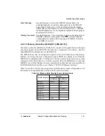
2.2.1.15 ID Select (IDSEL)—Input
Following is the state meaning for IDSEL. See Section 7.3.3.3, “Configuration Space
Addressing,” for more information about the role of the IDSEL signal in PCI configuration
transactions.
State Meaning
Asserted—When the C/BE[3:0] encoding is set to configuration
read/write, IDSEL indicates that the PCI configuration registers on
the MPC8240 are being accessed.
Negated—Indicates that there is no configuration access for this
device in progress.
Note that the MPC8240 must not issue PCI configuration transactions to itself (that is, for
PCI configuration transactions initiated by the MPC8240, its IDSEL signal must not be
asserted). The MPC8240 must use the method described in Section 4.1, “Configuration
Register Access,” to access its own configuration registers. If the MPC8240 is in host mode
and other PCI agents do not need to access the MPC8240’s configuration space, then it is
recommended that this signal be pulled down.
2.2.2 Memory Interface Signals
The memory interface supports either standard DRAMs, extended data out DRAMs (EDO
DRAMs), or synchronous DRAMs (SDRAMs) and either standard ROM or Flash devices.
Some of the memory interface signals perform different functions (and are described by an
alternate name) depending on the RAM and ROM configurations. This section provides a
brief description of the memory interface signals on the MPC8240, listed individually by
both their primary and alternate names, describing the relevant function in each section. For
more information on the operation of the memory interface, see Chapter 6, “MPC8240
Memory Interface.”
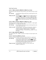
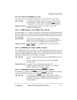
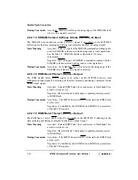
2.2.2.1 Row Address Strobe (RAS[0:7])—Output
The eight row address strobe (RAS[0:7]) signals are outputs on the MPC8240. Following
are the state meaning and timing comments for the RASn output signals.
State Meaning
Asserted—Indicates that the memory row address is valid and selects
one of the rows in the selected bank for DRAM memory.
Negated—Indicates DRAM precharge period.
Timing Comments
Assertion—The MPC8240 asserts the RASn signal to begin a
memory cycle. All other memory interface signal timings are
referenced to RASn.
Summary of Contents for MPC8240
Page 1: ...MPC8240UM D Rev 1 1 2001 MPC8240 Integrated Processor User s Manual ...
Page 38: ...xviii MPC8240 Integrated Processor User s Manual TABLES Table Number Title Page Number ...
Page 48: ...xlviii MPC8240 Integrated Processor User s Manual Acronyms and Abbreviations ...
Page 312: ...6 94 MPC8240 Integrated Processor User s Manual ROM Flash Interface Operation ...
Page 348: ...7 36 MPC8240 Integrated Processor User s Manual PCI Host and Agent Modes ...
Page 372: ...8 24 MPC8240 Integrated Processor User s Manual DMA Register Descriptions ...
Page 394: ...9 22 MPC8240 Integrated Processor User s Manual I2O Interface ...
Page 412: ...10 18 MPC8240 Integrated Processor User s Manual Programming Guidelines ...
Page 454: ...12 14 MPC8240 Integrated Processor User s Manual Internal Arbitration ...
Page 466: ...13 12 MPC8240 Integrated Processor User s Manual Exception Latencies ...
Page 516: ...16 14 Watchpoint Trigger Applications ...
Page 538: ...B 16 MPC8240 Integrated Processor User s Manual Setting the Endian Mode of Operation ...
Page 546: ...C 8 MPC8240 Integrated Processor User s Manual ...
Page 640: ...INDEX Index 16 MPC8240 Integrated Processor User s Manual ...


