background image

Chapter  1.  Overview  

1-7

Processor Core Overview

.

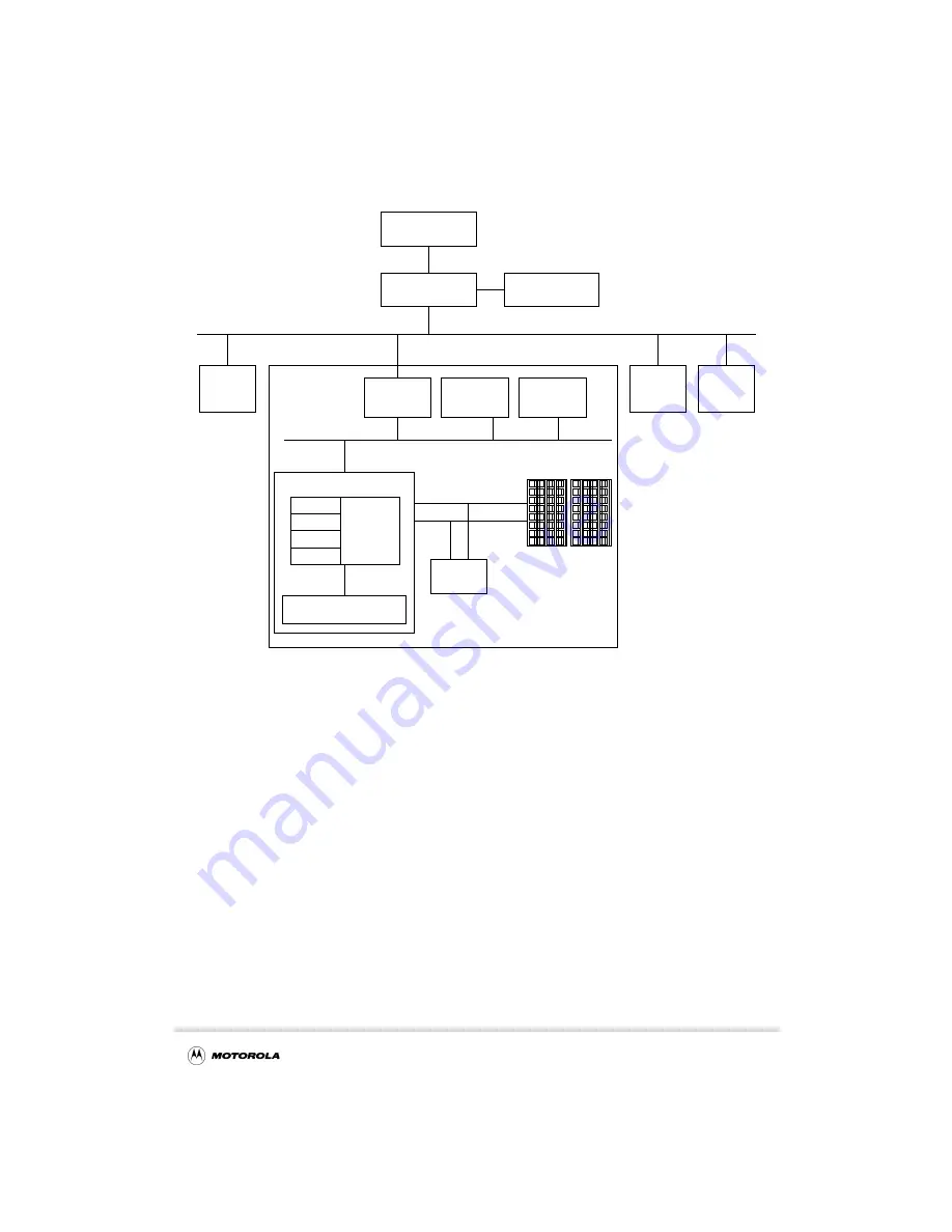
Figure 1-4. Embedded System Using an MPC8240 as a Distributed Processor

1.2  Processor Core Overview

The MPC8240 contains an embedded version of the PowerPC 603e™ processor. For
detailed information regarding the processor refer to the following:

MPC603e & EC603e User’s Manual (Those chapters that describe the 
programming model, cache model, memory management model, exception model, 
and instruction timing) 

PowerPC Microprocessor Family: The Programming Environments for 32-Bit 
Microprocessors

This section is an overview of the processor core, provides a block diagram showing the
major functional units, and describes briefly how those units interact. For more
information, refer to Chapter 2, “PowerPC Processor Core.” 

The processor core is a low-power implementation of the PowerPC microprocessor family
of reduced instruction set computing (RISC) microprocessors. The processor core
implements the 32-bit portion of the PowerPC architecture, which provides 32-bit effective
addresses, integer data types of 8, 16, and 32 bits, and floating-point data types of 32 and
64 bits. 

Host Bridge

Host Processor

Host Memory

Local Memory: 
DRAM, EDO, 
SDRAM

CTRL

Data

Processor Core

MPC8240

PCI Bus

Peripheral

Peripheral

System 

Peripheral 2

PCI-to-PCI

Bridge

Local PCI bus

I/O 

I/O 

Device

Device

1

3

I/O 

Controller

Peripheral 

I

2

C

EPIC

DMA

MU(I

2

O)

Logic

ROM /
Port X

Summary of Contents for MPC8240

Page 1: ...MPC8240UM D Rev 1 1 2001 MPC8240 Integrated Processor User s Manual ...

Page 2: ...orola products are not designed intended or authorized for use as components in systems intended for surgical implant into the body or other applications intended to support or sustain life or for any other application in which the failure of the Motorola product could create a situation where personal injury or death may occur Should Buyer purchase or use Motorola products for any such unintended...

Page 3: ...DMA Controller Message Unit I2O I2C Interface Embedded Programmable Interrupt Controller EPIC Central Control Unit Error Handling Power Management Debug Features Address Map A Bit and Byte Ordering Glossary of Terms and Abbreviations Index B Programmable I O and Watchpoint PowerPC Instruction Set 16 C GLO IND A 15 D E P Processor Core Register Summary Initialization Example 15 ...

Page 4: ...Controller EPIC Central Control Unit Error Handling Power Management Debug Features Address Map A Bit and Byte Ordering Glossary of Terms and Abbreviations Index Programmable I O and Watchpoint Initialization Example 15 1 2 3 4 5 6 7 8 9 10 11 12 13 14 B 16 C GLO IND A D E PowerPC Processor Core MPC8240 Memory Interface 15 PowerPC Instruction Set Processor Core Register Summary 15 ...

Page 5: ...nslation 1 14 1 4 4 3 Byte Ordering 1 15 1 4 4 4 PCI Agent Capability 1 15 1 4 5 DMA Controller 1 15 1 4 6 Message Unit MU 1 15 1 4 6 1 Doorbell Registers 1 15 1 4 6 2 Inbound and Outbound Message Registers 1 16 1 4 6 3 Intelligent Input Output Controller I2O 1 16 1 4 7 Inter Integrated Circuit I2C Controller 1 16 1 4 8 Embedded Programmable Interrupt Controller EPIC 1 16 1 4 9 Integrated PCI Bus ...

Page 6: ...3 PCI Address Data Bus AD 31 0 2 9 2 2 1 3 1 Address Data AD 31 0 Output 2 9 2 2 1 3 2 Address Data AD 31 0 Input 2 9 2 2 1 4 Parity PAR 2 10 2 2 1 4 1 Parity PAR Output 2 10 2 2 1 4 2 Parity PAR Input 2 10 2 2 1 5 Command Byte Enable C BE 3 0 2 10 2 2 1 5 1 Command Byte Enable C BE 3 0 Output 2 10 2 2 1 5 2 Command Byte Enable C BE 3 0 Input 2 11 2 2 1 6 Device Select DEVSEL 2 11 2 2 1 6 1 Device...

Page 7: ... 2 2 2 9 2 Memory Data Bus MDH 0 31 MDL 0 31 Input 2 20 2 2 2 10 Data Parity ECC PAR 0 7 2 20 2 2 2 10 1 Data Parity PAR 0 7 Output 2 20 2 2 2 10 2 Data Parity PAR 0 7 Input 2 21 2 2 2 11 ROM Address 19 12 AR 19 12 Output 2 21 2 2 2 12 SDRAM Clock Enable CKE Output 2 21 2 2 2 13 SDRAM Row Address Strobe SDRAS Output 2 21 2 2 2 14 SDRAM Column Address Strobe SDCAS Output 2 22 2 2 2 15 ROM Bank 0 Se...

Page 8: ... 2 Output 2 30 2 2 5 10 2 PCI Address Attributes PMAA 0 2 Output 2 30 2 2 5 10 3 Debug Address DA 0 15 Output 2 30 2 2 5 10 4 Memory Interface Valid MIV Output 2 31 2 2 6 Test and Configuration Signals 2 31 2 2 6 1 PLL Configuration PLL_CFG 0 4 Input 2 31 2 2 6 2 JTAG Test Clock TCK Input 2 31 2 2 6 3 JTAG Test Data Input TDI Input 2 32 2 2 6 4 JTAG Test Data Output TDO Output 2 32 2 2 6 5 JTAG Te...

Page 9: ...er Access 4 1 4 1 1 Configuration Register Access in Little Endian Mode 4 2 4 1 2 Configuration Register Access in Big Endian Mode 4 3 4 1 3 Configuration Register Summary 4 5 4 1 3 1 Processor Accessible Configuration Registers 4 5 4 1 3 2 PCI Accessible Configuration Registers 4 8 4 2 PCI Interface Configuration Registers 4 10 4 2 1 PCI Command Register Offset 0x04 4 11 4 2 2 PCI Status Register...

Page 10: ...patch Unit 5 6 5 2 3 Branch Processing Unit BPU 5 6 5 2 4 Independent Execution Units 5 6 5 2 4 1 Integer Unit IU 5 7 5 2 4 2 Floating Point Unit FPU 5 7 5 2 4 3 Load Store Unit LSU 5 7 5 2 4 4 System Register Unit SRU 5 8 5 2 5 Completion Unit 5 8 5 2 6 Memory Subsystem Support 5 8 5 2 6 1 Memory Management Units MMUs 5 8 5 2 6 2 Cache Units 5 9 5 2 6 3 Peripheral Logic Bus Interface 5 9 5 2 6 3 ...

Page 11: ...tion Specific Exception Model 5 27 5 5 3 Exception Priorities 5 30 5 6 Memory Management 5 30 5 6 1 PowerPC MMU Model 5 30 5 6 2 MPC8240 Implementation Specific MMU Features 5 31 5 7 Instruction Timing 5 32 5 8 Differences between the MPC8240 Core and the PowerPC 603e Microprocessor 5 34 Chapter 6 MPC8240 Memory Interface 6 1 Memory Interface Signal Summary 6 3 6 2 SDRAM Interface Operation 6 6 6 ...

Page 12: ...EDO DRAM Interface Timing 6 56 6 3 6 DMA Burst Wrap 6 61 6 3 7 FPM or EDO DRAM Page Mode Retention 6 61 6 3 8 FPM or EDO DRAM Parity and RMW Parity 6 61 6 3 8 1 RMW Parity Latency Considerations 6 62 6 3 9 FPM or EDO ECC 6 62 6 3 9 1 FPM or EDO DRAM Interface Timing with ECC 6 64 6 3 10 FPM or EDO DRAM Refresh 6 66 6 3 10 1 FPM or EDO Refresh Timing 6 66 6 3 11 FPM or EDO DRAM Power Saving Modes 6...

Page 13: ... 13 7 3 6 Bus Driving and Turnaround 7 14 7 4 PCI Bus Transactions 7 14 7 4 1 PCI Read Transactions 7 14 7 4 2 PCI Write Transactions 7 16 7 4 3 Transaction Termination 7 17 7 4 3 1 Master Initiated Termination 7 17 7 4 3 2 Target Initiated Termination 7 18 7 4 4 Fast Back to Back Transactions 7 21 7 4 5 Configuration Cycles 7 21 7 4 5 1 The PCI Configuration Space Header 7 21 7 4 5 2 Accessing th...

Page 14: ... 6 8 3 3 DMA Operation Flow 8 7 8 3 4 DMA Coherency 8 8 8 3 5 DMA Performance 8 8 8 4 DMA Transfer Types 8 9 8 4 1 PCI to PCI 8 9 8 4 2 PCI to Local Memory 8 9 8 4 3 Local Memory to PCI 8 9 8 4 4 Local Memory to Local Memory 8 9 8 5 Address Map Interactions 8 10 8 5 1 Attempted Writes to Local ROM Port X Space 8 10 8 5 2 Host Mode Interactions 8 10 8 5 2 1 PCI Master Abort when PCI Bus Specified f...

Page 15: ... Interface 9 5 9 3 1 PCI Configuration Identification 9 5 9 3 2 I2O Register Summary 9 5 9 3 3 FIFO Descriptions 9 6 9 3 3 1 Inbound FIFOs 9 7 9 3 3 1 1 Inbound Free_List FIFO 9 8 9 3 3 1 2 Inbound Post_List FIFO 9 8 9 3 3 2 Outbound FIFOs 9 8 9 3 3 2 1 Outbound Free_List FIFO 9 8 9 3 3 2 2 Outbound Post_List FIFO 9 9 9 3 4 I2O Register Descriptions 9 9 9 3 4 1 PCI Accessible I2O Registers 9 9 9 3...

Page 16: ...Address Transmission 10 4 10 2 3 Data Transfer 10 5 10 2 4 Repeated START Condition 10 5 10 2 5 STOP Condition 10 5 10 2 6 Arbitration Procedure 10 5 10 2 7 Clock Synchronization 10 6 10 2 8 Handshaking 10 7 10 2 9 Clock Stretching 10 7 10 3 I2 C Register Descriptions 10 7 10 3 1 I2 C Address Register I2CADR 10 7 10 3 2 I2 C Frequency Divider Register I2CFDR 10 8 10 3 3 I2C Control Register I2CCR ...

Page 17: ...1 6 1 Sampling of Serial Interrupts 11 11 11 6 2 Serial Interrupt Timing Protocol 11 12 11 6 3 Edge Level Sensitivity of Serial Interrupts 11 12 11 7 EPIC Timers 11 13 11 8 Programming Guidelines 11 13 11 9 Register Definitions 11 16 11 9 1 Feature Reporting Register FRR 11 16 11 9 2 Global Configuration Register GCR 11 16 11 9 3 EPIC Interrupt Configuration Register EICR 11 17 11 9 4 EPIC Vendor ...

Page 18: ...Memory Read Buffers PCMRBs 12 7 12 1 3 1 2 Speculative PCI Reads from Local Memory 12 8 12 1 3 2 PCI to Local Memory Write Buffers PCMWBs 12 8 12 2 Internal Arbitration 12 9 12 2 1 Arbitration Between PCI and DMA Accesses to Local Memory 12 9 12 2 1 1 DMA Transaction Boundaries for Memory Memory Transfers 12 10 12 2 1 2 DMA Transaction Boundaries for Memory to PCI Transfers 12 10 12 2 1 3 DMA Tran...

Page 19: ... 4 Exception Latencies 13 11 Chapter 14 Power Management 14 1 Overview 14 1 14 2 Processor Core Power Management 14 1 14 2 1 Dynamic Power Management 14 2 14 2 2 Programmable Power Modes on Processor Core 14 2 14 2 3 Processor Power Management Modes Details 14 4 14 2 3 1 Full Power Mode with DPM Disabled 14 4 14 2 3 2 Full Power Mode with DPM Enabled 14 4 14 2 3 3 Processor Doze Mode 14 4 14 2 3 4...

Page 20: ...Address Signal Definitions 15 6 15 3 3 Physical Address Mappings 15 6 15 3 4 RAS Encoding 15 7 15 3 5 Debug Address Timing 15 8 15 4 Memory Interface Valid MIV 15 8 15 4 1 MIV Signal Timing 15 9 15 5 Memory Data Path Error Injection Capture 15 17 15 5 1 Memory Data Path Error Injection Mask Registers 15 17 15 5 1 1 DH Error Injection Mask Register 15 17 15 5 1 2 DL Error Injection Mask Register 15...

Page 21: ...13 Appendix A Address Map A A 1 Address Space for Map A A 1 A 2 Configuration Accesses Using Direct Method A 5 Appendix B Bit and Byte Ordering B 1 Byte Ordering Overview B 1 B 2 Byte Ordering Mechanisms B 1 B 3 Big Endian Mode B 2 B 4 Little Endian Mode B 5 B 4 1 I O Addressing in Little Endian Mode B 15 B 5 Setting the Endian Mode of Operation B 15 Appendix C Initialization Example Appendix D Po...

Page 22: ...t E 11 E 1 3 1 Machine State Register MSR E 13 E 1 3 2 Processor Version Register PVR E 15 E 1 3 3 BAT Registers E 15 E 1 3 4 SDR1 E 17 E 1 3 5 Segment Registers E 18 E 1 3 6 SPRG0 SPRG3 E 18 E 1 3 7 DSISR E 19 E 1 3 8 Machine Status Save Restore Register 0 SRR0 E 19 E 1 3 9 Time Base Facility TB OEA Writing to the Time Base E 19 E 1 3 10 Decrementer Register DEC E 19 E 1 3 11 External Access Regi...

Page 23: ...essor Options in Host Mode 3 9 3 5 Address Map B PCI Options in Host Mode 3 10 3 6 Inbound PCI Address Translation 3 12 3 7 Outbound PCI Address Translation 3 13 3 8 Local Memory Base Address Register LMBAR 0x10 3 15 3 9 Inbound Translation Window Register ITWR 3 15 3 10 Outbound Memory Base Address Register OMBAR 0x0_2300 3 16 3 11 Outbound Translation Window Register OTWR 0x0_2308 3 17 3 12 Embe...

Page 24: ...CCR2 0xF4 4 45 4 31 Memory Control Configuration Register 3 MCCR3 0xF8 4 48 4 32 Memory Control Configuration Register 4 MCCR4 0xFC 4 51 5 1 MPC8240 Integrated Processor Core Block Diagram 5 2 5 2 MPC8240 Programming Model Registers 5 12 5 3 Hardware Implementation Register 0 HID0 5 13 5 4 Hardware Implementation Register 1 HID1 5 16 5 5 Hardware Implementation Dependent Register 2 HID2 5 17 5 6 D...

Page 25: ...59 6 38 DRAM Single Beat Write Timing No ECC 6 59 6 39 DRAM Four Beat Burst Write Timing No ECC 64 Bit Mode 6 60 6 40 DRAM Eight beat Burst Write Timing No ECC 32 Bit Mode 6 60 6 41 FPM DRAM Burst Read with ECC 6 65 6 42 EDO DRAM Burst Read Timing with ECC 6 65 6 43 DRAM Single Beat Write Timing with RMW or ECC Enabled 6 66 6 44 DRAM Bank Staggered CBR Refresh Timing Configuration 6 67 6 45 DRAM S...

Page 26: ...on 7 16 7 5 PCI Single Beat Write Transaction 7 16 7 6 PCI Burst Write Transaction 7 17 7 7 PCI Target Initiated Terminations 7 20 7 8 Standard PCI Configuration Header 7 22 7 9 CONFIG_ADDR Register Format 7 24 7 10 Type 0 Configuration Translation 7 25 7 11 PCI Parity Operation 7 31 8 1 DMA Controller Block Diagram 8 2 8 2 DMA Controller General Flow 8 7 8 3 Chaining of DMA Descriptors in Memory ...

Page 27: ...on Block Diagram Non programmable Registers 11 9 11 3 Serial Interrupt Interface Protocol 11 12 11 4 Feature Reporting Register FRR 11 16 11 5 Global Configuration Register GCR 11 16 11 6 EPIC Interrupt Configuration Register EICR 11 17 11 7 EPIC Vendor Identification Register EVI 11 18 11 8 Processor Initialization Register PI 11 19 11 9 Spurious Vector Register SVR 11 19 11 10 Timer Frequency Re...

Page 28: ...rite Operation 15 14 15 14 Example ROM Debug Address MIV and MAA Timings For Burst Read 15 15 15 15 Example Flash Debug Address MIV and MAA Timings For Single Byte Read 15 16 15 16 Example Flash Debug Address MIV and MAA Timings for Write Operation 15 16 15 17 Functional Diagram of Memory Data Path Error Injection 15 17 15 18 DH Error Injection Mask MDP_ERR_INJ_MASK_DH Offsets 0xF_F000 0xF00 15 17...

Page 29: ...dian PCI Memory Space B 5 B 4 Munged Memory Image in Local Memory B 7 B 5 Little Endian Memory Image in Little Endian PCI Memory Space B 8 B 6 One Byte Transfer to PCI Memory Space Little Endian Mode B 9 B 7 Two Byte Transfer to PCI Memory Space Little Endian Mode B 10 B 8 Four Byte Transfer to PCI Memory Space Little Endian Mode B 11 B 9 One Byte Transfer to PCI I O Space Little Endian Mode B 12 ...

Page 30: ...SRR1 E 19 E 20 Decrementer Register DEC E 20 E 21 External Access Register EAR E 20 E 22 DMISS and IMISS Registers E 21 E 23 DCMP and ICMP Registers E 21 E 24 HASH1 and HASH2 Registers E 22 E 25 Required Physical Address Register RPA E 22 E 26 Instruction Address Breakpoint Register IABR E 23 E 27 Hardware Implementation Register 0 HID0 E 24 E 28 Hardware Implementation Register 1 HID1 E 27 E 29 H...

Page 31: ...00 3 17 3 11 Bit Settings for OTWR 0x0_2308 3 17 3 12 Embedded Utilities Local Memory Register Summary 3 19 3 13 Embedded Utilities Peripheral Control and Status Register Summary 3 20 4 1 Internal Register Access Port Locations 4 1 4 2 MPC8240 Configuration Registers Accessible from the Processor Core 4 5 4 3 MPC8240 Configuration Registers Accessible from the PCI Bus 4 9 4 4 PCI Configuration Spa...

Page 32: ...gs for Error Enabling Register 2 ErrEnR2 0xC4 4 38 4 34 Bit Settings for Error Detection Register 2 ErrDR2 0xC5 4 39 4 35 Bit Settings for PCI Bus Error Status Register 0xC7 4 40 4 36 Bit Settings for Processor PCI Error Address Register 0xC8 4 40 4 37 Bit Settings for the AMBOR 0xE0 4 41 4 38 Bit Settings for MCCR1 0xF0 4 43 4 39 Bit Settings for MCCR2 0xF4 4 46 4 40 Bit Settings for MCCR3 0xF8 4...

Page 33: ...ations of ROM Flash Controller 6 76 7 1 PCI Arbiter Control Register Parking Mode Bits 7 8 7 2 PCI Bus Commands 7 10 7 3 Supported Combinations of AD 1 0 7 12 7 4 PCI Configuration Space Header Summary 7 22 7 5 CONFIG_ADDR Register Fields 7 24 7 6 Type 0 Configuration Device Number to IDSEL Translation 7 26 7 7 Special Cycle Message Encodings 7 28 7 8 Initialization Options for PCI Controller 7 33...

Page 34: ...t 0x0_3000 10 8 10 4 I2CFDR Field Descriptions Offset 0x0_3004 10 8 10 5 Serial Bit Clock Frequency Divider Selections 10 9 10 6 I2CCR Field Descriptions Offset 0x0_3008 10 10 10 7 I2CSR Field Descriptions Offset 0x0_300C 10 12 10 8 I2CDR Field Descriptions Offset 0x0_3010 10 13 11 1 EPIC Interface Signal Description 11 2 11 2 EPIC Register Address Map Global and Timer Registers 11 4 11 3 EPIC Reg...

Page 35: ... Mask Bit Field Definitions 15 18 15 9 DL Error Injection Mask Bit Field Definitions 15 18 15 10 Parity Error Injection Mask Bit Field Definitions 15 19 15 11 DH Error Capture Monitor Bit Field Definitions 15 19 15 12 DL Error Capture Monitor Bit Field Definitions 15 20 15 13 Parity Error Capture Monitor Bit Field Definitions 15 20 16 1 Watchpoint Signal Summary 16 2 16 2 Watchpoint Register Offse...

Page 36: ...le Instructions D 22 D 17 Integer Load and Store String Instructions D 22 D 18 Memory Synchronization Instructions D 22 D 19 Floating Point Load Instructions7 D 23 D 20 Floating Point Store Instructions7 D 23 D 21 Floating Point Move Instructions7 D 23 D 22 Branch Instructions D 24 D 23 Condition Register Logical Instructions D 24 D 24 System Linkage Instructions D 24 D 25 Trap Instructions D 24 D...

Page 37: ...oint Exception Mode Bits E 15 E 10 BAT Registers Field and Bit Descriptions E 16 E 11 BAT Area Lengths E 17 E 12 SDR1 Bit Settings E 17 E 13 Segment Register Bit Settings T 0 E 18 E 14 Conventional Uses of SPRG0 SPRG3 E 18 E 15 External Access Register EAR Bit Settings E 20 E 16 DCMP and ICMP Bit Settings E 21 E 17 HASH1 and HASH2 Bit Settings E 22 E 18 RPA Bit Settings E 23 E 19 Instruction Addre...

Page 38: ...xviii MPC8240 Integrated Processor User s Manual TABLES Table Number Title Page Number ...

Page 39: ...e is designed to support a broad range of processors The Programming Environments Manual provides a general description of features that are common to PowerPC processors and indicates those features that are optional or may be implemented differently in the design of each processor The information is subject to change without notice as described in the disclaimers on the title page of this book As...

Page 40: ...cessor and PCI interactions to main memory Chapter 7 PCI Bus Interface provides a rudimentary description of PCI bus operations The specific emphasis is directed at how the MPC8240 implements the PCI bus Chapter 8 DMA Controller describes how the DMA controller operates on the MPC8240 Chapter 9 Message Unit with I2O describes a mechanism to facilitate communications between host and peripheral pro...

Page 41: ...ing environments of the PowerPC architecture Suggested Reading This section lists additional reading that provides background for the information in this manual as well as general information about the PowerPC architecture General Information The following documentation provides useful information about the PowerPC architecture and computer architecture in general The following books are available...

Page 42: ...werPC architecture that are common to PowerPC processors The 32 bit architecture model is described in PowerPC Microprocessor Family The Programming Environments for 32 Bit Microprocessors Rev 1 MPCFPE32B AD Motorola order Implementation Variances Relative to Rev 1 of The Programming Environments Manual is available via the world wide web at http www motorola com PowerPC Addenda errata to user s m...

Page 43: ...PC implementations is being released as new processors become available For a current list of PowerPC documentation refer to the world wide web at http www mot com SPS PowerPC Conventions This document uses the following notational conventions mnemonics Instruction mnemonics are shown in lowercase bold italics Italics indicate variable command parameters for example bcctrx Book titles in text are ...

Page 44: ...ated Terms Term Meaning ALU Arithmetic logic unit BAT Block address translation BGA Ball grid array package BIST Built in self test BIU Bus interface unit BPU Branch processing unit CAR Cache address register CAS Column address strobe CBR CAS before RAS CIA Current instruction address CMOS Complementary metal oxide semiconductor CR Condition register CRTRY Cache retry queue CTR Count register DAR ...

Page 45: ...B compare IEEE Institute for Electrical and Electronics Engineers Int Ack Interrupt acknowledge IMISS Instruction TLB miss address IQ Instruction queue ISA Industry standard architecture ITLB Instruction translation lookaside buffer IU Integer unit JTAG Joint test action group interface L2 Secondary cache LIFO Last in first out LR Link register LRU Least recently used LSB Least significant byte ls...

Page 46: ...table entry PTEG Page table entry group PVR Processor version register RAS Row address strobe RAW Read after write RISC Reduced instruction set computing ROM Read only memory RPA Required physical address RTL Register transfer language RWITM Read with intent to modify SDR1 Register that specifies the page table base address for virtual to physical address translation SDRAM Synchronous dynamic rand...

Page 47: ...ction set architecture UUT Unit under test VCO Voltage controlled oscillator VEA Virtual environment architecture WAR Write after read WAW Write after write WIMG Write through caching inhibited memory coherency enforced guarded bits XER Register used for indicating conditions such as carries and overflows for integer operations Table i Acronyms and Abbreviated Terms Continued Term Meaning ...

Page 48: ...xlviii MPC8240 Integrated Processor User s Manual Acronyms and Abbreviations ...

Page 49: ...unications and other embedded markets It can be used for control processing in applications such as network routers and switches mass storage subsystems network appliances and print and imaging systems For errata or revisions to this document refer to the web site at http www motorola com semiconductors 1 1 MPC8240 Integrated Processor Overview The MPC8240 integrated processor is comprised of a pe...

Page 50: ...oller DMA Controller Interrupt Controller EPIC Timers PCI Bus Interface Unit Memory Controller Data Path ECC Controller Central Control Unit 32 Bit OSC In Five Request Grant Pairs I2C 5 IRQs Processor Core Block Peripheral Logic Block Processor PLL 64 bit Two instruction Fetch 64 bit Two instruction Dispatch Peripheral Logic PLL SDRAM Clocks PCI Clock In PCI Bus Clocks Data 64 bit Address Data Bus...

Page 51: ...l logic to be optimized for performance PCI accesses to the MPC8240 s memory space are passed to the processor bus for snooping when snoop mode is enabled The processor core and peripheral logic are general purpose in order to serve a variety of embedded applications The MPC8240 can be used as either a PCI host or PCI agent controller 1 1 1 MPC8240 Integrated Processor Features This section summar...

Page 52: ...atic linking of DMA transfers Supports scatter gathering read or write discontinuous memory Interrupt on completed segment chain and error Local to local memory PCI to PCI memory PCI to local memory PCI memory to local memory Message unit Two doorbell registers Two inbound and two outbound messaging registers I2O message controller I2C controller with full master slave support except broadcast all...

Page 53: ...way basis 1 1 2 MPC8240 Integrated Processor Applications The MPC8240 can be used for control processing in applications such as routers switches multi channel modems network storage image display systems enterprise I O processor Internet access device IAD disk controller for RAID systems and copier printer board control Figure 1 2 shows the MPC8240 in the role of host processor Figure 1 2 System ...

Page 54: ... variety The MPC8240 would not be part of the system configuration map This configuration is useful in applications such as RAID controllers where the I O devices shown are SCSI controllers or multi port network controllers where the devices shown are Ethernet controllers PCI Bus Peripheral Peripheral PCI to PCI Bridge PCI Bus System Peripheral 2 Local Memory DRAM EDO SDRAM CTRL Data Processor Cor...

Page 55: ...ides a block diagram showing the major functional units and describes briefly how those units interact For more information refer to Chapter 2 PowerPC Processor Core The processor core is a low power implementation of the PowerPC microprocessor family of reduced instruction set computing RISC microprocessors The processor core implements the 32 bit portion of the PowerPC architecture which provide...

Page 56: ... virtual memory address translation and variable sized block translation The TLBs and caches use a least recently used LRU replacement algorithm The processor also supports block address translation through the use of two independent instruction and data block address translation IBAT and DBAT arrays of four entries each Effective addresses are compared simultaneously with all four entries in the ...

Page 57: ...FPSCR SYSTEM REGISTER UNIT PERIPHERAL LOGIC BUS INTERFACE D MMU SRs DTLB DBAT Array Touch Load Buffer Copyback Buffer 64 Bit 32 Bit Dispatch Unit 64 Bit 64 Bit Power Dissipation Control COMPLETION UNIT Time Base Counter Decrementer Clock Multiplier JTAG COP Interface XER I MMU SRs ITLB IBAT Array 16Kbyte I Cache Tags 64 Bit 64 Bit 64 Bit 64 Bit 64 Bit GPR File LOAD STORE UNIT 64 Bit GPRename Regis...

Page 58: ...the peripheral logic bus to allow the processor to snoop these accesses when snooping not explicitly disabled As part of the peripheral logic bus interface the processor core s data bus is configured at power up to either a 32 or 64 bit width When the processor is configured with a 32 bit data bus memory accesses on the peripheral logic bus interface allow transfer sizes of 8 16 24 or 32 bits in o...

Page 59: ...cally implemented Figure 1 6 MPC8240 Peripheral Logic Block Diagram 1 4 1 Peripheral Logic Features Major features of the peripheral logic are as follows Peripheral logic bus Supports various operating frequencies and bus divider ratios 32 bit address bus 64 bit data bus Supports full memory coherency Peripheral Logic Address Translator DLL Fanout Buffers PCI Arbiter Message Unit with I2O I2C Cont...

Page 60: ...ce may be split between the PCI bus and the memory bus 8 Mbytes each Supports 8 bit asynchronous ROM or 32 or 64 bit burst mode ROM Supports writing to flash ROM Configurable data path Programmable interface timing PCI interface Compatible with PCI Local Bus Specification Revision 2 1 Supports PCI locked accesses to memory using the LOCK signal and protocol Supports accesses to all PCI address spa...

Page 61: ...he MPC8240 Some devices may require a small amount of external logic to generate properly address strobes chip selects and other signals The MPC8240 is designed to control a 32 or 64 bit data path to main memory DRAM or SDRAM For a 32 bit data path the MPC8240 can be configured to check and generate byte parity using four parity bits For a 64 bit data path the MPC8240 can be configured to support ...

Page 62: ...evice can be programmed within a pool of a high or low priority arbitration One member of the low priority pool is promoted to the high priority pool As soon as it is granted the bus it returns to the low priority pool The unit can be disabled to allow a remote arbitration unit to be used 1 4 4 2 Address Maps and Translation The MPC8240 s processor bus supports memory mapped accesses The address s...

Page 63: ...The DMA controller allows chaining through local memory mapped chain descriptors Transfers can be scatter gathered and misaligned Interrupts are provided on completed segment chain and error conditions 1 4 6 Message Unit MU Many embedded applications require handshake algorithms to pass control status and data information from one owner to another This is made easier with doorbell and message regi...

Page 64: ... of the MU enhances communication between hosts and IOPs within a system There are two paths for messages an inbound queue is used to transfer messages from a remote host or IOP to the processor core and an outbound queue is used to transfer messages from the processor core to the remote host Each queue is implemented as a pair of FIFOs The inbound and outbound message queues each consists of a fr...

Page 65: ...ock loads five clock fanout buffers are provided on chip For systems requiring more clock fan out or where the MPC8240 is an agent device external clock buffers may be used The MPC8240 provides an on chip delay locked loop DLL that supplies the external memory bus clock signals to SDRAM banks The memory bus clock signals are of the same frequency and synchronous with the internal peripheral bus cl...

Page 66: ...available in the MPC603e device 1 5 2 Programmable Peripheral Logic Power Management Modes The following subsections describe the power management modes of the peripheral logic Table 1 2 summarizes the programmable power saving modes for the peripheral logic block Table 1 1 Programmable Processor Power Modes PM Mode Functioning Units Activation Method Full Power Wake Up Method Full power All units...

Page 67: ...request and NMI monitoring EPIC unit I2C unit PLL Controlled by software write to PMCR1 PCI access to memory Processor bus request Assertion of NMI1 Interrupt to EPIC Hard Reset 1 Programmable option based on value of PICR1 MCP_EN 1 Nap PCI address decoding and bus arbiter System RAM refreshing Processor bus request and NMI monitoring EPIC unit I2C unit PLL Controlled by software write to PMCR1 an...

Page 68: ...ress pins are sampled at the same time as the ROM address and can be used to recreate the 24 bit physical address in conjunction with ROM address The granularity of the reconstructed physical address is limited by the bus width of the interface double words for 64 bit interfaces words for 32 bit interfaces and bytes for 8 bit interfaces 1 7 3 Memory Interface Valid MIV The memory interface valid s...

Page 69: ...depicted as lower case and in italics For example sys_logic_clk is an internal signal These are referenced only as necessary for understanding of the external functionality of the device The chapter is organized into the following sections Overview of signals and complete cross reference for signals that serve multiple functions Includes listing of output signal states at reset Signal description ...

Page 70: ...ug signals Test configuration signals Clock signals Figure 2 1 illustrates the external signals of the MPC8240 showing how the signals are grouped Refer to the MPC8240 Hardware Specification for a pinout diagram showing actual pin numbers and a listing of all the electrical and mechanical specifications ...

Page 71: ...C_IN HRST_CPU 5 4 1 1 1 1 SDRAM_CLK 0 3 1 NMI SRESET 1 CKO DA1 1 PCI_SYNC_OUT PCI_SYNC_IN 1 1 MCP 1 CHKSTOP_IN 1 SMI REQ 3 0 1 GNT 3 0 IRQ0 S_INT 1 1 IDSEL 4 3 1 6 PMAA 0 2 DA 15 11 DA2 1 TCK IRQ3 S_FRAME IRQ4 L_INT 1 1 MAA 0 2 3 Test TDO TMS TRST 1 1 1 1 TDI Clock Interface Interface EPIC Control 1 SCL SDA 1 I2C Control TBEN 1 1 HRST_CTRL 1 IRQ1 S_CLK SDMA 11 0 12 MIV SERR 1 SDBA0 1 MDL 0 31 32 M...

Page 72: ...1 5 CHKSTOP_IN Checkstop in System Control 1 I 2 2 5 6 CKE1 SDRAM clock enable Memory 1 O 2 2 2 12 CKO Debug clock Clock DA1 1 O 2 2 7 8 CS 0 7 SDRAM chip select Memory RAS 0 7 8 O 2 2 2 3 DA 15 11 DA2 Debug addr 15 11 2 Debug 6 O 2 2 5 10 3 DA 10 6 Debug addr 10 6 Debug PLL_CFG 0 4 5 O 2 2 5 10 3 DA5 DA4 DA3 DA1 DA0 Debug addr 5 Debug addr 4 Debug addr 3 Debug addr 1 Debug addr 0 Debug GNT4 REQ4 ...

Page 73: ... DA3 5 O 2 2 7 2 PCI_SYNC_OUT PCI clock output Clock 1 O 2 2 7 3 PCI_SYNC_IN PCI clock input Clock 1 I 2 2 7 4 PERR Parity error PCI 1 I O 2 2 1 11 PLL_CFG 0 4 1 PLL configuration Test Configurati on DA 10 6 5 I 2 2 6 1 PMAA 0 2 1 PCI addr attributes Debug 3 O 2 2 5 10 2 QACK1 Quiesce acknowledge Power Management DA0 1 O 2 2 5 8 RAS 0 7 Row address strobe 0 7 Memory CS 0 7 8 O 2 2 2 1 RCS01 ROM ba...

Page 74: ...m error PCI 1 I O 2 2 1 12 S_FRAME Serial interrupt frame EPIC Control IRQ3 1 I O 2 2 3 2 4 S_INT Serial interrupt stream EPIC Control IRQ0 1 I 2 2 3 2 1 SMI System management interrupt System Control 1 I 2 2 5 5 S_RST Serial interrupt reset EPIC Control IRQ2 1 I O 2 2 3 2 3 SRESET Soft reset System Control 1 I 2 2 5 2 STOP Stop PCI 1 I O 2 2 1 13 TBEN Time base enable System Control 1 I 2 2 5 7 T...

Page 75: ... Interface Signals This section provides descriptions of the PCI interface signals on the MPC8240 Note that throughout this manual signals and bits of the PCI interface are referenced in little endian format For more information on the operation of the MPC8240 PCI interface see Chapter 7 PCI Bus Interface Refer to the PCI Local Bus Specification Revision 2 1 for a thorough description of the PCI l...

Page 76: ...this case the REQ0 becomes the PCI bus grant input for the MPC8240 and it is asserted when the external arbiter is granting the use of the PCI bus to the MPC8240 Note that if the REQ0 input signal is asserted prior to the need to run a PCI transaction then the MPC8240 GNT0 signal will not assert the bus is parked when a PCI transaction is to be run The REQ 4 1 input signals are ignored when the in...

Page 77: ...t the bus is parked when a PCI transaction is to be run Following is the state meaning for the GNT 4 0 input signals when the internal arbiter is disabled State Meaning Asserted The MPC8240 asserts the GNT0 signal as the PCI bus request output signal GNT 4 1 signals do not assert in this case Negated The GNT 4 1 signals are driven high negated in this mode GNT0 is negated when the MPC8240 is not r...

Page 78: ...t signal State Meaning Asserted Indicates odd parity driven by another PCI master or the PCI target during read data phases Negated Indicates even parity driven by another PCI master or the PCI target during read data phases 2 2 1 5 Command Byte Enable C BE 3 0 The four command byte enable C BE 3 0 signals are both input and output signals on the MPC8240 2 2 1 5 1 Command Byte Enable C BE 3 0 Outp...

Page 79: ...ect DEVSEL signal is both an input and output on the MPC8240 2 2 1 6 1 Device Select DEVSEL Output Following is the state meaning for DEVSEL as an output State Meaning Asserted Indicates that the MPC8240 has decoded the address of a PCI transaction and it is the target of the current access Negated Indicates that the MPC8240 has decoded the address and is not the target of the current access Table...

Page 80: ...hat the PCI bus is idle 2 2 1 7 2 Frame FRAME Input Following is the state meaning for FRAME as an input signal State Meaning Asserted Indicates that another PCI master is initiating a bus transaction and causes the MPC8240 to decode the address and the command signals to see if it is the target of the transaction Negated Indicates that the transaction is in the final data phase or that the bus is...

Page 81: ...that a master is requesting exclusive access to memory which may require multiple transactions to complete Negated Indicates that a normal operation is occurring on the bus or an access to a locked target is occurring 2 2 1 10 Target Ready TRDY The target ready TRDY signal is both an input and output signal on the MPC8240 2 2 1 10 1 Target Ready TRDY Output Following is the state meaning for TRDY ...

Page 82: ...arity errors The PCI initiator drives PERR on read operations the PCI target drives PERR on write operations 2 2 1 11 1 Parity Error PERR Output Following is the state meaning for PERR as an output signal State Meaning Asserted Indicates that the MPC8240 acting as a PCI agent detected a data parity error Negated Indicates no error 2 2 1 11 2 Parity Error PERR Input Following is the state meaning f...

Page 83: ...the STOP signal 2 2 1 13 1 Stop STOP Output Following is the state meaning for STOP as an output signal State Meaning Asserted Indicates that the MPC8240 acting as a PCI target is requesting that the initiator stop the current transaction Negated Indicates that the current transaction can continue 2 2 1 13 2 Stop STOP Input Following is the state meaning for STOP as an input signal State Meaning A...

Page 84: ...ed that this signal be pulled down 2 2 2 Memory Interface Signals The memory interface supports either standard DRAMs extended data out DRAMs EDO DRAMs or synchronous DRAMs SDRAMs and either standard ROM or Flash devices Some of the memory interface signals perform different functions and are described by an alternate name depending on the RAM and ROM configurations This section provides a brief d...

Page 85: ... 2 2 2 3 SDRAM Command Select CS 0 7 Output The eight SDRAM command select CS 0 7 signals are output on the MPC8240 Following are the state meaning and timing comments for the CSn output signals State Meaning Asserted Selects an SDRAM bank to perform a memory operation Negated Indicates no SDRAM action during the current cycle Timing Comments Assertion The MPC8240 asserts the CSn signal to begin a...

Page 86: ...hase of the transaction See Section 6 2 2 SDRAM Address Multiplexing for a complete description of the mapping of these signals in all cases Timing Comments Assertion For DRAM the row address is considered valid on the assertion of RASn and the column address is valid on the assertion of CASn For SDRAM the row address is valid on the rising edge of SDRAM_CLK 0 3 clock signals when CSn is asserted ...

Page 87: ...s on the MPC8240 The data bus is comprised of two halves data bus high MDH 0 31 and data bus low MDL 0 31 The MPC8240 can also be configured to operate with a 32 bit data bus on the memory interface by driving the reset configuration signal MDL0 low during reset When the MPC8240 is configured with a 32 bit data bus the bus operates in the same way as when configured with a 64 bit data bus with the...

Page 88: ...nal State Meaning Asserted Negated Represents the value of data being driven by the memory subsystem on a read Timing Comments Assertion Negation For a memory read transaction the data bus signals are valid at a time dependent on the memory interface configuration parameters Refer to Chapter 4 Configuration Registers and Chapter 6 MPC8240 Memory Interface for more information 2 2 2 10 Data Parity ...

Page 89: ... Address Multiplexing Timing Comments Assertion Negation The ROM address is valid on assertion of RCS0 or RCS1 2 2 2 12 SDRAM Clock Enable CKE Output The SDRAM clock enable CKE signal is an output on the MPC8240 and is also used as a reset configuration input signal CKE is part of the SDRAM command encoding See Section 6 2 SDRAM Interface Operation for more information Following are the state mean...

Page 90: ...tput The ROM bank0 select RCS0 signal is an output on the MPC8240 and a reset configuration input signal Following are the state meaning and timing comments for the RCS0 output signal State Meaning Asserted Selects ROM bank 0 for a read access or Flash bank 0 for a read or write access Negated Deselects bank 0 indicating no pending memory access to ROM Flash Timing Comments Assertion The MPC8240 a...

Page 91: ... MCCR2 register AS is also a reset configuration input signal State Meaning Asserted Programmable number of clocks ASFALL from the assertion of RCS0 or RCS1 Negated Programmable number of clocks ASRISE from the assertion of AS 2 2 3 EPIC Control Signals There are five EPIC interrupt control signals that have dual functions The signals serve as five distinct incoming interrupt requests IRQ 0 4 when...

Page 92: ...polarity These interrupts are clocked in to the MPC8240 by the S_CLK signal 2 2 3 2 2 Serial Interrupt Clock S_CLK Output This output serves as the serial clock that the external interrupt source must use for driving the 16 interrupts onto the S_INT signal State Meaning Asserted Negated The frequency of this clock signal is programmed in the serial interrupt configuration register 2 2 3 2 3 Serial...

Page 93: ...slave State Meaning Asserted Negated Used to drive the data 2 2 4 1 2 Serial Data SDA Input Following is the state meaning of the SDA input signal when the MPC8240 is receiving data State Meaning Asserted Negated Used to receive data from other devices The bus is assumed to be busy when SDA is detected low 2 2 4 2 Serial Clock SCL This signal is an input when the MPC8240 is programmed as an I2C sl...

Page 94: ...ls 2 2 5 1 2 Hard Reset Peripheral Logic HRST_CTRL Input The following describes the state meaning and timing for the HRST_CTRL input signal State Meaning Asserted Negated See Section 2 1 2 Output Signal States during Reset and Section 2 4 Configuration Signals Sampled at Reset for more information on the interpretation of the other MPC8240 signals during reset Timing Comments Assertion Negation S...

Page 95: ...ted depending upon the software configuration Assertion of mcp causes the processor core to conditionally take a machine check exception or enter the checkstop state based on the setting of the MSR ME bit in the processor core Negated There is no mcp being reported to the processor core Timing Comments Assertion mcp may be asserted to the processor core in any cycle so the same timing applies to M...

Page 96: ... CHKSTOP_IN signal State Meaning Asserted Indicates that the MPC8240 processor core must terminate operation by internally gating off all clocks and releasing all processor related outputs to the high impedance state Negated Indicates that normal operation should proceed Timing Comments Assertion May occur at any time and may be asserted asynchronously to the input clocks Negation Must remain asse...

Page 97: ...alue of the WP_RUN bit in the WP_CONTROL register to toggle turning the watchpoint facility on or off See Chapter 16 Programmable I O and Watchpoint for more information Negated No action taken Timing Comments Assertion Negation The MPC8240 interprets TRIG_IN as asserted on detection of the rising edge of TRIG_IN Only required to be asserted for a single clock cycle 2 2 5 9 2 Watchpoint Trigger Ou...

Page 98: ...sserted Negated These signals are encoded to provide more detailed information about a PCI transaction See Section 15 2 3 PCI Address Attribute Signals for a table showing these encodings Timing Comments Assertion Negation Section 15 2 4 PCI Address Attribute Signal Timing contains timing diagrams showing the relative timing of these signals and the rest of the PCI interface 2 2 5 10 3 Debug Addre...

Page 99: ...e PCI clock the processor core frequency and the sys_logic_clk signal that determines the frequency of the memory interface clock The multiplier factor determined by these signals on reset is stored in HID1 PLLRATIO However system software cannot read the PLLRATIO value and associate it with a unique PLL_CFG 0 4 value See Section 5 3 1 2 2 Hardware Implementation Dependent Register 1 HID1 for more...

Page 100: ...aning for the TMS input signal State Meaning Asserted Negated This signal is decoded by the internal JTAG TAP controller to distinguish the primary operation of the test support circuitry Note that this input contains an internal pull up resistor to ensure that an unterminated input appears as a high signal level to the test logic 2 2 6 6 JTAG Test Reset TRST Input The test reset TRST signal is an...

Page 101: ...nce clock The frequency of the PLL outputs is based on the PLL clock frequency configuration signal settings at reset See the MPC8240 Hardware Specification for a complete listing of supported PLL_CFG 0 4 settings 2 2 7 5 SDRAM Clock Outputs SDRAM_CLK 0 3 Output The MPC8240 provides four low skew copies of the SDRAM clock for use in small memory subsystems This clock is synchronized to the on chip...

Page 102: ...he signal on this output is derived from a variety of internal signals after passing through differing numbers of internal buffers This signal is intended for use during system debug it is not intended as a reference clock signal 2 3 Clocking The following sections describe the clocking on the MPC8240 2 3 1 Clocking Method The MPC8240 allows for multiple clock options to suit the needs of various ...

Page 103: ...d by the PLL_CFG 0 4 signals at reset For a given PCI frequency these signals set the peripheral logic frequency and PLL VCO frequency of operation and determine the available multiplier frequencies for the processor core The multiplier for the processor s PLL is further defined by PLL_CFG 0 4 and represented by the value in HID1 PLLRATIO See Section 5 3 1 2 2 Hardware Implementation Dependent Reg...

Page 104: ... register that controls the initial tap point of the DLL Note that although this bit is cleared after a hard reset it must be explicitly set and then cleared by software during initialization in order to guarantee correct operation of the DLL and the SDRAM_CLK 0 3 signals if they are used Therefore care must be taken when using SDRAM_CLK 0 3 to clock peripheral logic as these clocks are not guaran...

Page 105: ...locking System Solution Examples This section describes two example clocking solutions for different system requirements For systems where the MPC8240 is the host controller with a minimum number of clock loads clock fanout buffers are provided on chip shown in Figure 2 5 For systems requiring more clock fanout or where the MPC8240 is an agent device external clock buffers may be used as shown in ...

Page 106: ...on at the negation of the HRST_CTRL and HRST_CPU signals Note that throughout this manual the reset configuration signals are described as being sampled at the negation of reset However the DLL PLL OSC PLL Processor Core Local Memory 66 100 MHz Core Clk PCI Clocks 20 66 MHz Peripheral Logic Clocks sys_logic_clk MPC8240 DLL PLL OSC PLL Processor Core Local Memory 66 6 75 83 3 100 MHz Core Clk PCI C...

Page 107: ...d by PMCR1 CKO_MODE field MDL 0 FOE 11 Sets the initial ROM bank 0 data path width DBUS_SIZE 0 1 values in MCCR1 DBUS_SIZE 0 1 MDL 0 FOE at reset For ROM FLASH chip select 0 RCS0 MDL 0 0 FOE 0 32 bit data bus MDL 0 x FOE 1 8 bit data bus MDL 0 1 FOE 0 64 bit data bus For ROM FLASH chip select 1 RCS1 and memory data bus MDL 0 0 FOE x 32 bit data bus MDL 0 1 FOE x 64 bit data bus MAA0 1 Initial addr...

Page 108: ...s 25 Ω 1 Medium drive capability on PCI signals 50 Ω QACK 1 Clock flip disable When this signal is low on reset it enables internal clock flipping logic which is necessary when the PLL 0 4 signals select a half clock frequency ratio See Section 2 3 3 Clock Synchronization for more information on the use of clock flipping 0 Clock flip enabled 1 No clock flip RCS0 1 Boot memory location The setting ...

Page 109: ...g as a PCI host or agent For more information on the reset configuration signals see Section 2 4 Configuration Signals Sampled at Reset Address map A conforms to the now obsolete PowerPC reference platform PReP specification It is strongly recommended that new designs use map B because map A may not be supported in future devices For this reason address map A is not described in this chapter inste...

Page 110: ..._DATA PCI configuration data register7 FEF0_0000 FEFF_FFFF 4G 17M 4G 16M 1 Interrupt acknowledge broadcast PCI interrupt acknowledge FF00_0000 FF7F_FFFF 4G 16M 4G 8M 1 If ROM remote then FF00_0000 FF7F_FFFF if ROM local then no PCI cycle 32 or 64 bit Flash ROM space 8 Mbytes 8 FF80_0000 FFFF_FFFF 4G 8M 4G 1 If ROM remote then FF80_0000 FFFF_FFFF if ROM local then no PCI cycle 8 32 or 64 bit Flash ...

Page 111: ... bus at reset see Section 2 4 Configuration Signals Sampled at Reset If PIRC2 CF_FF0_LOCAL 1 see Section 4 7 Processor Interface Configuration Registers otherwise the address is sent to PCI This address range will always be treated as an access to a 32 or 64 bit device as configured at reset if it is configured to be on the local bus 9 The processor and PCI masters can access ROM Flash on the loca...

Page 112: ... 17MB 4GB 18MB 4GB 24MB 4GB 32MB 64KB PCI I O space 4GB 32MB Int Ack Broadcast PCI ROM Access PCI Configuration Access PCI I O space Clears A 31 and forwards to PCI Memory Space PCI memory space in range 2 to 4GB 32MB 4GB 32MB I O addresses in 0 to 64KB range I O addresses in 8MB to 12MB range Not addressable by processor Memory select error Local memory cycles Not addressable by processor 2GB Not...

Page 113: ...Space 0 Reserved 4GB 16M 1GB Forwarded to local memory Interface Local memory in 0 to 1GB range Memory controller performs memory cycles Ignored Not forwarded to local memory 1GB 2GB ROM read only 2GB Memory select error PCI memory addresses in 2GB to 2GB 48MB range Local memory space 0 to 1GB If local ROM forwarded to ROM Local ROM space 4GB 4GB 16M MPC8240 ROM Space ...

Page 114: ...ress Map B PCI Master Memory Controller Addressable by 0 64KB 8MB 1GB 8MB 4GB I O Space 16MB local processor Not addressable by processor Addressable by local processor Not addressable by processor MPC8240 does not respond as a target to PCI I O accesses Not addressable by processor MPC8240 ...

Page 115: ...ble to PCI peripherals such as video controllers that require it The PCI compatibility hole is provided for software compatibility with existing PC systems that may use the PCI memory space region from 640 Kbytes to 1 Mbyte 1 for drivers firmware or buffers The PCI compatibility hole is enabled by setting AMBOR PCI_COMPATIBILITY_HOLE Processor alias space This optional mapping is used to translate...

Page 116: ... 0x00 A 8 31 to generate the address range 0000_0000 007F_FFFF Note that only 64 Kbytes has been defined 0xFE00_0000 0xFE00 FFFF The processor address range 0xFE01_0000 0xFE7F_FFFF is reserved for future use Figure 3 4 shows the optional processor compatibility hole and processor alias space in map B Table 3 5 Address Map B Processor View in Host Mode Options Processor Core Address Range PCI Addre...

Page 117: ...640K 1 0000_0000 0009_FFFF Local memory space 000A_0000 000F_FFFF 640K 1M 1 000A_0000 000F_FFFF Compatibility hole1 0010_0000 3FFF_FFFF 1M 1G 1 0010_0000 3FFF_FFFF Local memory space 8000_0000 FDFF_FFFF 2G 4G 48M 1 No local memory cycle PCI memory space11 PCI memory space 0 4G 0 4G PCI Memory Space Processor Processor alias space TOM 2G 640 KB Processor View Compatibility Hole 768 KB 16 MB Process...

Page 118: ...e from 0x8000_0000 0xFCFF_FFFF or from 0xFE00_0000 0xFEFF_FFFF Figure 3 5 shows the optional PCI compatibility hole and PCI alias space in map B Figure 3 5 Address Map B PCI Options in Host Mode FD00_0000 FDFF_FFFF 4G 48M 4G 32M 1 0000_0000 00FF_FFFF Local memory space 16 Mbytes 0 based2 FE00_0000 FEFF_FFFF 4G 32M 4G 16M 1 No local memory cycle Reserved3 Table 3 6 Address Map B PCI Memory Master V...

Page 119: ...ring is based upon the PCI standard for register bit order numbering and is opposite from the standard PowerPC bit ordering where bit b0 is the most significant bit of the register 3 3 1 Inbound PCI Address Translation For inbound address translation an inbound memory window is specified in PCI memory space and an inbound translation window is specified in the MPC8240 s local memory space PCI memo...

Page 120: ... location and size of the inbound memory window and the inbound translation window These registers are described in Section 3 3 3 Address Translation Registers Inbound address translation may be disabled by programming the inbound window size in the ITWR to all zeros If inbound translation is disabled the MPC8240 ignores all PCI memory transactions Note that overlapping the inbound memory window a...

Page 121: ...e to PCI memory space Figure 3 7 Outbound PCI Address Translation Transactions to the MPC8240 address space marked as configuration address configuration data and interrupt acknowledge 0xFEC0_0000 0xFEFF_FFFF are excluded from the outbound memory window If the outbound memory base address is set to include this range the MPC8240 will not translate the accesses to the outbound translation window Th...

Page 122: ...ound address translation Table 3 7 ATU Register Summary Register Name Location Description Local memory base address register LMBAR MPC8240 internal configuration registers see Chapter 4 Configuration Registers Offset 0x10 Specifies the starting address of the inbound memory window PCI memory transactions in the inbound memory window are translated to the inbound translation window specified in th...

Page 123: ...BAR As a general rule the ITWR should be programmed before programming the LMBAR Figure 3 9 Inbound Translation Window Register ITWR Table 3 8 Bit Settings for LMBAR 0x10 Bits Name Reset Value R W Description 31 12 Inbound memory base address 0x0000_0 R W Indicates the base address where the inbound memory window resides The inbound memory window should be aligned based on the granularity specifie...

Page 124: ... Reset Value R W Description 31 0 R Reserved Translated addresses can only be targeted at local memory in the lower 2 Gbytes of the MPC8240 address space 30 12 Inbound translation base address Undefined R W Local memory address that is the starting address for the inbound translation window The inbound translation window should be aligned based on the granularity specified by the inbound window si...

Page 125: ...dow must be aligned based on the granularity specified by the outbound window size specified in the OTWR 11 0 All 0s R Reserved Table 3 11 Bit Settings for OTWR 0x0_2308 Bits Name Reset Value R W Description 31 12 Outbound translation base address Undefined R W PCI memory address the starting address for the outbound translation window The outbound translation window should be aligned based on the...

Page 126: ... the registers that comprise the EUMB specified by the EUMBBAR are restricted to locations 0x8000_0000 to 0xFDFF_FFFF see Section 3 4 Embedded Utilities Memory Block EUMB The PCI bus memory map location for this block is controlled by the peripheral control and status registers base address register PCSRBAR In the PCI memory space the registers of the EUMB specified by PCSRBAR may reside in any un...

Page 127: ...oorbell Register Summary and Section 9 3 2 I2O Register Summary 0x0_1000 0x0_1FFF DMA controller Section 8 2 DMA Register Summary 0x0_2000 0x0_2FFF ATU Section 3 3 3 Address Translation Registers 0x0_3000 0x0_3FFF I2C controller Section 10 3 I2C Register Descriptions 0x0_4000 0x3_FFFF Reserved 0x4_0000 0x7_FFFF EPIC controller Section 11 2 EPIC Register Summary 0x8_0000 0xF_EFFF Reserved 0xF_F000 ...

Page 128: ...ipheral Control and Status Register Summary PCI Memory Offset Register Set Reference 0x000 0x0FF Message registers doorbell interface I2O Section 9 2 1 Message and Doorbell Register Summary and Section 9 3 2 I2O Register Summary 0x100 0x2FF DMA controller Section 8 2 DMA Register Summary 0x300 0x3FF ATU Section 3 3 3 Address Translation Registers 0x400 0xEFF Reserved 0xF00 0xF17 Data path diagnost...

Page 129: ...e of any reserved bit remaining consistent Thus the values of reserved bit positions must first be read merged with the new values for other bit positions and then written back Software should use the transfer size shown in the register bit descriptions throughout this chapter 4 1 Configuration Register Access The MPC8240 configuration registers are accessible from the processor core through memor...

Page 130: ...cribed in Section 4 1 Configuration Register Access This section provides several examples of configuration register access in little endian mode The configuration register address CONFIG_ADDR in the processor register should appear as data appears in descending byte order MSB to LSB when it is stored to the peripheral logic The configuration data CONFIG_DATA appears in the processor register in d...

Page 131: ...ion address register not 0x8000_00AA The address offset 0xAA is generated by using 0x8000_0CFE for the data access Initial values r0 contains 0x8000_00A8 r1 contains 0x8000_0CF8 r2 contains 0xAABB_CCDD Register at 0xA8 contains 0xFFFF_FFFF AB to A8 Code sequence stw r0 0 r1 sync sth r2 6 r1 sync Results Address 0x8000_0CF8 contains 0x8000_00A8 MSB to LSB Register at 0xA8 contains 0xCCDD_FFFF AB to...

Page 132: ...twbrx r3 0 r2 sync Results Address 0xFEC0_0000 contains 0x8000_00A8 MSB to LSB Register at 0xA8 contains 0xAABB_CCDD AB to A8 Example Map B address map configuration sequence 2 byte data write to register at address offset 0xAA using byte swapped values in the processor registers Initial values r0 contains 0xA800_0080 r1 contains 0xFEC0_0000 r2 contains 0xFEE0_0000 r3 contains 0xDDCC_BBAA Register...

Page 133: ... 4 2 describes the configuration registers that are accessible by the processor core Not all registers are shown in this document Note that any configuration addresses not defined in Table 4 2 are reserved Table 4 2 MPC8240 Configuration Registers Accessible from the Processor Core Address Offset Register Size Program Access Size Bytes Access Reset Value 0x00 Vendor ID 0x1057 not shown 2 bytes 2 R...

Page 134: ...ver control register 2 bytes 1 or 2 Read Write 0x0300 0x78 Embedded utilities memory block base address register 4 bytes 4 bytes Read Write 0x0000_0000 0x80 0x84 Memory starting address registers 4 bytes 1 2 or 4 Read Write 0x0000_0000 0x88 0x 8C Extended memory starting address registers 4 bytes 1 2 or 4 Read Write 0x0000_0000 0x90 0x94 Memory ending address registers 4 bytes 1 2 or 4 Read Write ...

Page 135: ... 0xC7 PCI bus error status register 1 byte 1 Read Bit Reset 0x00 0xC8 Processor PCI error address register 4 byte 1 2 or 4 Read 0x00 0xE0 Address map B options register 1 byte 1 Read Write 0xC0 0xF0 MCCR1 4 bytes 1 2 or 4 Read Write 0xFFn2_0000 0xF4 MCCR2 4 bytes 1 2 or 4 Read Write 0x0000_0000 0xF8 MCCR3 4 bytes 1 2 or 4 Read Write 0x0000_0000 0xFC MCCR4 4 bytes 1 2 or 4 Read Write 0x0000_0000 ot...

Page 136: ...e Configuration Register 2 Proc Bus Error Status Error Detection 1 Error Enabling 1 Processor PCI Error Address 00 04 08 0C 3C 40 44 70 80 84 90 94 A0 A4 A8 AC B8 BC C0 C8 PCI Bus Error Status Error Detection 2 Error Enabling 2 C4 Address Offset Hex Extended Memory Starting Address Extended Memory Starting Address 88 8C Extended Memory Ending Address Extended Memory Ending Address 98 9C Memory Pag...

Page 137: ... 0x00 0x0B Class code 1 byte 1 Read mode dependent 0x06 host 0x0E agent 0x0C Cache line size 1 byte 1 Read Write 0x00 0x0D Latency timer 1 byte 1 Read Write 0x00 0x0E Header type 1 byte 1 Read 0x00 0x0F BIST control 1 byte 1 Read 0x00 0x10 Local memory base address register 4 bytes 4 Read Write 0x0000_0008 0x14 Peripheral control and status register base address register 4 bytes 4 Read Write 0x000...

Page 138: ...evice specific revision code assigned by Motorola 0x09 Standard programming interface Identifies the register level programming interface of the MPC8240 0x00 0x0A Subclass code Identifies more specifically the function of the MPC8240 0x00 host bridge 0x0B Base class code Broadly classifies the type of function the MPC8240 performs 0x06 bridge device 0x0C Cache line size Specifies the system cache ...

Page 139: ...Table 4 5 describes the bits of the PCI command register Figure 4 3 PCI Command Register 0x04 0x30 Expansion ROM base address This register is read only The default value has 0b0 in bit 0 defining the expansion ROM base address register as disabled in the MPC8240 0x34 0x3B Reserved for future use by PCI 0x3C Interrupt line Contains interrupt line routing information 0x3D Interrupt pin Indicates wh...

Page 140: ...C8240 responds to parity errors 0 Parity errors are ignored and normal operation continues 1 Action is taken on a parity error See Chapter 13 Error Handling for more information 5 0 This bit is reserved 4 Memory write and invalidate 0 This bit enables generation of the memory write and invalidate command by the MPC8240 as a master 0 Memory write command used by MPC8240 1 Memory write and invalidat...

Page 141: ...bort 12 Received target abort 0 This bit is set whenever an MPC8240 initiated transaction is terminated by a target abort 11 Signaled target abort 0 This bit is set whenever the MPC8240 acting as the PCI target issues a target abort to a PCI master 10 9 DEVSEL timing 00 These bits are hardwired to 0b00 indicating that the MPC8240 uses fast device select timing 8 Data parity detected 0 This bit is ...

Page 142: ...ge 0x0E When MPC8240 is configured as a target device to indicate the device is an agent and is I2O capable Table 4 9 Cache Line Size Register 0x0C Bits Reset Value Description msb 7 0 0x00 Represents the cache line size of the processor in terms of 32 bit words eight 32 bit words 32 bytes This register is read write however an attempt to program this register to any value other than 8 results in ...

Page 143: ... the LMBAR Table 4 12 describes the PCSRBAR Table 4 11 Local Memory Base Address Register Bit Definitions 0x10 Bits Name Reset Value R W Description 31 12 Inbound memory base address 0x0000_0 R W Indicates the base address where the inbound memory window resides The inbound memory window should be aligned based on the granularity specified by the inbound window size specified in the ITWR Note that...

Page 144: ...controls which device receives the bus grant when there are no outstanding bus requests and the bus is idle 00 The bus is parked with the last device to use the bus 01 The bus is parked with the device using REQ0 and GNT0 10 The bus is parked with MPC8240 11 Reserved do not use 12 0 R W PCI broken master disable This bit controls whether the PCI arbiter negates the bus grant to a requesting master...

Page 145: ...e 4 15 Bit Settings for Power Management Configuration Register 1 0x70 Bits Name Reset Value Description 15 NO_NAP_MSG 0 HALT command broadcast Not supported on the MPC8240 1 Initialization software must set this bit indicating that the MPC8240 does not broadcast a HALT command on the PCI bus before entering the nap mode 14 NO_SLEEP_MSG 0 Sleep message broadcast Not supported on the MPC8240 1 Init...

Page 146: ...this bit is only valid if MPC8240 power management is enabled PMCR1 PM 1 0 Disables the sleep mode 1 Enables the sleep mode 2 1 CKO_MODE 00 Selects the clock source for the test clock output when CKO_SEL 1 00 Disables the test clock output driver 01 Selects the internal sys_logic_clk signal as the test clock output source 10 Selects one half of the PCI rate clock as the test clock output source 11...

Page 147: ... settings for this value each corresponds to a set increase in hold time 000 Recommended for 66 MHz PCI bus 001 010 011 100 Recommended for 33 MHz PCI bus 101 110 Default if reset configuration pins left unconnected 111 The initial values of bits 6 and 5 are determined by the MCP and CKE reset configuration signals respectively See Section 2 4 Configuration Signals Sampled at Reset for more inform...

Page 148: ...ing on the signal If the driver level is set too strong the ringing intensifies For more information on the output driver type for each signal refer to the MPC8240 Hardware Specification Table 4 17 Output Driver Control Register Bit Definitions 0x73 Bits Name Reset Value Description msb 7 addr 73 DRV_PCI x Driver capability for PCI and EPIC controller output signals The initial value of this bit i...

Page 149: ...tively 3 DRV_PCI_CLK_1 1 Driver capability is controlled in combination with DRV_PCI_CLK_2 as shown 2 DRV_PCI_CLK_2 1 Driver capability is controlled in combination with DRV_PCI_CLK_1 and controls drive strength of PCI_CLK 0 4 and PCI_CLK_SYNC_OUT DRV_PCI_CLK_ 1 2 11 8 Ω drive capability 10 13 3 Ω drive capability 01 20 Ω drive capability 00 40 Ω drive capability 1 DRV_MEM_CLK_1 1 Driver capabilit...

Page 150: ...PC8420 A value of one 0b1 disables the output A value of zero 0b0 enables the output 11 PCI_CLK3_DIS 0 This bit disables enables the PCI_CLK3 output of MPC8420 A value of one 0b1 disables the output A value of zero 0b0 enables the output 10 PCI_CLK4_DIS 0 This bit disables enables the PCI_CLK4 output of MPC8420 A value of one 0b1 disables the output A value of zero 0b0 enables the output 9 8 00 Re...

Page 151: ...ed to define the upper address boundary for each memory bank The upper boundary is determined by the following formula Upper boundary for bank n 0b00 extended ending address n ending address n 0xF_FFFF Figure 4 7 Figure 4 8 and Table 4 20 depict the memory starting address register 1 and 2 bit settings Figure 4 7 Memory Starting Address Register 1 0x80 Table 4 19 Embedded Utilities Memory Base Add...

Page 152: ...ress for bank 1 7 0 Starting address bank 0 0x00 Starting address for bank 0 31 24 Starting address bank 7 0x00 Starting address for bank 7 0x84 23 16 Starting address bank 6 0x00 Starting address for bank 6 15 8 Starting address bank 5 0x00 Starting address for bank 5 7 0 Starting address bank 4 0x00 Starting address for bank 4 Starting Address Bank 7 Starting Address Bank 6 Starting Address Bank...

Page 153: ... address for bank 0 31 26 All 0s Reserved 0x8C 25 24 Extended starting address 7 0b00 Extended starting address for bank 7 23 18 All 0s Reserved 17 16 Extended starting address 6 0b00 Extended starting address for bank 6 15 10 All 0s Reserved 9 8 Extended starting address 5 0b00 Extended starting address for bank 5 7 2 All 0s Reserved 1 0 Extended starting address 4 0b00 Extended starting address ...

Page 154: ... Reserved 0x98 25 24 Extended ending address 3 0b00 Extended ending address for bank 3 23 18 All 0s Reserved 17 16 Extended ending address 2 0b00 Extended ending address for bank 2 15 10 All 0s Reserved 9 8 Extended ending address 1 0b00 Extended ending address for bank 1 7 2 All 0s Reserved 1 0 Extended ending address 0 0b00 Extended ending address for bank 0 Table 4 22 Bit Settings for Memory En...

Page 155: ...nd ending addresses Figure 4 15 Memory Bank Enable Register 0xA0 31 26 All 0s Reserved 0x9C 25 24 Extended ending address 7 0b00 Extended ending address for bank 7 23 18 All 0s Reserved 17 16 Extended ending address 6 0b00 Extended ending address for bank 6 15 10 All 0s Reserved 9 8 Extended ending address 5 0b00 Extended ending address for bank 5 7 2 All 0s Reserved 1 0 Extended ending address 4 ...

Page 156: ...3 0 Disabled 1 Enabled 2 Bank 2 0 Bank 2 0 Disabled 1 Enabled 1 Bank 1 0 Bank 1 0 Disabled 1 Enabled 0 Bank 0 0 Bank 0 0 Disabled 1 Enabled Table 4 25 Bit Settings for Memory Page Mode Register 0xA3 Bits Name Reset Value Description 7 0 PGMAX All 0s For DRAM EDO configurations the value of PGMAX multiplied by 64 determines the maximum RAS assertion interval for retained page mode When programmed t...

Page 157: ...ble 4 26 describes the PICR1 bit settings Table 4 26 Bit Settings for PICR1 0xA8 Bits Name Reset Value Description 31 24 addr ab All 1s Reserved 23 22 addr aa 00 00 Must be cleared to 0b00 21 0 Reserved 20 RCS0 x ROM location read only This bit indicates the state of the ROM location RCS0 configuration signal during reset 0 ROM is located on PCI bus 1 ROM is located on processor memory data bus 19...

Page 158: ...and a write transaction occurs then bus contention may occur because the write data is driven on the data bus and the read only device starts driving the data bus This can be avoided by disabling write capability to the Flash ROM address space through the FLASH_WR_EN and or FLASH_WR_LOCKOUT_EN configuration bits or by connecting the FOE signal to the output enable of the read only device 0 Flash w...

Page 159: ...ked on the peripheral logic address bus 1 Indicates that the processor core is parked on the peripheral logic address bus 2 Speculative PCI Reads 0 This bit controls speculative PCI reads from memory Note that the peripheral logic block performs a speculative read in response to a PCI read multiple command even if this bit is cleared See Chapter 12 Central Control Unit for more information 0 Indic...

Page 160: ...m the PCI bus to the processor memory bus Note that this bit is meaningful only if the ROM location parameter indicates that ROM is located on PCI bus PICR1 RCS0 0 0 ROM Flash remapping disabled The lower 8 Mbytes of the ROM Flash address space are not remapped All ROM Flash accesses are directed to the PCI bus 1 ROM Flash remapping enabled The lower 8 Mbytes of the ROM Flash address space are rem...

Page 161: ...t Figure 4 19 ECC Single Bit Error Counter Register 0xB8 Table 4 28 describes the bits of the ECC single bit error counter The ECC single bit error trigger shown in Figure 4 20 provides a threshold value that when equal to the single bit error count triggers the MPC8240 error reporting logic 3 2 CF_IP2 11 Internal parameter 2 00 Use for optimal performance 01 Reserved do not use 10 Reserved do not...

Page 162: ...bits in the register write 0b0100_0000 to the register When the MPC8240 detects an error the appropriate error flag is set Subsequent errors set the appropriate error flags in the error detection registers but the bus error status and error address are not recorded until the previous error flags are cleared The processor bus error status register BESR is also described in this section as its addre...

Page 163: ...rror disabled 1 Memory select error enabled 4 Memory refresh overflow enable 0 This bit enables the reporting of memory refresh overflow errors 0 Memory refresh overflow disabled 1 Memory refresh overflow enabled 3 PCI master PERR enable 0 This bit enables the reporting of data parity errors on the PCI bus for transactions involving the MPC8240 as a master 0 Master PERR disabled 1 Master PERR enab...

Page 164: ...C8240 as a PCI initiator detected SERR asserted by an external PCI agent two clock cycles after the address phase 0 SERR not detected 1 SERR detected 6 PCI target PERR 0 PCI target PERR 0 The MPC8240 as a PCI target has not detected a data parity error 1 The MPC8240 as a PCI target detected a data parity error 5 Memory select error 0 Memory select error 0 No error detected 1 Memory select error de...

Page 165: ...rigger exceeded 1 0 Unsupported processor transaction 00 Unsupported processor transaction 00 No error detected 01 Unsupported transfer attributes Refer to Chapter 13 Error Handling for more details 10 Reserved 11 Reserved Table 4 32 Bit Settings for Internal Processor Bus Error Status Register 0xC3 Bits Name Reset Value Description 7 3 TT 0 4 0000_0 These bits maintain a copy of TT 0 4 When a pro...

Page 166: ...r memory write parity error enable 0 This bit enables the detection of processor memory write parity errors note applies only for SDRAM with in line parity checking 0 Processor memory write error detection disabled 1 Processor memory write error detection enabled 1 PCI received target abort error enable 0 This bit enables the detection of target abort errors received by the PCI interface 0 Target ...

Page 167: ... stored in the processor PCI error address register is valid 0 The address in the error address register is valid 1 The address in the error address register is not valid 6 4 000 Reserved 3 ECC multi bit error 0 ECC multibit error 0 No ECC multi bit error detected 1 ECC multibit error detected 2 Processor memory write parity error 0 Processor memory write parity error SDRAM with in line parity che...

Page 168: ...PCI bus error is detected these bits are latched until all error flags are cleared Table 4 36 Bit Settings for Processor PCI Error Address Register 0xC8 Bits Name Reset Value Description 31 24 Error address 0x00 A 24 31 or AD 7 0 Dependent on whether the error is a processor bus error or a PCI bus error When an error is detected these bits are latched until all error flags are cleared 23 16 0x00 A...

Page 169: ...ss are routed normally 1 Processor accesses with 0xFDxx_xxxx address are forwarded to the PCI bus as PCI memory accesses to 0x00xx_xxxx 6 PCI_FD_ALIAS_EN 1 Used to direct processor responses to addresses that begin with 0xFDxx_xxxx This bit is used only for address map B and not supported in agent mode 0 No response 1 The MPC8240 as a PCI target responds to addresses in the range 0xFD00_0000 0xFDF...

Page 170: ... the memory controller configuration registers are written It is recommended that the user first write MCCR1 2 3 and 4 in order without setting the MEMGO bit Afterwards the user should perform a read modify write operation to set the MEMGO bit in MCCR1 Figure 4 29 and Table 4 38 show the memory control configuration register 1 MCCR1 format and bit settings 3 PCI_COMPATIBILITY_ HOLE 0 This bit is u...

Page 171: ... 31 For the 64 bit and 32 bit configurations the actual cycle count is three cycles more than the binary value of ROMFAL For the 8 bit configuration the actual cycle count is two cycles more than the binary value of ROMFAL For Flash writes ROMFAL measures the write pulse low time The maximum value is 0b11111 31 The actual cycle count is two cycles more than the binary value of ROMFAL 22 21 DBUS_SI...

Page 172: ...parity generation for transactions to DRAM EDO SDRAM memory Note that this bit must be cleared for SDRAM memory when operating in in line buffer mode MCCR4 BUF_TYPE 0 1 0b10 and in line parity ECC is enabled with MCCR2 INLINE_RD_EN 1 1 Enables parity checking and generation for all registered or flow through mode memory transactions to DRAM EDO SDRAM memory 15 14 Bank 7 row 00 RAM bank 7 row addre...

Page 173: ...ount See the description for Bank 7 row bits 15 14 5 4 Bank 2 row 00 RAM bank 2 row address bit count See the description for Bank 7 row bits 15 14 3 2 Bank 1 row 00 RAM bank 1 row address bit count See the description for Bank 7 row bits 15 14 1 0 Bank 0 row 00 RAM bank 0 row address bit count See the description for Bank 7 row bits 15 14 Table 4 38 Bit Settings for MCCR1 0xF0 Continued Bits Name...

Page 174: ...ata path in flow through or registered buffer mode 8 16 32 bit All writes1 2 and reads with gather data path in in line buffer mode 8 16 32 bit 000 2 clocks 5 clocks 6 clocks 001 2 clocks 5 clocks 6 clocks 010 3 clocks 5 clocks 6 clocks 100 5 clocks 6 clocks 7 clocks 101 6 clocks 7 clocks 8 clocks 111 8 clocks 9 clocks 10 clocks Note 1 In this context Flash writes are defined as any write to RCS0 ...

Page 175: ...rrection hardware than that controlled by ECC_EN and PCKEN Read parity ECC checking can be enabled for SDRAM systems running in in line buffer mode MCCR4 BUF_TYPE 0 1 0b10 only Also note that the INLINE_PAR_NOT_ECC bit selects between parity or ECC on the memory data bus when this bit is set 0 In line memory bus read parity ECC error reporting disabled 1 In line memory bus read parity ECC error re...

Page 176: ... If this bit is set the MPC8240 reserves one of the four page registers at all times This is equivalent to only allowing three simultaneous open pages 0 Four open page mode default 1 Reserve one of the four page registers at all times 0 RMW_PAR 0 Read modify write RMW parity enable This bit controls how the MPC8240 writes parity bits to DRAM EDO SDRAM Note that this bit does not enable parity chec...

Page 177: ...clocks 1111 15 clocks 0000 16 clocks 23 20 RDLAT 0000 Data latency from read command For SDRAM only These bits control the number of clock cycles from an SDRAM read command until the first data beat is available on the data bus RDLAT values greater than 6 clocks are not supported See Section 6 2 4 SDRAM Power On Initialization for more information Note that for SDRAM this value must be programmed ...

Page 178: ...r EDO DRAM Interface Timing for more information 001 1 clock 010 2 clocks 011 3 clocks 111 7 clocks 000 8 clocks 11 9 CP4 000 CAS precharge interval For DRAM EDO only These bits control the number of clock cycles that CAS must be held negated in page mode to allow for column precharge before the next assertion of CAS Note that when ECC is enabled CAS5 CP4 must equal four clock cycles See Section 6...

Page 179: ... or EDO DRAM Interface Timing for more information 001 Reserved 010 2 clocks 011 3 clocks 111 7 clocks 000 8 clocks 2 0 RP1 000 RAS precharge interval For DRAM EDO only These bits control the number of clock cycles that RAS must be held negated to allow for row precharge before the next assertion of RAS Note that RP1 must be at least two clock cycles and no greater than 5 clock cycles See Section ...

Page 180: ...path mode only Determines whether the burst ROMs can accept eight beats in a burst or only four In 32 bit data path mode burst transactions require data beats If the burst ROM can only accept four beats per burst the memory controller must perform two transactions to the ROM 0 Four beats per burst default 1 Eight beats per burst 22 BUF_TYPE 0 0 Most significant bit of the memory data bus buffer ty...

Page 181: ...IMMs Memory data and parity data path buses configured for registered DIMMs For SDRAM only When enabled REGDIMM 1 SDRAM write data and parity are delayed by one cycle on the memory bus with respect to the SDRAM control signals for example SDRAS SDCAS WE 0 Normal DIMMs 1 Registered DIMMs selected 14 8 SDMODE All 0s SDRAM mode register For SDRAM only These bits specify the SDRAM mode register data t...

Page 182: ...erfaces 0011 3 clocks minimum for in line ECC parity data interfaces 1111 15 clocks 0000 16 clocks 3 0 BSTOPRE 6 9 0000 Burst to precharge bits 6 9 For SDRAM only These bits together with BSTOPRE 0 1 bits 19 18 of MCCR4 and BSTOPRE 2 5 bits 31 28 of MCCR3 control the open page interval The page open duration counter is reloaded with BSTOPRE 0 9 every time the page is accessed including page hits W...

Page 183: ...nstruction timing PowerPC Microprocessor Family The Programming Environments for 32 Bit Microprocessors This section describes the details of the processor core provides a block diagram showing the major functional units and describes briefly how those units interact At the end of this chapter there is a section that outlines the detailed differences between the processor core and the MPC8240 proc...

Page 184: ...D Cache Tags SEQUENTIAL FETCHER CTR CR LR FPSCR SYSTEM REGISTER UNIT PERIPHERAL LOGIC BUS INTERFACE D MMU SRs DTLB DBAT Array Touch Load Buffer Copyback Buffer 64 Bit 32 Bit Dispatch Unit 64 Bit 64 Bit Power Dissipation Control COMPLETION UNIT Time Base Counter Decrementer Clock Multiplier JTAG COP Interface XER I MMU SRs ITLB IBAT Array 16 Kbyte I Cache Tags 64 Bit 64 Bit 64 Bit 64 Bit 32 Bit GPR...

Page 185: ...ble sized block translation The TLBs and caches use a least recently used LRU replacement algorithm The processor core also supports block address translation through the use of two independent instruction and data block address translation IBAT and DBAT arrays of four entries each Effective addresses are compared simultaneously with all four entries in the BAT array during block translation In ac...

Page 186: ...nstruction fetch unit capable of fetching two instructions per clock from the instruction cache A six entry instruction queue that provides lookahead capability Independent pipelines with feed forwarding that reduces data dependencies in hardware 16 Kbyte data cache four way set associative physically addressed LRU replacement algorithm 16 Kbyte instruction cache four way set associative physicall...

Page 187: ...t and the BPU provides centralized control of instruction flow to the execution units The instruction unit determines the address of the next instruction to be fetched based on information from the sequential fetcher and from the BPU The instruction unit fetches the instructions from the instruction cache into the instruction queue The BPU extracts branch instructions from the fetcher and uses sta...

Page 188: ...Therefore when an unresolved conditional branch instruction is encountered instructions are fetched from the predicted target stream until the conditional branch is resolved The BPU contains an adder to compute branch target addresses and three user control registers the link register LR the count register CTR and the condition register CR The BPU calculates the return pointer for subroutine calls...

Page 189: ...ng point instructions are retired by the completion unit The processor supports all IEEE 754 floating point data types normalized denormalized NaN zero and infinity in hardware eliminating the latency incurred by software exception routines 5 2 4 3 Load Store Unit LSU The LSU executes all load and store instructions and provides the data transfer interface between the GPRs FPRs and the cache memor...

Page 190: ...h unit An available completion buffer is a required resource for instruction dispatch if no completion buffers are available instruction dispatch stalls A maximum of two instructions per cycle are completed in order from the queue 5 2 6 Memory Subsystem Support The processor core supports cache and memory management through separate instruction and data MMUs IMMU and DMMU The processor core also p...

Page 191: ...the peripheral logic This internal bus is very similar in function to the external 60x bus interface on the MPC603e In the case of the MPC8240 the central control unit CCU terminates all the transactions and internally directs all accesses to the appropriate peripheral or memory interface 5 2 6 3 1 Peripheral Logic Bus Protocol The processor core to peripheral logic interface includes a 32 bit add...

Page 192: ...read from or written to memory 5 2 6 3 3 Peripheral Logic Bus Frequency The core can operate at a variety of frequencies allowing the designer to trade off performance for power consumption The processor core is clocked from a separate PLL which is referenced to the peripheral logic PLL This allows the microprocessor and the peripheral logic to operate at different frequencies while maintaining a ...

Page 193: ...rocessor core may not be implemented at all or may not be implemented in the same way in other PowerPC processors 5 3 1 1 PowerPC Register Set The PowerPC UISA registers shown in Figure 5 2 can be accessed by either user or supervisor level instructions The general purpose registers GPRs and floating point registers FPRs are accessed through instruction operands Access to registers can be explicit...

Page 194: ... 979 HASH2 SPR 980 IMISS SPR 981 ICMP SPR 982 RPA Machine State Register MSR Processor Version Register SPR 287 PVR Configuration Registers Hardware Implementation Registers1 SPR 1008 HID0 TBR 268 TBL TBR 269 TBU SPR 1 USER MODEL UISA Condition Register GPR0 GPR1 GPR31 General Purpose Registers Floating Point Registers XER XER SPR 8 Link Register LR Time Base Facility For Reading SUPERVISOR MODEL ...

Page 195: ...accessed with mtspr and mfspr using SPR1008 Figure 5 3 Hardware Implementation Register 0 HID0 Table 5 1 shows the bit definitions for HID0 Table 5 1 HID0 Field Descriptions Bits Name Description 0 EMCP Enable machine check internal signal 0 The assertion of the internal mcp signal from the peripheral logic does not cause a machine check exception 1 Enables the machine check exception based on ass...

Page 196: ... is required the processor enters nap mode after several processor clocks In nap mode the PLL and the time base remain active Note that the MPC8240 asserts the QACK output signal depending on the power saving state of the peripheral logic and not on the power saving state of the processor core 10 SLEEP Sleep mode enable Operates in conjunction with MSR POW 1 0 Processor sleep mode disabled 1 Proce...

Page 197: ...ransaction to the bus is single beat A snoop hit to a locked L1 data cache performs as if the cache were not locked A cache block invalidated by a snoop remains invalid until the cache is unlocked To prevent locking during a cache access a sync must precede the setting of DLOCK 20 ICFI Instruction cache flash invalidate 2 0 The instruction cache is not invalidated The bit is cleared when the inval...

Page 198: ...6 Reserved 27 FBIOB Force branch indirect on bus 0 Register indirect branch targets are fetched normally 1 Forces register indirect branch targets to be fetched externally 28 Reserved Used as address broadcast enable bit on some other PowerPC devices 29 30 Reserved 31 NOOPTI No op the data cache touch instructions 0 The dcbt and dcbtst instructions are enabled 1 The dcbt and dcbtst instructions ar...

Page 199: ...on 0 4 PLLRATIO PLL configuration processor core frequency ratio This read only field is determined by the value on the PLL_CFG 0 4 signals during reset and the processor to memory clock frequency ratio defined by that PLL_CFG 0 4 value See MPC8240 Hardware Specification for a listing of supported settings Note that multiple settings of the PLL_CFG 0 4 signals can map to the same PLLRATIO value Th...

Page 200: ...the effective address and the operand length exceeds the maximum effective address the memory operand is considered to wrap around from the maximum effective address to effective address 0 Effective address computations for both data and instruction accesses use 32 bit unsigned binary arithmetic A carry from bit 0 is ignored in 32 bit implementations In addition to the functionality of the MPC603e...

Page 201: ... instructions These provide control of caches TLBs and segment registers Supervisor level cache management User level cache management Segment register manipulation TLB management Note that this grouping of the instructions does not indicate which execution unit executes a particular instruction or group of instructions Integer instructions operate on byte half word and word operands The PowerPC a...

Page 202: ...Load Instruction TLB Entry tlbli The processor core implements the following instructions defined as optional by the PowerPC architecture Floating Select fsel Floating Reciprocal Estimate Single Precision fres Floating Reciprocal Square Root Estimate frsqrte Store Floating Point as Integer Word Indexed stfiwx External Control In Word Indexed eciwx External Control Out Word Indexed ecowx The MPC824...

Page 203: ...ndary can incur a performance penalty The cache blocks are loaded in to the processor core in four beats of 64 bits each The burst load is performed as critical double word first To ensure coherency among caches in a multiprocessor or multiple caching device implementation the processor core implements the MEI protocol These three states modified exclusive and invalid indicate the state of the cac...

Page 204: ...eat operations for example global memory operations that are snooped and atomic memory operations and address retry activity for example when a snooped read access hits a modified line in the cache Note that all memory subsystem references are performed by the processor core to the internal peripheral logic bus on the MC8240 The address and data buses of the internal peripheral logic bus operate i...

Page 205: ...5 6 5 4 2 3 Cache Locking The processor core supports cache locking which is the ability to prevent some or all of a microprocessor s instruction or data cache from being overwritten Cache entries can be locked for either an entire cache or for individual ways within the cache Entire data cache locking is enabled by setting HID0 DLOCK and entire instruction cache locking is enabled by setting HID0...

Page 206: ...ns The processor core generates various types of read and write accesses as well as address only transactions Table 5 5 shows all the types of internal transactions performed by the processor core and the CCU responses Table 5 5 CCU Responses to Processor Transactions Processor Transaction CCU Response Read Directs read to appropriate interface Read with intent to modify Directs read to appropriat...

Page 207: ...ion Detected by CCU Processor Response Read Non locked PCI read from memory All burst reads observed on the bus are snooped as if they were writes causing the addressed cache block to be flushed A read marked as global causes the following responses If the addressed block in the cache is invalid the processor takes no action If the addressed block in the cache is in the exclusive state the block i...

Page 208: ...the execute stage are required to complete before the exception is taken Any exceptions caused by those instructions are handled first Likewise exceptions that are asynchronous and precise are recognized when they occur but are not handled until the instruction currently in the completion stage successfully completes execution or generates an exception and the completed store queue is emptied Unle...

Page 209: ...ion is taken due to a trap or system call instruction execution resumes at an address provided by the handler Synchronous imprecise The PowerPC architecture defines two imprecise floating point exception modes recoverable and nonrecoverable These are not implemented on the MPC8240 Asynchronous maskable The external interrupt int system management interrupt SMI and decrementer interrupts are maskab...

Page 210: ...8240 takes the exception and asserts the MCP output signal DSI 00300 The cause of a DSI exception can be determined by the bit settings in the DSISR listed as follows 1 Set if the translation of an attempted access is not found in the primary hash table entry group HTEG in the rehashed secondary HTEG or in the range of a DBAT register otherwise cleared 4 Set if a memory access is not permitted by ...

Page 211: ...instructions that are treated as no ops Privileged instruction A privileged instruction type program exception is generated when the execution of a privileged instruction is attempted and the MSR register user privilege bit MSR PR is set In the processor core this exception is generated for mtspr or mfspr with an invalid SPR field if SPR 0 1 and MSR PR 1 This may not be true for all PowerPC proces...

Page 212: ...e access protection on blocks and pages of memory There are two types of accesses generated by the processor core that require address translation instruction accesses and data accesses to memory generated by load and store instructions The PowerPC MMU and exception models support demand paged virtual memory Virtual memory management permits execution of programs larger than the size of physical D...

Page 213: ...ge numbers The page table size is a power of 2 its starting address is a multiple of its size On chip instruction and data TLBs provide address translation in parallel with the on chip cache access incurring no additional time penalty in the event of a TLB hit A TLB is a cache of the most recently used page table entries Software is responsible for maintaining the consistency of the TLB with memor...

Page 214: ...rray translation takes priority Data accesses cause a lookup in the DTLB and DBAT array for the physical address translation In most cases the physical address translation resides in one of the TLBs and the physical address bits are readily available to the on chip cache When the physical address translation misses in the TLBs the processor core provides hardware assistance for software to search ...

Page 215: ...pletion writeback pipeline stage and discontinues instruction execution until the exception is handled The exception is not signaled until that instruction is the next to be completed Execution of most load store instructions is also pipelined The load store unit has two pipeline stages The first stage is for effective address calculation and MMU translation and the second stage is for accessing t...

Page 216: ... endian load store accesses not on a word boundary generate exceptions under the same circumstances as big endian accesses Removed misalignment support for eciwx and ecowx instructions These instructions cause an alignment exception if the operands are not on a word boundary Removed HID0 5 now reserved There is no support for ICE pipeline tracking Removed HID0 7 now reserved No impact as the MPC82...

Page 217: ... marked as write through that can be accessed through multiple logical addresses Explicit store instructions with data of zeroes should be used instead Note that broadcasting a sequence of dcbz instructions may cause snoop accesses to be retried indefinitely which may cause the snoop originator to time out or may cause the snooped transaction to not complete This can be avoided by disabling the br...

Page 218: ...5 36 MPC8240 Integrated Processor User s Manual Differences between the MPC8240 Core and the PowerPC 603e Microprocessor ...

Page 219: ...ended data out EDO High bandwidth bus 32 or 64 bit data bus to DRAM One Mbyte to 1 Gbyte DRAM memory space One to eight chip selects of 4 16 64 or 128 Mbit memory devices Programmable timing for FPM and EDO ROM Flash 16 Mbytes of ROM Flash space can be divided between the PCI bus and the memory bus 8 Mbytes each Supports 8 bit asynchronous ROM or 64 bit burst mode ROM Configurable data path 8 32 o...

Page 220: ...ds Parity checking and generation can be enabled with 4 parity bits for a 32 bit data path or 8 parity bits for 64 bit data path Concurrent ECC is only generated for 64 bit data path with 8 syndrome bits The MPC8240 supports SDRAM or DRAM bank sizes from 1 to 128 Mbytes and provides bank start address and end address configuration registers However the MPC8240 does not support mixed SDRAM or DRAM ...

Page 221: ...DRAM data mask in out 0 7 CAS 0 7 8 O WE Write enable 1 O RCS1 RCS0 FOE AS WE CAS DQM 0 7 RAS CS 0 7 PAR 0 7 CKE SDCAS SDRAS Memory Controller Interface SDRAM RMW Parity ROM Flash MDH 0 31 MDL 0 31 PCI Configuration Registers Parity 64 bit ECC Central Control Unit ECC or Parity Memory Control DLL SDRAM _CLK 0 3 SDRAM_SYNC_OUT SDRAM_SYNC_IN SDBA 1 0 Interface logic Error Injection Capture PCI Clock...

Page 222: ...DRAS SDRAM row address strobe 1 O SDCAS SDRAM column address strobe 1 O RCS01 ROM or bank 0 select 1 O RCS1 ROM or bank 1select 1 O FOE1 Flash output enable 1 O AS1 Address strobe for Port X 1 O 1 The MPC8240 samples these signals at the negation of HRST_CTRL to determine the reset configuration After they are sampled they assume their normal functions See Section 2 4 Configuration Signals Sampled...

Page 223: ...DMA12 SDBA1 AR20 BA1 A12 PAR0 AR19 AR19 PAR1 AR18 AR18 PAR2 AR17 AR17 PAR3 AR16 AR16 PAR4 AR15 AR15 PAR5 AR14 AR14 PAR6 AR13 AR13 PAR7 AR12 AR12 SDBA0 MA11 SDBA0 SDBA0 AR11 AR11 BA0 A11 SDMA11 SDMA11 SDMA11 A11 SDMA10 MA10 SDMA10 SDMA10 AR10 AR10 A10 AP A10 SDMA9 MA9 SDMA9 SDMA9 AR9 AR9 A9 A9 SDMA8 MA8 SDMA8 SDMA8 AR8 AR8 A8 A8 SDMA7 MA7 SDMA7 SDMA7 AR7 AR7 A7 A7 SDMA6 MA6 SDMA6 SDMA6 AR6 AR6 A6 A...

Page 224: ...h of the device determines its density and the physical bank size Eight chip select signals CS 0 7 support up to eight banks of memory Eight SDRAM data in out mask signals DQM 0 7 provide byte selection for 32 and 64 bit accesses Thus an 8 bit SDRAM device has a DQM signal and eight data signals DQ 0 7 A 16 bit SDRAM device has two DQM signals associated to specific halves of the sixteen data sign...

Page 225: ...umber of clocks for which the pages are maintained open is programmable by the BSTOPRE and PGMAX parameters Page register allocation uses a least recently used LRU algorithm An example SDRAM configuration with 8 banks is shown in Figure 6 3 The SDRAM configuration is an eight bank 512 Mbyte SDRAM memory array with a 72 bit data bus Each bank is comprised of nine 8 Mbits x 8 SDRAMs One of the nine ...

Page 226: ... MByte To all SDRAM Devices in Common Memory Data Bus Bank 0 8M x 72 64 MByte DQM0 DQM1 CAS CS RAS WE CKE CLK DQM A 0 11 2Mx8 SDRAM DQ 0 7 BA 0 1 CAS CS RAS WE CKE CLK DQM A 0 11 2Mx8 SDRAM DQ 0 7 BA 0 1 CAS CS RAS WE CKE CLK DQM A 0 11 2Mx8 SDRAM DQ 0 7 BA 0 1 CAS CS RAS WE CKE CLK DQM A 0 11 2Mx8 SDRAM DQ 0 7 BA 0 1 CAS CS RAS WE CKE CLK DQM A 11 0 2Mx8 SDRAM DQ 7 0 BA 1 0 CAS CS RAS WE CKE CLK ...

Page 227: ...t the appropriate CS 0 7 signal for memory accesses according to the provided bank depths System software must also configure the MPC8240 at system start up to appropriately multiplex the row and column address bits for each bank Refer to the row address configuration in MCCR1 Address multiplexing occurs according to these configuration bits If a disabled bank has its starting and ending address d...

Page 228: ...40 as a portion of memory addressed through an SDRAM chip select Certain modules of SDRAM may have two physical banks and require two chip selects to be programmed to support a single module 3 Number of devices and size for physical banks are based on a 64 bit data bus for a 32 bit data bus these values would be halved Physical Bank Size3 4 Mbytes 4 The physical bank size is the amount of memory a...

Page 229: ...b 0 4 5 6 7 8 9 1 0 1 1 1 2 1 3 1 4 1 5 1 6 1 7 1 8 1 9 2 0 2 1 2 2 2 3 2 4 2 5 2 6 2 7 2 8 2 9 3 0 3 1 11x10x2 SDRAS B A 0 1 0 9 8 7 6 5 4 3 2 1 0 SDCAS 9 B A 0 8 7 6 5 4 3 2 1 0 11x9x2 SDRAS B A 0 1 0 9 8 7 6 5 4 3 2 1 0 SDCAS B A 0 8 7 6 5 4 3 2 1 0 13x10x2 SDRAS 1 1 1 2 B A 0 1 0 9 8 7 6 5 4 3 2 1 0 SDCAS 9 B A 0 8 7 6 5 4 3 2 1 0 13x9x2 SDRAS 1 2 1 1 B A 0 1 0 9 8 7 6 5 4 3 2 1 0 SDCAS B A 0 ...

Page 230: ...0 11x9x2 SDRAS B A 0 1 0 9 8 7 6 5 4 3 2 1 0 SDCAS 8 B A 0 7 6 5 4 3 2 1 0 11x8x2 SDRAS B A 0 1 0 9 8 7 6 5 4 3 2 1 0 SDCAS B A 0 7 6 5 4 3 2 1 0 13x10x2 SDRAS 1 1 1 2 B A 0 1 0 9 8 7 6 5 4 3 2 1 0 SDCAS 9 8 B A 0 7 6 5 4 3 2 1 0 13x9x2 SDRAS 1 1 1 2 B A 0 1 0 9 8 7 6 5 4 3 2 1 0 SDCAS 8 B A 0 7 6 5 4 3 2 1 0 13x8x2 SDRAS 1 1 1 2 B A 0 1 0 9 8 7 6 5 4 3 2 1 0 SDCAS B A 0 7 6 5 4 3 2 1 0 12x10x4 SD...

Page 231: ... SDRAM data path buffer options Note that configuration register bit settings that are not specified in Table 6 9 have undefined behavior 11x8x4 or 12x8x4 SDRAS 1 1 B A 1 B A 0 1 0 9 8 7 6 5 4 3 2 1 0 SDCAS B A 1 B A 0 7 6 5 4 3 2 1 0 Table 6 8 Memory Data Path Parameters Bit Name Register and Offset Bit Number in Register RAM_TYPE MCCR1 F0 17 EDO MCCR2 F4 16 PCKEN MCCR1 F0 16 WRITE _PARITY_CHK MC...

Page 232: ..._PARITY_CHK INLRD_PARECC _CHK_EN INLINE_PAR_NOT_ECC BUF_TYPE 0 BUF_TYPE 1 RMW_PAR ECC_EN MEM_PARITY_ECC_EN MB_ECC_ERR_EN Description 0 0 0 0 0 0 0 0 0 0 0 0 Ffow through no ECC or parity 0 0 0 0 0 0 0 1 0 0 0 0 Registered no ECC or parity 0 0 1 0 0 0 0 0 0 0 1 0 Flow through parity 0 0 1 0 0 0 0 1 0 0 1 0 Registered buffer parity 0 0 1 0 0 0 0 0 1 0 1 0 Flow through RMW parity 0 0 1 0 0 0 0 1 1 0 ...

Page 233: ...data bus In line ECC is described in Section 6 2 10 SDRAM In Line ECC Figure 6 6 SDRAM In line ECC Parity Memory Interface D Q SDRAM data path Internal Data to SDRAM External Data from SDRAM Output Enable Internal Bus Clock Q D Data Signals ECC or Parity check correct Parity Generate SDRAM data path D Q Q D D Q Q D ECC or Parity Generate Parity Check collect error signals Error signals to Peripher...

Page 234: ...N parity check enable Row address configuration for each bank INLINE_PAR_NOT_ECC select between ECC or parity on the memory bus for in line buffer mode only WRITE_PARITY_CHK enable write path parity error reporting INLRD_PARECC_CHK_EN enable in line read path ECC or parity error reporting REFINT interval between refreshes RSV_PG reserves a page register thus allowing only three simultaneously open...

Page 235: ...tored by a precharge command before another bank activate is done Precharge Restores data from the sense amplifiers to the appropriate row Also initializes the sense amplifiers in preparation for reading another row in the memory array performing another activate command Precharge must be performed if the row address will change on next access Read Latches column address and transfers data from th...

Page 236: ... Before execution of this command all memory banks must be in a precharged state The MPC8240 automatically issues a precharge command to the SDRAM when the BSTOPRE or PGMAX intervals have expired regardless of pending memory transactions from the PCI bus orprocessorcore See Section 6 2 7 SDRAM Page Mode for more information about the BSTOPRE and PGMAX parameters The MPC8240 can perform precharge c...

Page 237: ...e to precharge interval controlled by PGMAX has not been exceeded MCCR2 RSV_PG 0b0 In this case only three active pages are allowed Note that the BSTOPRE 0 9 parameter is composed of BSTOPRE 0 1 bits 19 18 of MCCR4 BSTOPRE 2 5 bits 31 28 of MCCR3 and BSTOPRE 6 9 bits 3 0 of MCCR4 Page mode can dramatically reduce access latencies for page hits Depending on the memory system design and timing param...

Page 238: ...ation PGMAX tRAS MAX worst case memory access 2 64 Figure 6 7 PGMAX Parameter Setting for SDRAM Interface For example consider a system with a memory bus clock frequency of 66 MHz using SDRAMs with a maximum row active time tRAS MAX of 100 us The maximum number of clock cycles between activate bank and precharge bank commands is 66 MHz x 100 us 6600 clock cycles If the system uses 8 bit ROMs on th...

Page 239: ...nable page mode by writing the appropriate maximum page open interval based upon the system design to MPMR PGMAX optional 6 2 8 SDRAM Interface Timing To accommodate available memory technology across a wide spectrum of operating frequencies the MPC8240 allows the following SDRAM interface timing intervals to be programmable with granularity of 1 memory clock cycle RDLAT internal processor core bu...

Page 240: ...ber of clock cycles from the refresh command until an activate command is allowed This can be calculated by referring to the AC specification of the SDRAM device The AC specification indicates a minimum refresh to activate interval in nanoseconds ACTORW The number of clock cycles from an activate command until a read or write command is allowed This interval will be listed nS in the AC specificati...

Page 241: ...re 6 9 shows a four beat burst read operation Figure 6 9 SDRAM Four Beat Burst Read Timing Configuration 64 Bit Mode SDRAM CKE CS SDRAS SDCAS WE COL ADDR DQM 0 7 DATA ROW ROW ACTORW CAS latency DQM latency 2 for read Read CLK 0 3 D0 SDRAM CKE CS SDRAS SDCAS WE COL ADDR DQM 0 7 DATA ROW ROW ACTORW CAS latency Read CLK 0 3 D0 D1 D2 D3 ...

Page 242: ...Beat Burst Read Timing Configuration 32 Bit Mode Figure 6 11 shows a single beat write operation Figure 6 11 SDRAM Single Beat Write Timing SDRAM Burst Length 4 SDRAM CKE CS SDRAS SDCAS WE COL ADDR DQM 0 7 DATA ROW ACTORW CAS latency Read CLK 0 3 D0 D1 D2 D3 D4 D5 D6 D7 SDRAM CKE CS SDRAS SDCAS WE COL ADDR DQM 0 7 DATA ROW ROW ACTORW Write D0 CLK 0 3 ...

Page 243: ...Burst Write Timing 64 Bit Mode Figure 6 13 SDRAM Eight Beat Burst Write Timing 32 Bit Mode SDRAM CKE CS SDRAS SDCAS WE COL ADDR DQM 0 7 DATA ROW ROW ACTORW Write CLK 0 3 DQM and data latency 0 for writes D0 D1 D2 D3 SDRAM CKE CS SDRAS SDCAS WE COL ADDR DQM 0 7 DATA ROW ACTORW Write CLK 0 3 DQM and data latency 0 for writes D0 D1 D2 D3 D4 D5 D6 D7 ...

Page 244: ...that each of the eight parity bits is controlled by a separate DQM signal Thus for a single beat write to system memory the MPC8240 generates a parity bit for each byte written to memory RMW parity assumes that all eight parity bits are controlled by a single DQM signal therefore all parity bits must be written as a single 8 bit quantity byte For any system memory write operations smaller than a d...

Page 245: ...age mode for the read modify write sequence Because the processor drives all eight parity bits during burst writes to system memory these transactions go directly to the SDRAMs with no performance penalty For PCI writes to system memory with RMW parity enabled the MPC8240 latches the data in the internal PCI to system memory write buffer PCMWB If the PCI master writes complete double words to syst...

Page 246: ... bit error trigger register If the values are not equal no error is reported if the values are equal then an error is reported Thus the single bit error registers may be programmed so that minor faults with memory are corrected and ignored but a catastrophic memory failure generates an interrupt See Section 4 8 1 ECC Single Bit Error Registers for more information on these registers The MPC8240 su...

Page 247: ...iming for SDRAM reads or ROM Flash transfers However the programmed read latency RDLAT time for SDRAM reads must be incremented by one to compensate for the latch delay on the control signals of the registered DIMM Figure 6 15 shows the registered SDRAM DIMM single beat write timing Table 6 13 The MPC8240 SDRAM ECC Syndrome Encoding Data Bits 32 63 Syndrome Bit Data Bit 3 2 3 3 3 4 3 5 3 6 3 7 3 8...

Page 248: ...ngle Beat Write Timing Figure 6 16 shows the registered SDRAM DIMM burst write timing Figure 6 16 Registered SDRAM DIMM Burst Write Timing SDRAM CKE CS SDRAS SDCAS WE COL ADDR DQM 0 7 DATA ROW ROW ACTORW Write D0 CLK 0 3 SDRAM CKE CS SDRAS SDCAS WE COL ADDR DQM 0 7 DATA ROW ROW ACTORW Write CLK 0 3 D0 D1 D2 D3 ...

Page 249: ... refresh period specified by the SDRAM device Another factor in calculating the value for REFINT is the overhead for the MPC8240 to actually issue a refresh command to the SDRAM device The MPC8240 has to precharge any open banks before it can issue the refresh command The MPC8240 requires two clock cycles to issue a precharge to an internal bank with the possibility of four banks open simultaneous...

Page 250: ... it takes 64 ms If the memory bus operates at 66 MHz RP 64 ms x 66 MHz 4224000 clock cycles to refresh all 4K rows In this example n 2048 x 2 16 256 So the value of the first term in the REFINT equation above is 4224000 256 1 x 16 1027 237 For this example suppose PRETOACT is set to 2 clock cycles In this case ROH 2 x 2 2 4 1 11 If the system uses 8 bit ROMs on the local memory bus a burst read fr...

Page 251: ...8240 s memory interface provides for sleep doze and nap power saving modes defined for the local processor architecture See Chapter 14 Power Management for more information on these modes In doze and nap power saving modes the MPC8240 supplies normal CBR refresh to SDRAM In sleep mode the MPC8240 can be configured to use the SDRAM self refresh mode provide normal refresh to SDRAM or provide no ref...

Page 252: ...n Bit Settings Sleep PMCR1 PM 1 PMCR1 SLEEP 1 Self PMCR1 LP_REF_EN 1 MEMCFG SREN 1 Normal PMCR1 LP_REF_EN 1 MEMCFG SREN 0 None PMCR1 LP_REF_EN 0 Nap PMCR1 PM 1 PMCR1 SLEEP 0 PMCR1 NAP 1 Normal No additional bits required Doze PMCR1 PM 1 PMCR1 SLEEP 0 PMCR1 NAP 0 PMCR1 DOZE 1 Normal No additional bits required Table 6 15 SDRAM Power Saving Modes Refresh Configuration Power Saving Mode Refresh Type ...

Page 253: ... is shown in Figure 6 19 Figure 6 19 SDRAM Self Refresh Entry The exit timing for self refreshing SDRAMs is shown in Figure 6 20 Figure 6 20 SDRAM Self Refresh Exit SDRAM CKE CS SDRAS SDCAS WE ADDR DQM 0 7 DATA Tri stated CLK 0 3 SDRAM CKE CS SDRAS SDCAS WE ADDR DQM 0 7 DATA Tri stated CLK 0 3 A10 1 12 cycles ...

Page 254: ...tion provide examples of signal timing for 60x processor to SDRAM transactions Figure 6 21 and Figure 6 22 show series of processor burst and single beat reads to SDRAM Figure 6 23 and Figure 6 24 show series of processor burst and single beat writes to SDRAM Figure 6 25 shows a series of processor single beat reads followed by writes to SDRAM ...

Page 255: ... WE DBG0 12345 8 7 6 9012345 8 7 6 9012345 8 7 6 9012345 8 7 6 9012345 8 7 6 9012345 8 7 6 9012345 8 7 6 9012345 8 7 6 9012345 8 7 6 9012345 8 7 6 9012345 8 7 6 9012345 8 7 6 9012345 8 7 6 9012345 7 6 0 1 2 3 4 5 6 7 8 9 10 11 12 13 Memory Data 00 A A A Read Activate Bank Precharge Bank Read Page Miss Activate Bank Read Page Hit CAS latency 2 RDLAT 3 Registered buffer mode ACTORW 2 ADDR ADDR ADDR ...

Page 256: ... TA 60x Data SDMA 13 0 CSn DQM 0 7 SDRAS SDCAS WE DBG0 12345 8 7 6 9012345 8 7 6 9012345 8 7 6 9012345 8 7 6 9012345 8 7 6 9012345 8 7 6 9012345 8 7 6 9012345 8 7 6 9012345 8 7 6 9012345 8 7 6 9012345 8 7 6 9012345 8 7 6 9012345 7 6 0 1 2 3 4 5 6 7 8 9 10 11 12 Memory Data Read Activate Bank A Activate Bank B Precharge Bank A Read Bank B Read Bank B 2 5 3 00 A A A ADDR ADDR ADDR ...

Page 257: ...6 9012345 8 7 6 9012345 8 7 6 9012345 8 7 6 9012345 8 7 6 9012345 8 7 6 9012345 8 7 6 9012345 8 7 6 9012345 8 7 6 9012345 8 7 6 9012345 8 7 6 9012345 8 7 6 9012345 8 7 6 9012345 7 6 8 0 1 2 3 4 5 6 7 8 9 10 11 12 13 Memory Data 2 A 2 A Precharge Write Activate Bank Activate Bank Bank Precharge Bank Read ADDR ADDR ADDR ADDR 00 00 FF 00 FF Precharge Write Activate Bank Activate Bank Bank Precharge B...

Page 258: ... DQM 0 7 SDRAS SDCAS WE DBG0 12345 8 7 6 9012345 8 7 6 9012345 8 7 6 9012345 8 7 6 9012345 8 7 6 9012345 8 7 6 9012345 8 7 6 9012345 8 7 6 9012345 8 7 6 9012345 8 7 6 9012345 8 7 6 9012345 8 7 6 9012345 8 7 6 9012345 7 6 8 0 1 2 3 4 5 6 7 8 9 10 11 12 13 Memory Data 00 00 FF 4 5 5 5 00 FF A 2 ADDR ADDR A 2 ADDR ADDR Activate Bank Read Read Modify Write Precharge Bank Read Precharge Bank Read Modif...

Page 259: ...emory Data SDMA 13 0 CSn DQM 0 7 SDRAS SDCAS WE DBG0 5 4 12345 8 7 6 9012345 8 7 6 9012345 8 7 6 9012345 8 7 6 9012345 8 7 6 9012345 8 7 6 9012345 8 7 6 9012345 8 7 6 9012345 8 7 6 9012345 8 7 6 9012345 8 7 6 9012345 8 7 6 9012345 8 7 6 9012345 7 6 8 0 1 2 3 4 5 6 7 8 9 10 11 12 13 00 00 5 60x Data A ADDR 2 ADDR A ADDR Activate Bank FF Read Precharge Bank Precharge Bank Read Read Modify Write ...

Page 260: ...ples The figures in this section provide examples of signal timing for PCI to SDRAM transactions Figure 6 26 shows a series of PCI reads from SDRAM with Speculative Reads Enabled Figure 6 27 shows a series of PCI reads from SDRAM with Speculative Reads Disabled Figure 6 28 shows a series of PCI writes to SDRAM ...

Page 261: ...8 7 6 9012345 8 7 6 9012345 8 7 6 9012345 8 7 6 9012345 8 7 6 9012345 7 6 60x Bus Clk 8 TS 60x Address TT 0 4 AACK TA Memory Data SDMA 13 0 CSn DQM 0 7 SDRAS SDCAS WE PCI Clk 0 FRAME A D 31 0 C BE 3 0 IRDY TRDY STOP 1 2 3 4 5 6 7 8 9 10 11 12 13 00 SNOOP ADDR ROW COL COL COL COL COL COL ADDR COL ROW COL COL COL COL 6 0 0 0 0 0 0 0 6 0 0 0 0 0 0 ADDR A ADDR A ADDR A Read Activate Bank Read Read Spe...

Page 262: ... 9012345 8 7 6 9012345 8 7 6 9012345 8 7 6 9012345 8 7 6 9012345 8 7 6 9012345 8 7 6 9012345 8 7 6 9012345 7 6 60x Bus Clk 8 TS 60x Address TT 0 4 AACK TA Memory Data SDMA 13 0 CSn DQM 0 7 SDRAS SDCAS WE PCI Clk 0 FRAME A D 31 0 C BE 3 0 IRDY TRDY STOP 1 2 3 4 5 6 7 8 9 10 11 12 13 00 SNOOP ADDR ADDR A A SNOOP ADDR D0 D1 D2 D3 D4 D5 D6 D7 ADDR D8 D9 6 0 0 0 0 0 0 0 0 6 0 0 Target Disconnect Read A...

Page 263: ...8 7 6 9012345 8 7 6 9012345 8 7 6 9012345 8 7 6 9012345 7 6 60x Bus Clk 8 TS 60x Address TT 0 4 AACK TA Memory Data SDMA 13 0 CSn DQM 0 7 SDRAS SDCAS WE PCI Clk 0 FRAME A D 31 0 C BE 3 0 IRDY TRDY STOP 1 2 3 4 5 6 7 8 9 10 11 12 13 ADDR ADDR ADDR 2 2 2 SNOOP SNOOP SNOOP 00 FF 00 FF 00 ADDR D0 D1 D2 D3 D4 D5 D6 D7 ADDR D8 D9 DA DB DC DD DE DF ADDR D0 D1 D2 D3 7 0 0 0 0 0 0 0 0 7 0 0 0 0 0 0 0 0 7 0...

Page 264: ...m 4 to 128 Mbits as described in Table 6 17 The memory design must be byte selectable for writes using CAS The MPC8240 allows up to 1 Gbyte of addressable memory In addition to the CAS 0 7 signals RAS 0 7 signals and address signals SDMA 12 0 and SDBA 1 0 there are 64 data signals MDH 0 31 and MDL 0 31 a write enable WE signal and one parity bit per byte width of data PAR 0 7 for a total of 102 DR...

Page 265: ...16 Mbyte DRAM System with Parity 64 Bit Mode CAS0 CAS1 CAS2 CAS3 RAS WE A 0 9 DQ 0 35 SIMM RAS 2 7 RAS 1 RAS 0 CAS 4 WE MPC8240 Buffers 4Mx36 SDMA 12 0 PAR 0 7 MDH 0 31 Data path from Address path to Data 0 31 Data 32 63 Data 32 63 Data 0 31 MDL 0 31 CAS 5 CAS 6 CAS 7 NC Parity 0 3 Parity 4 7 PAR 0 3 PAR 4 7 CAS 0 CAS 1 CAS 2 CAS 3 CAS0 CAS1 CAS2 CAS3 RAS WE A 0 9 DQ 0 35 SIMM 4Mx36 CAS0 CAS1 CAS2...

Page 266: ...appropriate RAS 0 7 signals for memory accesses according to the provided bank depths System software must also configure MCCR1 register in the MPC8240 at system start up to appropriately multiplex the row and column address bits for each bank for the devices being used as shown in Table 6 17 Any unused banks should have their starting and ending addresses programmed out of the range of memory ban...

Page 267: ...emory Mbytes 4 Mbits 4 256 Kbits x 16 9 x 9 2 16 4 256 Kbits x 16 10 x 8 64 bit only 2 16 8 512 Kbits x 8 10 x 9 4 32 8 512 Kbits x 8 11 x 8 64 bit only 4 32 16 1 Mbits x 4 10 x 10 8 64 16 1 Mbits x 4 11 x 9 8 64 64 4 Mbits x 1 12 x 10 32 256 64 4 Mbits x 1 11 x 11 32 256 16 Mbits 2 512 Kbits x 32 11 x 8 4 32 2 512 Kbits x 32 10 x 9 4 32 4 1 Mbits x 16 12 x 8 64 bit only 8 64 4 1 Mbits x 16 11 x 9...

Page 268: ... The following list shows the relationships between the internal physical addresses A 5msb 20lsb and the external address pins SDMA 12 0 during the assertion of RAS In the 32 bit data bus mode SDMA12 contains A 6 In the 64 bit data bus mode SDMA12 contains A 5 If the FPM or EDO has 9 row bits SDMA 8 0 contains A 12 20 If the FPM or EDO has 10 row bits SDMA 9 0 contains A 11 20 If the FPM or EDO ha...

Page 269: ... the 64 bit bus mode SDMA 7 0 contains A 21 28 The encoding of SDMA 11 8 during CAS depends on the bus mode selected 32 or 64 bit and on the number of row bits set in MCCR1 as shown in Table 6 18 6 3 2 3 Graphical View of the Row and Column Bit Multiplexing Figure 6 32 and Figure 6 33 provide a graphical view of the row and column bit multiplexing Table 6 18 SDMA 11 8 Encodings for 32 and 64 Bit B...

Page 270: ... 9 8 7 6 5 4 3 2 1 0 CAS 1 1 1 0 9 8 7 6 5 4 3 2 1 0 12x11 RAS 1 1 1 0 9 8 7 6 5 4 3 2 1 0 CAS 1 0 9 8 7 6 5 4 3 2 1 0 12x10 RAS 1 1 1 0 9 8 7 6 5 4 3 2 1 0 CAS 9 8 7 6 5 4 3 2 1 0 12x9 RAS 1 1 1 0 9 8 7 6 5 4 3 2 1 0 CAS 8 7 6 5 4 3 2 1 0 11x11 RAS 1 0 9 8 7 6 5 4 3 2 1 0 CAS 1 0 9 8 7 6 5 4 3 2 1 0 11x10 RAS 1 0 9 8 7 6 5 4 3 2 1 0 CAS 9 8 7 6 5 4 3 2 1 0 11x9 RAS 1 0 9 8 7 6 5 4 3 2 1 0 CAS 8 7...

Page 271: ... 3 2 1 0 CAS 1 0 9 8 7 6 5 4 3 2 1 0 12x10 RAS 1 1 1 0 9 8 7 6 5 4 3 2 1 0 CAS 9 8 7 6 5 4 3 2 1 0 12x9 RAS 1 1 1 0 9 8 7 6 5 4 3 2 1 0 CAS 8 7 6 5 4 3 2 1 0 12x8 RAS 1 1 1 0 9 8 7 6 5 4 3 2 1 0 CAS 7 6 5 4 3 2 1 0 11x11 RAS 1 0 9 8 7 6 5 4 3 2 1 0 CAS 1 0 9 8 7 6 5 4 3 2 1 0 11x10 RAS 1 0 9 8 7 6 5 4 3 2 1 0 CAS 9 8 7 6 5 4 3 2 1 0 11x9 RAS 1 0 9 8 7 6 5 4 3 2 1 0 CAS 8 7 6 5 4 3 2 1 0 11x8 RAS 1...

Page 272: ...F4 18 INLINE_PAR_NOT_ECC MCCR2 0xF4 20 BUF_TYPE 0 MCCR4 0xFC 22 BUF_TYPE 1 MCCR4 0xFC 20 RMW_PAR MCCR2 0xF4 0 ECC_EN MCCR2 0xF4 17 MEM_PARITY_ECC_EN ErrEnR1 0xC0 2 MB_ECC_ERR_EN ErrEnR2 0xC4 3 Table 6 20 FPM or EDO System Configurations RAM_TYPE EDO PCKEN WRITE _PARITY_CHK INLRD_PARECC _CHK_EN INLINE_PAR_NOT_ECC BUF_TYPE 0 BUF_TYPE 1 RMW_PAR ECC_EN MEM_PARITY_ECC_EN MB_ECC_ERR_EN Description 1 0 0...

Page 273: ...0 configuration registers relevant to DRAM must be initialized Table 6 21 shows the register fields in the memory interface configuration registers MICRs and the memory control configuration registers MCCRs Table 6 21 Memory Interface Configuration Register Fields Register Field Description Configuration Register and offset RAM_TYPE SDRAM FPM or EDO DRAM MCCR1 F0 Memory Bank Start and End Addresse...

Page 274: ...e 6 36 shows DRAM read timing with the programmable variables Figure 6 38 shows DRAM write timing with the programmable variables As shown the provided timing variables are applicable to both read and write timing configuration System software is responsible for optimal configuration of these parameters after reset This configuration process must be completed at system start up before any attempts...

Page 275: ...RP CAS to RAS precharge time CSH CAS hold time CSP CAS setup time for CBR refresh DH Data in hold time DS Data in setup time PC Fast page mode cycle time RAC Access time from RAS RAD RAS to column address delay time RAH Row address hold time RAL Column address to RAS lead time RAS6P RAS assertion interval for CBR refresh RASP RAS pulse width page mode RASS Self refresh interval power saving modes ...

Page 276: ...M Single Beat Read Timing No ECC Figure 6 36 shows a 64 bit bus mode burst read operation Figure 6 36 DRAM Four Beat Burst Read Timing No ECC 64 Bit Mode MCLK RAS CAS ADDR DATA WE RP1 CAS3 CP ASR ASC CAH RAH RAD COL RAC ROW D0 RAS AA CAC CRP CSH RC RSH RCD2 RAL MCLK RAS CAS ADDR DATA WE RP1 RC RASP CRP RCD2 CAS3 CP4 CP4 CAS5 CAS5 CP CSH PC ASR ASC CAH CAH RAH RAD CAC AA CAC CAC ROW COL RAC COL COL...

Page 277: ...re 6 38 shows a single beat write operation Figure 6 38 DRAM Single Beat Write Timing No ECC MCLK RAS CAS ADDR DATA WE RP1 RC RASP CRP RCD2 CAS3 CP4 CP4 CAS5 CP CSH PC ASR ASC CAH RAH RAD CAC AA CAS5 RSH ROW COL COL COL COL COL COL COL COL CAS5 CP4 AA RAL RHCP D0 D1 D7 D6 D5 D4 D3 D2 RAC CAH CAC MCLK RAS CAS ADDR DATA WE RP1 RC CRP RCD2 CAS3 CP CSH ASR ASC CAH RAH RAD COL ROW RSH RAS WCH D0 RAL DS...

Page 278: ...tion Figure 6 40 DRAM Eight beat Burst Write Timing No ECC 32 Bit Mode MCLK RAS CAS ADDR DATA WE RP1 RC CRP RCD2 CAS3 CP4 CP4 CAS5 CAS5 CP CSH RC ASR ASC CAH CAH RAH RAD DS ROW COL COL COL COL CAS5 CP4 RSH DH D1 D2 D3 D0 RAS DH DS WCH WCS WP WCS WCH RAL RHCP MCLK RAS CAS ADDR DATA WE RP1 RC RASP CRP RCD2 CAS3 CP4 CP4 CAS5 CP CSH ASR ASC CAH RAH RAD CAC AA CAS5 RSH ROW COL COL COL COL COL COL COL C...

Page 279: ...n exceeded Page mode can dramatically reduce access latencies for page hits Depending on the memory system design and timing parameters page mode can save three to four clock cycles from subsequent burst accesses that hit in an active page Page mode is disabled by clearing the PGMAX parameter PGMAX 0x00 located in the memory page mode register MPM See Section 4 6 3 Memory Page Mode Register 0xA3 f...

Page 280: ...in page mode for the read modify write sequence Figure 6 41 shows FPM or EDO timing for a local processor single beat write operation with RMW parity enabled For PCI writes to system memory with RMW parity enabled the MPC8240 latches the data in the internal PCI to system memory write buffer PCMWB If the PCI master writes complete double words to system memory the MPC8240 generates the parity bits...

Page 281: ... interrupt The syndrome equations for the ECC code are shown in Table 6 23 and Table 6 24 For supported configurations see Table 6 17 Table 6 23 The MPC8240 FPM or EDO ECC Syndrome Encoding Data bits 0 31 Syndrome Bit Data Bit 0 1 2 3 4 5 6 7 8 9 1 0 1 1 1 2 1 3 1 4 1 5 1 6 1 7 1 8 1 9 2 0 2 1 2 2 2 3 2 4 2 5 2 6 2 7 2 8 2 9 3 0 3 1 0 x x x x x x x x x x x x x x x x x x x x 1 x x x x x x x x x x x...

Page 282: ...word read from system memory checking and correcting any ECC errors and merges the write data from the processor with the data read from memory The MPC8240 then generates a new ECC code for the merged double word and writes the data and ECC code to memory This read modify write process adds six clock cycles to a single beat write operation If page mode retention is enabled PGMAX 0 the MPC8240 keep...

Page 283: ...igure 6 42 EDO DRAM Burst Read Timing with ECC MCLK RAS CAS ADDR DRAM DATA TA ROW COL COL COL COL INTERNAL DATA BUS DRAM DRAM DRAM DRAM MPC8240 MPC8240 MPC8240 MPC8240 Device driving data bus D0 D1 D2 D3 D0 D0 D1 D1 D2 D2 D3 D3 MCLK RAS CAS ADDR DRAM DATA TA ROW COL COL COL COL INTERNAL DATA BUS DRAM DRAM DRAM DRAM MPC8240 MPC8240 MPC8240 MPC8240 Device driving data bus WE D0 D1 D2 D3 D0 D0 D1 D1 ...

Page 284: ...ld be 64 mS 4 096 rows 15 6 µS If the memory interface runs at 66 MHz 15 6 µS represents 1 030 memory clock cycles If a burst read is in progress when a refresh is to be performed the refresh waits for the read to complete Thus the per row refresh interval 1 030 clocks should be reduced by the longest access time based on configuration parameters and then stored to REFINT as a binary representatio...

Page 285: ...no refresh support in sleep mode system software must appropriately preserve DRAM data that is by copying to disk See Chapter 14 Power Management for more information on the power saving modes of the MPC8240 6 3 11 1 Configuration Parameters for DRAM Power Saving Modes Table 6 25 provides a summary of the MPC8240 configuration bits relevant to power saving modes In Table 6 25 PMCR1 refers to the M...

Page 286: ...opriate configuration register bit is set The timing for such a self refresh initiation is shown in Figure 6 45 Figure 6 45 DRAM Self Refresh Timing Configuration Table 6 25 FPM or EDO DRAM Power Saving Modes Refresh Configuration Power Saving Mode Refresh Type Power Management Control Register PMCR1 MCCR1 SREN PM DOZE NAP SLEEP LP_REF_EN Doze Normal 1 1 0 0 Nap Normal 1 1 0 Sleep Self 1 1 1 1 Nor...

Page 287: ...xamples The figures in this section provide examples of signal timing for PCI to DRAM transactions Figure 6 46 shows a series of PCI reads from DRAM with Speculative Reads Enabled Figure 6 47 shows a series of PCI reads from DRAM with Speculative Reads Disabled Figure 6 48 shows a series of PCI writes to DRAM ...

Page 288: ... 8 7 6 9012345 8 7 6 9012345 8 7 6 9012345 7 6 60x Bus Clk 8 TS 60x Address TT 0 4 AACK TA Mem Data Mem Address RASn CASn WE Sys Clk 0 FRAME A D 31 0 C BE 3 0 IRDY TRDY STOP 1 2 3 4 5 6 7 8 9 10 11 12 13 ADDR ADDR ADDR A A A D0 D1 D2 D3 D4 D5 D6 D7 ROW COL COL COL COL D8 D9 DA DB DC DD DE DF D0 D1 D2 D3 D4 D5 D6 D7 ROW COL COL COL COL ROW COL COL COL COL ADDR D0 D1 D2 D3 D4 D5 D6 D7 ADDR D8 D9 DA ...

Page 289: ...7 6 9012345 8 7 6 9012345 8 7 6 9012345 8 7 6 9012345 8 7 6 9012345 8 7 6 9012345 7 6 60x Bus Clk 8 TS 60x Address TT 0 4 AACK TA Mem Data Mem Address RASn CASn WE Sys Clk 0 FRAME A D 31 0 C BE 3 0 IRDY TRDY STOP 1 2 3 4 5 6 7 8 9 10 11 12 13 ADDR ADDR A A SNOOP SNOOP D0 D1 D2 D3 D4 D5 D6 D7 D8 D9 DA DB DC DD DE DF ROW COL COL COL COL ROW COL COL COL COL ADDR D0 D1 D2 D3 D4 D5 D6 D7 D8 D9 DA ADDR ...

Page 290: ...2345 8 7 6 9012345 8 7 6 9012345 8 7 6 9012345 8 7 6 9012345 7 6 60x Bus Clk 8 TS 60x Address TT 0 4 AACK TA Mem Data Mem Address RASn CASn WE Sys Clk 0 FRAME A D 31 0 C BE 3 0 IRDY TRDY STOP 1 2 3 4 5 6 7 8 9 10 11 12 13 ADDR 2 ADDR 2 ADDR 2 SNOOP SNOOP SNOOP D0 D1 D2 D3 D4 D5 D6 D7 D8 D9 DA DB ROW COL COL COL COL ROW COL COL ADDR D0 D1 D2 D3 D4 D5 D6 D7 ADDR D8 D9 DA DB DC DD DE DF ADDR D0 D1 D2...

Page 291: ...Block Diagram Figure 6 50 shows an example of a 16 Mbyte ROM system ROM Flash ROM Flash Address Address ROM Flash Memory External 60x data from ROM Central Control Unit ROM Flash Memory Interface ROM Memory Array Data Pins MDH 0 31 MDL 0 31 Control MUX AR 20 0 RCS0 RCS1 Row Col FOE Processor or PCI ROM Flash ROM Flash Address Address ROM Flash Memory External 60x data from ROM Central Control Unit...

Page 292: ...1 CAS CS RAS WE CKE CLK A 11 0 2Mx8 SDRAM DQ 7 0 BA 1 0 CAS CS RAS WE CKE CLK A 11 0 2Mx8 SDRAM DQ 7 0 BA 1 0 CAS CS RAS WE CKE CLK A 0 11 2Mx8 SDRAM DQ 0 7 BA 0 1 MDH 8 15 MDH 16 23 MDH 24 31 MDL 0 7 MDL 8 15 MDL 16 23 MDL 24 31 RCS 1 OE BHE BHE BHE BHE BHE BHE BHE Q 15 8 NC CE BHE A 0 18 1Mx8 ROM Q 7 0 A 1 OE Q 15 8 BHE BHE BHE BHE BHE BHE BHE NC GND GND Buffers Parity Path to from DRAM SDRAM Ar...

Page 293: ...bit or 64 bit in bank 0 The data bus width for ROM bank 1 is always 64 or 32 bits as determined by the configuration signal MDL 0 sampled at reset MPC8240 CE WE OE Q 7 0 A 20 0 CE WE OE A 20 0 RCS0 WE FOE 1M x 8 Flash 1M x 8 Flash PAR 0 7 Buffers MDH 0 31 Data Path to from SDRAM DRAM Array Address Path to SDRAM DRAM Array Parity Path to from SDRAM DRAM Array MDL 0 31 MDH 0 7 Q 7 0 Address Signals ...

Page 294: ...data bytes are gathered and aligned within the MPC8240 and then forwarded to the local processor The 16 Mbyte ROM Flash space is subdivided into two 8 Mbyte banks Bank 0 selected by RCS0 is addressed from 0xFF80_0000 to 0xFFFF_FFFF Bank 1 selected by RCS1 is addressed from 0xFF00_0000 to 0xFF7F_FFFF Implementations that require less than 16 Mbytes may allocate the required ROM Flash to one or both...

Page 295: ... memory bus for performance critical firmware The ROM Flash on the memory bus is selected by RCS1 The data path width 32 or 64 bits is determined by the state of the FOE and MDL 0 signals at power on reset as shown in Table 6 26 6 4 1 ROM Flash Address Multiplexing System software must configure the MPC8240 at power on reset to multiplex appropriately the row and column address bits for each bank ...

Page 296: ...ytes of external 32 bit ROM In addition two ROM chip selects RCS0 RCS1 allow addressing of ROM memories of up to 16 Mbytes MPC8240 Output Signals 32 bit Mode Physical Address 0 8 9 1 0 1 1 1 2 1 3 1 4 1 5 1 6 1 7 1 8 1 9 2 0 2 1 2 2 2 3 2 4 2 5 2 6 2 7 2 8 2 9 3 0 3 1 SDMA 1 0 9 8 7 6 5 4 3 2 1 0 SDBA 0 PAR 0 1 2 3 4 5 6 7 SDMA 1 2 Logical Names AR 2 0 1 9 1 8 1 7 1 6 1 5 1 4 1 3 1 2 1 1 1 0 9 8 7...

Page 297: ...FFF and 0xFFE0_0000 FFFF_FFFF The MPC8240 can access 16 Mbytes of ROM in systems that have a 32 bit memory bus 8 Mbytes in each bank In this mode bank select RCS0 decodes addresses 0xFF80_0000 FFFF_FFFF and RCS1 decodes addresses 0xFF00_0000 FF7F_FFFF As mentioned previously implementations that require less than 8 Mbytes of ROM may allocate the required ROM to one or both banks The MPC8240 provid...

Page 298: ... Burst ROM Flash Devices in 32 or 64 Bit Mode Figure 6 56 Read Access Timing Cache Block for Burst ROM Flash Devices in 64 Bit Mode MCLK A 0 1 A 2 19 FOE RCSn DATA 3 cycles 3 cycles 3 cycles ROMFAL ROMFAL ROMFAL D0 D1 D2 Data sampled ROMFAL ROM first access latency 3 34 clocks MCCR1 BURST 0 default value at reset constant constant constant MCLK A 0 1 A 2 19 FOE RCSn DATA 3 cycles Data sampled ROMF...

Page 299: ... enable WE to facilitate both read and write accesses to Flash memory The MPC8240 supports x8 organizations of Flash memory up to a total space of 2 Mbytes Chip select RCS0 is decoded from the memory address and is active for addresses in the range 0xFF80_0000 FFFF_FFFF for Flash The MPC8240 performs byte lane alignment for byte reads from Flash x8 boot memory The MPC8240 gathers bytes for half wo...

Page 300: ...ess Word and double word accesses require using the cache line read access timing shown in Figure 6 60 Figure 6 58 8 Bit ROM Flash Interface Single Byte Read Timing Figure 6 59 8 Bit ROM Flash Interface Two Byte Read Timing MCLK A 0 19 RCSn DATA ROMFAL Data sampled D0 ROMFAL D1 FOE Single byte reads 5 cycles 2 cycles 2 cycles constant minimum constant MCLK A 0 19 RCSn DATA ROMFAL Data sampled ROMF...

Page 301: ...ve its data onto the data bus This situation can be avoided by disabling writes to the system ROM space using FLASH_WR_EN or FLASH_WR_LOCKOUT or by connecting the Flash output enable FOE signal to the output enable on the read only device System logic is responsible for multiplexing the required high voltages to the Flash memory for write operations The MPC8240 accommodates only single beat writes...

Page 302: ...AL 0b0010 the write recovery time is 6 clock cycles and so on ROMNAL is set to the maximum value at reset To improve performance initialization software should program a more appropriate value for the device being used Figure 6 61 shows the write access timing of the Flash interface Figure 6 61 8 32 or 64 Bit Flash Write Access Timing 6 4 6 PCI to ROM Port X Transaction Example The figures in this...

Page 303: ... 6 9012345 8 7 6 9012345 8 7 6 9012345 8 7 6 9012345 8 7 6 9012345 8 7 6 9012345 8 7 6 9012345 8 7 6 9012345 8 7 6 9012345 8 7 6 9012345 8 7 6 9012345 7 6 Mem Bus Clk 8 Mem Data AR 19 0 WE RCS0 RCS1 PCI Clk 0 FRAME A D 31 0 C BE 3 0 IRDY TRDY STOP AS 1 2 3 4 5 6 7 8 9 10 11 12 13 ADDR 6 D1 D2 D3 D4 D5 D6 D7 D8 ADDR 0 0 0 0 0 0 0 0 6 Target Disconnect ...

Page 304: ... 8 7 6 9012345 8 7 6 9012345 8 7 6 9012345 8 7 6 9012345 8 7 6 9012345 8 7 6 9012345 8 7 6 9012345 8 7 6 9012345 8 7 6 9012345 8 7 6 9012345 8 7 6 9012345 8 7 6 9012345 8 7 6 9012345 7 6 Mem Bus Clk 8 Mem Data AR 19 0 MIV WE RCS0 RCS1 PCI Clk 0 FRAME A D 31 0 C BE 3 0 IRDY TRDY STOP AS 1 2 3 4 5 6 7 8 9 10 11 12 13 Target Retry ADDR 6 DW0 ...

Page 305: ... 6 9012345 8 7 6 9012345 8 7 6 9012345 8 7 6 9012345 8 7 6 9012345 8 7 6 9012345 8 7 6 9012345 8 7 6 9012345 8 7 6 9012345 8 7 6 9012345 8 7 6 9012345 8 7 6 9012345 7 6 Mem Bus Clk 8 Mem Data AR 19 0 WE RCS0 RCS1 PCI Clk 0 FRAME A D 31 0 C BE 3 0 IRDY TRDY STOP AS 1 2 3 4 5 6 7 8 9 10 11 12 13 Target Disconnect ADDR 6 0 0 6 ADDR 0 DW0 Target Retry DW1 DW2 MIV ...

Page 306: ...345 8 7 6 9012345 8 7 6 9012345 8 7 6 9012345 8 7 6 9012345 8 7 6 9012345 8 7 6 9012345 8 7 6 9012345 8 7 6 9012345 8 7 6 9012345 8 7 6 9012345 8 7 6 9012345 8 7 6 9012345 7 6 Mem Bus Clk 8 Mem Data AR 19 0 MIV WE RCS0 RCS1 PCI Clk 0 FRAME A D 31 0 C BE 3 0 IRDY TRDY STOP AS 1 2 3 4 5 6 7 8 9 10 11 12 13 DW1 Target Disconnect DW2 ADDR 6 0 0 ADDR 6 0 0 DW2 DW3 ...

Page 307: ...re a wide range of devices with the MPC8240 Note that the Port X interface shares the MPC8240 ROM Flash state machine and so the timing configurations used for ROM Flash also apply to Port X that is a system cannot set up different timings for ROM Flash and Port X Figure 6 64 shows a block diagram of the Port X Peripheral Interface 12345 8 7 6 9012345 8 7 6 9012345 8 7 6 9012345 8 7 6 9012345 8 7 ...

Page 308: ...falling and rising edges are programmable to provide a latch strobe or edge reference to allow the external device to latch the data address or control signals from the memory interface signals AS is driven active for all accesses to the ROM Flash address space 0xFF00_0000 0xFFFF_ FFFF This allows for Port X devices to share the address space with ROM devices The timing of the AS signal is control...

Page 309: ...sfers if ASFALL is set to 0x0 and ASRISE is set to the maximum allowed value The ROM and Flash controllers are capable of multiple beat read operations that is multiple data tenures for one address tenure Note however that if a Port X device is accessed with a multiple beat read operation AS asserts and negates only once and not multiple times after RCS 0 or 1 asserts The following minimum negatio...

Page 310: ...e 6 67 Port X Example Read Access Timing RCS1 MPC8240 SDMA 12 0 PAR 0 7 BUFFERS MDH 0 31 Data path SDRAM or DRAM Array Address path SDRAM or DRAM Array Parity path SDRAM or DRAM Array MDL 0 31 Address path Flash or ROM AS Port X I O Device s CE WE Reg select 0 1 AS D 0 7 WE MCLK A 0 19 AS DATA RCS 0 1 FOE ROMFAL DATA ASFALL ASRISE 2 cycles constant ...

Page 311: ...Chapter 6 MPC8240 Memory Interface 6 93 ROM Flash Interface Operation Figure 6 68 Port X Example Write Access Timing MCLK A 0 19 AS DATA RCS 0 1 FOE ROMFAL DATA ASFALL ASRISE WE 2 cycles constant ...

Page 312: ...6 94 MPC8240 Integrated Processor User s Manual ROM Flash Interface Operation ...

Page 313: ...th error checking and reporting Internal buffers are provided for operations between the PCI bus and the processor core or local memory Processor read and write operations each have a 32 byte buffer and memory operations have two 32 byte read buffers and two 32 byte write buffers Additionally PCI accesses to local memory must share access to the processor memory data bus with other MPC8240 resourc...

Page 314: ...or an external PCI arbiter The MPC8240 also provides an address translation mechanism to map inbound PCI to local memory accesses and outbound processor core to PCI accesses Address translation is required when the MPC8240 is operating in agent mode Address translation is not supported in host mode See Section 7 7 4 PCI Address Translation Support for more information The interface can be programm...

Page 315: ...r more information about the internal buffers of the MPC8240 see Chapter 12 Central Control Unit There are two 32 byte PCMWBs and while one is filled from the PCI master the other is flushed to local memory Some memory operations such as refresh can stall the flushing of the PCMWBs In that case the MPC8240 issues a target disconnect when there is no more space remaining in the PCMWBs Burst reads f...

Page 316: ... the configuration signal that is when bit 15 1 the arbiter is enabled and when bit 15 0 the arbiter is disabled See Section 2 4 Configuration Signals Sampled at Reset for more information on the reset configuration signals If the on chip PCI arbiter is enabled a request grant pair of signals is provided for each external master REQ 0 4 and GNT 0 4 In addition there is an internal request grant pa...

Page 317: ... continues without rearbitration with the DMA controller 7 2 1 2 DMA Initiated Transactions to the PCI Bus PCI transaction boundaries for DMA initiated transactions allow for rearbitration arbiter state transitions after the transmission of up to 4 Kbytes on the PCI bus In order for a DMA channel to stream up to 4 Kbytes between the local memory and the PCI bus the local memory interface and the D...

Page 318: ... priority device is the master that is currently using the bus and the highest priority device is the device that follows the current master in numerical order and group priority This is considered to be a fair algorithm since a single device cannot prevent other devices from having access to the bus it automatically becomes the lowest priority device as soon as it begins to use the bus If a maste...

Page 319: ...a transaction and the MPC8240 has the next grant then the MPC8240 will have its grant removed and device 2 will be awarded the grant since device 2 is of higher priority than the MPC8240 when device 0 has the bus Figure 7 2 PCI Arbitration Example 7 2 3 PCI Bus Parking When no device is using or requesting the bus the PCI arbiter grants the bus to a selected device This is known as parking the bus...

Page 320: ... assert FRAME within 16 PCI clock cycles after the bus is idle will have its grant removed and subsequent requests will be ignored until its REQ is negated for at least one clock cycle This prevents ill behaved masters from monopolizing the bus When the broken master feature is disabled a device that requests the bus and receives a grant never loses its grant until and unless it begins a transacti...

Page 321: ...tor by negating IRDY or by the target by negating TRDY Once an initiator has asserted IRDY it cannot change IRDY or FRAME until the current data phase completes regardless of the state of TRDY Once a target has asserted TRDY or STOP it cannot change DEVSEL TRDY or STOP until the current data phase completes In simpler terms once an initiator or target has committed to the data transfer it cannot c...

Page 322: ...Yes Yes The memory read command accesses either local memory or agents mapped into PCI memory space depending on the address When a PCI master issues a memory read command to local memory the MPC8240 the target fetches data from the requested address to the end of the cache line 32 bytes from local memory even though all of the data may not be requested by or sent to the initiator 0111 Memory writ...

Page 323: ...d multiple Yes for DMA cycles Yes The memory read multiple command functions similarly to the memory read command but it also causes a prefetch of the next cache line 32 bytes Note that for PCI reads from local memory prefetching for all reads may be forced by setting bit 2 PCI speculative read enable of PICR1 See Section 12 1 3 1 2 Speculative PCI Reads from Local Memory for more information 1101...

Page 324: ... the critical memory address is decoded using AD 31 2 The address is incremented by 4 bytes after each data phase completes until the end of the cache line is reached For cache wrap reads the address wraps to the beginning of the current cache line and continues incrementing until the entire cache line 32 bytes is read The MPC8240 does not support cache wrap write operations and executes a target ...

Page 325: ...EVSEL it must not negate DEVSEL until FRAME is negated with IRDY asserted and the last data phase has completed For normal termination negation of DEVSEL coincides with the negation of TRDY or STOP If the first access maps into a target s address range that target asserts DEVSEL to claim the access However if the initiator attempts to continue the burst access across the resource boundary then the...

Page 326: ...ides descriptions of the PCI bus transactions All bus transactions follow the protocol as described in Section 7 3 PCI Bus Protocol Read and write transactions are similar for the memory and I O spaces so they are described as generic read transactions and generic write transactions The timing diagrams in this section show the relationship of significant signals involved in bus transactions When a...

Page 327: ...or both reads and writes from the first clock of the data phase through the end of the transaction A data phase completes when data is transferred which occurs when both IRDY and TRDY are asserted on the same clock edge When either IRDY or TRDY is negated a wait cycle is inserted and no data is transferred The initiator indicates the last data phase by negating FRAME when IRDY is asserted The tran...

Page 328: ...the address phase because the initiator provides both address and data The data phases are the same for both read and write transactions Although not shown in the figures the initiator must drive the C BE 3 0 signals even if the initiator is not ready to provide valid data IRDY negated Figure 7 5 illustrates a PCI single beat write transaction Figure 7 6 illustrates a PCI burst write transaction F...

Page 329: ...ated the bus becomes idle There are three types of master initiated termination Completion Refers to termination when the initiator has concluded its intended transaction This is the most common reason for termination Timeout Refers to termination when the initiator loses its bus grant GNTn is negated and its internal latency timer has expired The intended transaction is not necessarily concluded ...

Page 330: ...s If the initiator does not intend to complete the transaction it can assert REQn whenever it needs to use the PCI bus again There are three types of target initiated termination Disconnect Disconnect refers to termination requested because the target is temporarily unable to continue bursting Disconnect implies that some data has been transferred The initiator may restart the transaction at a lat...

Page 331: ...mory was attempted when the internal PCI to local memory write buffers PCMWBs are full A nonexclusive access was attempted to local memory while the MPC8240 was locked A configuration write to a PCI device is underway and PICR2 NO_SERIAL_CFG 0 An access to one of the MPC8240 internal configuration registers is in progress The 16 clock latency timer has expired and the first data phase has not begu...

Page 332: ... Initiated Terminations PCI_SYNC_IN FRAME IRDY DEVSEL TRDY STOP PCI_SYNC_IN FRAME IRDY DEVSEL TRDY STOP PCI_SYNC_IN FRAME IRDY DEVSEL TRDY STOP PCI_SYNC_IN FRAME IRDY DEVSEL TRDY STOP PCI_SYNC_IN FRAME IRDY DEVSEL TRDY STOP Disconnect A Disconnect B Retry Disconnect without data Target abort ...

Page 333: ...back to back transactions the MPC8240 monitors the bus states to determine if it is the target of a transaction If the previous transaction was not directed to the MPC8240 and the current transaction is directed at the MPC8240 the MPC8240 delays the assertion of DEVSEL as well as TRDY STOP and PERR for one clock cycle to allow the other target to stop driving the bus 7 4 5 Configuration Cycles Thi...

Page 334: ...te and respond to PCI bus cycles 0x06 Status Records status information for PCI bus related events 0x08 Revision ID Specifies a device specific revision code assigned by vendor 0x09 Class code Identifies the generic function of the device and in some cases a specific register level programming interface 0x0C Cache line size Specifies the system cache line size in 32 bit units 0x0D Latency timer Sp...

Page 335: ... the MPC8240 the CONFIG_ADDR register is located at different addresses depending on the memory address map in use The address maps are described in Chapter 3 Address Maps For address map B the processor can access the CONFIG_ADDR register at any location in the address range from 0xFEC0_0000 to 0xFEDF_FFFF For simplicity the address for CONFIG_ADDR is sometimes referred to as CF8 0xnnnn_nCF8 or i...

Page 336: ...ementing address map B can use any address in the range from 0xFEE0_0000 to 0xFEEF_FFFF for the CONFIG_DATA register the address 0xFEE0_0CFC 0xFEE0_0CFF may be the most intuitive location Note that the CONFIG_DATA register may contain 1 2 3 or 4 bytes depending on the size of the register being accessed Table 7 5 CONFIG_ADDR Register Fields Bits Field Name Description 31 E nable The enable flag co...

Page 337: ...ocal the MPC8240 performs a type 1 configuration cycle translation 7 4 5 2 1 Type 0 Configuration Translation Figure 7 10 shows the type 0 translation function performed on the contents of the CONFIG_ADDR register to the AD 31 0 signals on the PCI bus during the address phase of the configuration cycle Figure 7 10 Type 0 Configuration Translation For type 0 configuration cycles the MPC8240 transla...

Page 338: ...e is an alternate method for generating type 0 configuration cycles called the direct access method See Section A 2 Configuration Accesses Using Direct Method for more information Table 7 6 Type 0 Configuration Device Number to IDSEL Translation Device Number IDSEL Binary Decimal 0b0_0000 0b0_1001 0 9 0b0_1010 10 AD31 0b0_1011 11 AD11 0b0_1100 12 AD12 0b0_1101 13 AD13 0b0_1110 14 AD14 0b0_1111 15 ...

Page 339: ...he EPIC unit See Chapter 11 Embedded Programmable Interrupt Controller EPIC Unit for more information about the EPIC unit When the MPC8240 detects a read to the CONFIG_DATA register it checks the enable flag and the device number in the CONFIG_ADDR register If the enable bit is set the bus number corresponds to the local PCI bus bus number 0x00 the device number is all 1s 0b1_1111 the function num...

Page 340: ...0 performs a special cycle transaction on the local PCI bus If the bus number indicates a nonlocal PCI bus the MPC8240 performs a type 1 configuration cycle translation similar to any other configuration cycle for which the bus number does not match Aside from the special cycle command C BE 3 0 0b0001 the address phase contains no other valid information Although there is no explicit address AD 31...

Page 341: ... must receive GNT when the LOCK signal is not busy The initiator is then said to own the LOCK signal To request a resource lock the initiator must hold LOCK negated during the address phase of a read command and assert LOCK in the clock cycle following the address phase Note that the first transaction of a locked operation must be a read transaction The locked operation is not established on the P...

Page 342: ... bytes of the transaction is locked If an initiator on the PCI bus asserts LOCK for a read transaction to local memory the MPC8240 completes the snoop transactions for any previous PCI to local memory write operations and performs a snoop transaction for the locked read operation on the internal peripheral logic bus Subsequent processor core accesses to local memory when LOCK is asserted are permi...

Page 343: ... as shown in Figure 7 11 Figure 7 11 PCI Parity Operation During the address and data phases parity covers all 32 address data signals and the four command byte enable signals regardless of whether all lines carry meaningful information Byte lanes not actually transferring data must contain stable albeit meaningless data and are included in parity calculation During configuration special cycle or ...

Page 344: ...de Also note that in agent mode the MPC8240 ignores all PCI memory accesses except to the EUMB until inbound address translation is enabled See Section 7 7 4 1 Inbound PCI Address Translation and Section 3 3 1 Inbound PCI Address Translation for more information about inbound address translation 7 7 1 PCI Initialization Options The assertion of the HRST_CPU and HRST_CTRL signals must be asserted t...

Page 345: ...t Initial Settings of PCI Command Register and Boot Vector Fetch Host MAA1 high Local memory space RCS0 high PCI command register 2 1 set to 10 Master enabled target disabled Boot vector fetch is sent to ROM located on the local memory interface Host MAA1 high PCI memory space RCS0 low PCI command register 2 1 set to 10 Master enabled target disabled Boot vector fetch is sent to PCI and is issued ...

Page 346: ...See Section 3 3 Address Translation for more information about the MPC8240 address translation facility 7 7 4 1 Inbound PCI Address Translation Inbound transactions are PCI memory space accesses initiated by an external PCI master that are targeted toward the MPC8240 Using inbound address translation the MPC8240 claims the PCI memory space transaction and translates it to a local memory access Whe...

Page 347: ...set exception vector which is directed to the PCI bus The transaction stalls and can not proceed until the PCI command register master enable bit is enabled 4 The system host controller initializes and configures the MPC8240 as an agent 5 The host must program PCSRBAR to locate the EUMB within PCI memory space 6 The host must set bit 1 of the PCI command register to enable MPC8240 response to PCI ...

Page 348: ...7 36 MPC8240 Integrated Processor User s Manual PCI Host and Agent Modes ...

Page 349: ...o DMA channels each with a 64 byte queue to facilitate the gathering and sending of data Both the local processor and PCI masters can initiate a DMA transfer Some of the features of the MPC8240 DMA unit are Two DMA channels 0 and 1 Both channels accessible by processor core and remote PCI masters Misaligned transfer capability Chaining mode including scatter gathering Direct mode Interrupt on comp...

Page 350: ...from local memory See Section 3 4 Embedded Utilities Memory Block EUMB for more information The two DMA channels on the MPC8240 are identical except that the registers for channel 0 are located at offsets 0x100 and 0x0_1100 and the registers for channel 1 are located at offsets 0x200 and 0x0_1200 Throughout this chapter the registers are described by a singular acronym for example DMR stands for t...

Page 351: ...r DSR Tracks DMA processes and errors 0x108 0x0_1108 DMA 0 current descriptor address register CDAR Contains the location of the current descriptor to be loaded 0x110 0x0_1110 DMA 0 source address register SAR Contains the source address from which data will be read 0x118 0x0_1118 DMA 0 destination address register DAR Contains the destination address to which data will be written 0x120 0x0_1120 D...

Page 352: ...bit 4 memory write and invalidate is set and the PCI cache line size register is set to 0x08 32 byte cache size Otherwise write operations are performed The internal DMA protocols operate on a cache line basis so the MPC8240 always attempts to perform transfers that are the size of a cache line The only possible exceptions are the first or last transfer To further enhance performance the protocols...

Page 353: ...may be set at one time These bits are described in Table 8 3 8 3 2 DMA Chaining Mode In chaining mode the DMA controller loads descriptors from memory prior to a DMA transfer The DMA controller begins the transfer according to the descriptor information loaded for the segment Once the current segment is finished the DMA controller reads the next descriptor from memory and begins another DMA transf...

Page 354: ...r timer 3 with the mask bit set when the timer counts down no interrupt is generated to the processor Program the timer to operate at the appropriate rate and clear the CI bit in the corresponding GTBCR Choose a rate for the timer longer than the time required to complete transferring the DMA chain otherwise unpredictable operation occurs Note that the DMA controller services the timer s request o...

Page 355: ... memory into the DMA registers Load the contents of NDAR into CDAR Use the parameters in the DMA registers Read a line of data from memory or PCI and decrement BCR Write a line of data to memory or PCI Direct mode Done Done The first and or last transfer will be less than a line size transfer if the initial address is not line aligned and or the byte count is not an exact multiple of lines EOCA BC...

Page 356: ...lso clocked by the memory bus clock during transactions with the memory controller This difference in clocking introduces time delays between the time domains of the PCI devices and the CCU The phase of the PCI clock relative to the memory bus clock causes latency between the time the DMA controller is programmed to start a transaction and the time the data is actually returned Additionally care m...

Page 357: ...an error condition has occurred on the PCI bus 8 4 2 PCI to Local Memory For PCI memory to local memory transfers the DMA controller initiates reads on the PCI bus and stores the data in the DMA queue When at least 32 bytes of data is in the queue a local memory write is initiated The DMA controller stops the transferring process either when there is an error condition on the PCI bus or local memo...

Page 358: ...s set if ErrDR1 5 is set before the DMA unit completes transferring the data For a DMA transfer with a small byte count less than a cache line it is possible for the DMA posted write to the CCU buffer to complete prior to the start of the actual write to local memory Additionally this error condition causes the assertion of the internal mcp signal and a machine check exception if enabled See Chapt...

Page 359: ... 32 bit address space If the software running on an MPC8240 configured as an agent is aware of the system address map it can perform DMA transfers with the untranslated system address Alternatively the MPC8240 agent DMA driver does not need to be aware of the system memory map and it can rely on address translation to be performed by the ATU In this case transaction addresses should be programmed ...

Page 360: ...or in memory The DMA controller traverses through the descriptor chain until the last descriptor is read For each descriptor in the chain the DMA controller starts a new DMA transfer with the control parameters specified by the descriptor Table 8 2 summarizes the fields of DMA descriptors Table 8 2 DMA Descriptor Summary Descriptor Field Description Source address Contains the source address of th...

Page 361: ...0x10 0x14 0x18 0x1C Reserved Destination address Source address Byte count Next descriptor Reserved Reserved Reserved 0 31 0x00 0x04 0x08 0x0C 0x10 0x14 0x18 0x1C Reserved Destination address Source address Byte count Next descriptor Reserved Reserved Reserved 0 31 0x00 0x04 0x08 0x0C 0x10 0x14 0x18 0x1C Reserved Destination address Source address Byte count Next descriptor Reserved Reserved Reser...

Page 362: ...or Address 0x21436587 MSB LSB Byte Count 0x67452301 MSB LSB Note that the descriptor struct must be aligned on an 8 word 32 byte boundary 8 6 2 Descriptors in Little Endian Mode In little endian byte ordering mode MSR LE 1 the descriptor in local memory should be programmed with data appearing in descending significant byte order For example a little endian mode descriptor s data structure is as f...

Page 363: ...register descriptions table titles For the local memory offsets see Table 8 1 8 7 1 DMA Mode Registers DMRs The DMRs allow software to start the DMA transfer and to control various DMA transfer characteristics Figure 8 4 shows the bits in the DMRs Figure 8 4 DMA Mode Register DMR 0 0 0 0 0 0 0 0 0 0 PRC 0 0 0 0 31 22 21 20 19 18 17 16 15 14 13 12 11 10 9 8 7 6 4 3 2 1 0 Reserved IRQS PDE DAHTS SAH...

Page 364: ...Destination address hold transfer size Applies only to direct mode not used in chaining mode Indicates the transfer size used for each transaction when the DAHE bit is set The BCR value must be in multiples of this size and the DAR value must be aligned based on this size 00 1 byte 01 2 bytes 10 4 bytes 11 8 bytes 15 14 SAHTS 00 RW Source address hold transfer size Applies only to direct mode not ...

Page 365: ...Mode 1 Direct DMA mode Software is responsible for placing all the required parameters into the necessary registers to start the DMA process See Section 8 3 1 DMA Direct Mode 1 CC 0 RW Channel continue This bit applies only to chaining mode and is cleared by the MPC8240 after every descriptor read It is typically set after software dynamically adds more descriptors to a chain that is currently in ...

Page 366: ...address and more than one full cache line of data is to be transferred Otherwise if the current DMA transfer is for at least two 32 bit transactions and less than or equal to one cache line then the read line command is used If the conditions for using the PCI read line command above are not met then the PCI read command is used 8 7 2 DMA Status Registers DSRs The DSRs report various DMA condition...

Page 367: ...ondition occurred during the DMA transfer This bit mirrors the ErrDR1bits 2 3 5 and 6 see Section 4 8 2 Error Enabling and Detection Registers Software should set the corresponding enable bits in the error enabling register When an error is detected software should clear both the LME bit and the bits in the error detection register If DMR EIE 1 an interrupt is generated 6 5 00 R Reserved 4 PE 0 R ...

Page 368: ...y These bits are valid only for chaining mode 4 SNEN 0 RW Snoop enable When set enables snooping of the local processor during DMA transactions The transaction can be a descriptor fetch or local memory read write This bit is valid for both chaining and direct modes In chaining mode each descriptor has individually controlled snooping characteristics 0 Disables snooping 1 Enables processor core sno...

Page 369: ...formation Figure 8 8 shows the bits in the SARs Figure 8 8 Destination Address Register DAR Table 8 4 describes the bit settings for the DARs 8 7 6 Byte Count Registers BCRs The BCRs contain the number of bytes per transfer The maximum transfer size is 64 Mbytes 1 byte Table 8 6 SAR Field Description Offsets 0x110 0x210 Bits Name Reset Value R W Description 31 0 SAR All 0s RW Source address This r...

Page 370: ...ble write can be determined as follows DAR BCR mod 0x20 R where R 0x09 0x0C 0x11 0x14 or 0x19 0x1C Example 1 DMA 42 decimal bytes from 0x0000_0000 to 0x8000_0000 R DAR BCR mod 0x20 R 0x8000_0000 0x2A mod 0x20 R 2 147 483 648d 42d mod 32d R 10d 0x0A R 0x0A which is in the range of 0x09 0x0C therefore double write of last beat to PCI will occur Example 2 DMA 50 decimal bytes from 0x0009_0000 to 0x00...

Page 371: ...4 NDSNEN 0 RW Next descriptor snoop enable This bit is valid for both chaining and direct modes 0 Disables snooping 1 Enables processor core snooping for DMA transactions 3 NDEOSIE 0 RW Next descriptor end of segment interrupt enable Interrupt mechanism used depends on the setting of DMR IRQS This bit is valid only for chaining mode 0 End of segment interrupt disabled 1 Generates an interrupt if t...

Page 372: ...8 24 MPC8240 Integrated Processor User s Manual DMA Register Descriptions ...

Page 373: ...ion mechanism between the peripheral processors and the rest of the system The MU of the MPC8240 provides the following features which can be used for this communication A generic message and doorbell register interface An I2O compliant interface The message unit uses the internal int and INTA signals to communicate messages to the processor core and the PCI bus Internal int interrupts generated b...

Page 374: ...is scenario only the inbound registers need to be used and should be all mapped to different PCSRBAR locations Because there is not a host in this scenario INTA is not generated and the outbound registers are not used 9 2 1 Message and Doorbell Register Summary MPC8240 contains two 32 bit inbound message registers IMR0 and IMR1 and two 32 bit outbound message registers OMR0 and OMR1 that function ...

Page 375: ...or the IMRs and OMRs 9 2 3 Doorbell Register Descriptions The IDBR allows a remote processor to set a bit in the register from the PCI bus This in turn generates an interrupt to the processor core through the EPIC unit if the interrupt is not masked in IMIMR or generates mcp if it is not masked in IMIMR After the local interrupt or mcp is generated it can only be cleared by the processor core by w...

Page 376: ...te of 1 from the processor core clears the bit Machine check 0 No machine check 1 Writing to this bit causes the assertion of mcp to the processor core if IMIMR DMCM 0 it also causes IMISR DMC to be set 30 0 DBn All 0s R W A write of 1 from PCI sets the bit a write of 1 from the processor core clears the bit Inbound doorbell n interrupt where n is each bit 0 No inbound doorbell interrupt 1 Setting...

Page 377: ...onfiguration information available to the host when the I2O unit is enabled See Section 4 2 PCI Interface Configuration Registers for more information on the PCI base class and programming interface codes The subclass is described in more detail in the PCI specification 9 3 2 I2O Register Summary The MPC8240 I2O registers are summarized in Table 9 7 Table 9 6 I2O PCI Configuration Identification R...

Page 378: ... One FIFO in each queue tracks the free MFAs free_list FIFO The other FIFO tracks the MFAs that have posted messages post_list FIFO These FIFOs are managed by the remote processors and the processor core through the MPC8240 I2O registers For more information see Section 9 3 2 I2O Register Summary 0x0_0120 IFHPR Inbound free_FIFO head pointer register 0x0_0128 IFTPR Inbound free_FIFO tail pointer r...

Page 379: ...ize specified in MUCR Outbound post_list QBA 2 FIFO size specified in MUCR Outbound free_list QBA 3 FIFO size specified in MUCR Outbound Queue Port Inbound Queue Port PCI Master PCI Master PCI Master PCI Master Inbound Free List FIFO Inbound Post List FIFO Outbound Free List FIFO Outbound Post List FIFO Message Frame Message Frame Message Frame Message Frame Message Frame Message Frame Message Fra...

Page 380: ...nbound message interrupt status register IMISR IPQI is set to indicate the condition The processor core should clear the interrupt bit as part of the interrupt handler and read the message pointed to by the MFA located in the IPTPR After the message has been read the interrupt software must explicitly increment the value in IPTPR When the processor is done using the message it must return the mess...

Page 381: ...When the FIFO is empty head and tail pointers are equal the unit returns 0xFFFF_FFFF 9 3 4 I2O Register Descriptions The following sections provide detailed descriptions of the I2O registers and some of the bits that control the generic message and doorbell register interface in these registers See Chapter 11 Embedded Programmable Interrupt Controller EPIC Unit for more information on the interrup...

Page 382: ...and INTA will be generated if not masked This bit is set independently of the outbound post queue interrupt mask OMIMR OPQIM bit 4 0 R Reserved 3 ODI 0 R Outbound doorbell interrupt 0 No outbound doorbell interrupt This bit is automatically cleared when all bits in the ODBR are cleared 1 Indicates an outbound doorbell interrupt condition a bit in ODBR is set Set independently of the mask bit in OM...

Page 383: ...ion 31 6 All 0s R Reserved 5 OPQIM 0 R W Outbound post queue interrupt mask 0 Outbound post queue interrupt is allowed 1 Outbound post queue interrupt is masked 4 0 R Reserved 3 ODIM 0 R W Outbound doorbell interrupt mask 0 Outbound doorbell interrupt is allowed 1 Outbound doorbell interrupt is masked 2 0 R Reserved 1 OM1IM 0 R W Outbound message 1 interrupt mask 0 Outbound message 1 interrupt is ...

Page 384: ... for more information about the enabling of machine check exceptions to the processor core Writing a 1 to a set bit in IMISR clears the bit except for read only bits The processor core interrupt handling software must service these interrupts and clear these interrupt bits Software attempting to determine the source of the interrupts should always perform a logical AND between the IMISR bits and t...

Page 385: ...FIFO head pointer is equal to the inbound free_list FIFO tail pointer and the queue is full A machine check is signalled to the processor core through the internal mcp signal and a machine check exception is taken if enabled This bit is set only if the IPOM mask bit in IMIMR is cleared 6 0 R Reserved 5 IPQI 0 Read Write 1 clears this bit Inbound post queue interrupt I2O interface 0 No MFA in the I...

Page 386: ... write 1 clears this bit Inbound message 1 interrupt 0 No inbound message 1 interrupt 1 Indicates an inbound message 1 interrupt condition a write occurred to IMR1 from a remote PCI master Interrupt is signalled to the processor core through the internal int signal This bit is set only if the mask bit IM1IM in IMIMR is cleared 0 IM0I 0 Read write 1 clears this bit Inbound message 0 interrupt 0 No ...

Page 387: ...t_list overflow mask 0 Inbound post_list overflow is allowed and causes assertion of mcp 1 Inbound post_list overflow is masked 6 0 R Reserved 5 IPQIM 0 R W Inbound post queue interrupt mask 0 Inbound post queue interrupt is allowed 1 Inbound post queue interrupt is masked 4 DMCM 0 R W Doorbell register machine check mask 0 Doorbell machine check mcp from IDBR MC is allowed 1 Doorbell machine chec...

Page 388: ...nter register IPHPR The actual PCI writes are performed through the inbound FIFO queue port register IFQPR The MPC8240 automatically increments the IPHP value after every write to IFQPR Figure 9 13 shows the bits of the IPHPR Table 9 15 IFHPR Field Descriptions Offset 0x0_0120 Bits Name Reset Value R W Description 31 20 QBA All 0s R Queue base address When read this field returns the contents of Q...

Page 389: ...PR Table 9 17 IPHPR Field Descriptions Offset 0x0_0130 Bits Name Reset Value R W Description 31 20 QBA All 0s R Queue base address When read this field returns the contents of QBAR 31 20 19 2 IPHP All 0s RW Inbound post_FIFO head pointer Maintains the local memory offset of the head pointer of the inbound post _list FIFO 1 0 00 R Reserved Table 9 18 IPTPR Field Descriptions Offset 0x0_0138 Bits Na...

Page 390: ...9 3 4 2 8 Outbound Free_FIFO Tail Pointer Register OFTPR The processor picks up free MFAs from the outbound free_list FIFO pointed to by the outbound free_FIFO tail pointer register OFTPR The processor core is responsible for updating the contents of OFTPR Figure 9 16 shows the bits of the OFTPR Figure 9 16 Outbound Free_FIFO Tail Pointer Register OFTPR Table 9 19 OFHPR Field Descriptions Offset 0...

Page 391: ...are performed through the outbound FIFO queue port register OFQPR The MPC8240 automatically increments the OPTP value after every read from OFQPR Table 9 20 OFTPR Field Descriptions Offset 0x0_0148 Bits Name Reset Value R W Description 31 20 QBA All 0s R Queue base address When read this field returns the contents of QBAR 31 20 19 2 OFTP All 0s RW Outbound free_FIFO tail pointer The processor main...

Page 392: ...9 2 OPTP All 0s RW Outbound post_FIFO tail pointer Maintains the local memory offset of the tail pointer of the outbound post_list FIFO 1 0 00 R Reserved Table 9 23 MUCR Field Descriptions Offset 0x0_0164 Bits Name Reset Value R W Description 31 6 All 0s R Reserved 5 1 CQS 0b0_0001 RW Circular queue size 0b0_0001 4K entries 16 Kbytes 0b0_0010 8K entries 32 Kbytes 0b0_0100 16K entries 64 Kbytes 0b0...

Page 393: ...R Figure 9 20 Queue Base Address Register QBAR Table 9 24 shows the bit settings for the QBAR Table 9 24 QBAR Field Descriptions Offset 0x0_0170 Bits Name Reset Value R W Description 31 20 QBA All 0s RW Queue base address Base address of circular queue in local memory Note that the circular queue must be aligned on a 1 Mbyte boundary 19 0 All 0s R Reserved QBA 0 0 0 0_0 0 0 0_0 0 0 0_0 0 0 0_0 0 0...

Page 394: ...9 22 MPC8240 Integrated Processor User s Manual I2O Interface ...

Page 395: ...ment The I2 C interface is a true multimaster bus that includes collision detection and arbitration that prevent data corruption if two or more masters attempt to control the bus simultaneously This feature allows for complex applications with multiprocessor control 10 1 1 I2C Unit Features The I2C unit on the MPC8240 consists of a transmitter receiver unit a clocking unit and a control unit Some ...

Page 396: ...on 3 4 Embedded Utilities Memory Block EUMB Table 10 2 summarizes the I2C registers Complete descriptions of these registers are provided in Section 10 3 I2C Register Descriptions Table 10 1 I2C Interface Signal Description Signal Name Idle State I O State Meaning SCL serial clock HIGH I When the MPC8240 is idle or acts as a slave SCL defaults as an input The unit uses SCL to synchronize incoming ...

Page 397: ...0 2 I2C Protocol A standard I2 C transfer consists of four parts 1 START condition 2 Slave target address transmission 3 Data transfer 4 STOP condition Figure 10 2 shows the interaction of these four parts and the calling address data byte and new calling address components of the I2C protocol The details of the protocol are described in the following subsections addr_reg freq_reg control_reg stat...

Page 398: ...er it must not transmit an address that is the same as its slave address An I2 C device cannot be master and slave at the same time The MPC8240 does not respond to a general call broadcast command unless the calling address matches its slave address Because general call broadcasts an address of 0b0000_000 only MPC8240s with a slave address of 0b0000_000 would respond When this occurs the MPC8240 d...

Page 399: ...slave releases the SDA line for the master to generate a STOP or a START condition 10 2 4 Repeated START Condition As shown in Figure 10 2 a repeated START condition is a START condition generated without a STOP condition to terminate the previous transfer The master uses this method to communicate with another slave or with the same slave in a different mode transmit receive mode without releasin...

Page 400: ...t transfer on the bus and starts operating whenever a subsequent START condition is detected Master mode the MPC8240 will not be aware that the bus is busy therefore if a START condition is initiated the current bus cycle can become corrupt This ultimately results in the current bus master of the I2C interface losing arbitration after which bus operations return to normal 10 2 7 Clock Synchronizat...

Page 401: ... Descriptions This section describes the I2C registers in detail NOTE Even though reserved fields return 0 this should not be assumed by the programmer Reserved bits should always be written with the value they returned when read In other words the register should be programmed by reading the value modifying the appropriate fields and writing back the value This does not apply to the I2C data regi...

Page 402: ...FDR Field Descriptions Offset 0x0_3004 Bits Name Reset Value R W Description 31 14 All 0s R Reserved 13 8 DFFSR 0x10 R W Digital filter frequency sampling rate To assist in filtering out signal noise the sample rate is programmable this field is used to prescale the frequency at which the digital filter takes samples from the I2C bus The resulting sampling rate is the local memory frequency SDRAM_...

Page 403: ...x06 768 0x26 448 0x07 960 0x27 512 0x08 1152 0x28 640 0x09 1280 0x29 768 0x0A 1536 0x2A 896 0x0B 1920 0x2B 1024 0x0C 2304 0x2C 1280 0x0D 2560 0x2D 1536 0x0E 3072 0x2E 1792 0x0F 3840 0x2F 2048 0x10 4608 0x30 2560 0x11 5120 0x31 3072 0x12 6144 0x32 3584 0x13 7680 0x33 4096 0x14 9216 0x34 5120 0x15 10240 0x35 6144 0x16 12288 0x36 7168 0x17 15360 0x37 8192 0x18 18432 0x38 10240 0x19 20480 0x39 12288 0...

Page 404: ...s does not clear any pending interrupt conditions 1 Interrupts from the I2C module are enabled When an interrupt condition occurs an interrupt int is generated provided I2CSR MIF is also set 5 MSTA 0 R W Master slave mode START 0 Slave mode When this bit is changed from a 1 to 0 a STOP condition is generated and the mode changes from master to slave 1 Master mode When this bit is changed from a 0 ...

Page 405: ...addressed as a slave an acknowledge is always sent 0 An acknowledge signal low value on SDA is sent out to the bus at the 9th clock bit after receiving one byte of data 1 No acknowledge signal response is sent that is acknowledge value on SDA is high 2 RSTA 0 W Repeat START Setting this bit causes a repeated START condition to be always generated on the bus provided the MPC8240 is the current bus ...

Page 406: ... cleared by software 1 Arbitration is lost See Section 10 2 6 Arbitration Procedure 3 0 R Reserved 2 SRW 0 R Slave read write When MAAS is set SRW indicates the value of the R W command bit of the calling address sent from the master 0 Slave receive master writing to slave 1 Slave transmit master reading from slave This bit is valid only when both of the following occur A complete transfer has occ...

Page 407: ...er to help recover from I2C bus hangs The recovery routine should also handle the case when the status bits returned after an interrupt are not consistent with what was expected due to illegal I2C bus protocol behavior Example I2C code can be found in the MPC8240 Device Driver Toolbox available through the PowerPC web site www mot com SPS PowerPC teksupport faqsolutions code using the code samples...

Page 408: ...s is free I2CSR MBB 0 before switching to master mode 2 Select master mode set I2CCR MSTA to transmit serial data 3 Write the slave address being called into the data register I2CDR The data written to I2CDR 7 1 comprises the slave calling address I2CCR MTX indicates the direction of transfer transmit receive required from the slave 4 Set I2CCR MTX for the address cycle The above scenario assumes ...

Page 409: ...can generate a STOP condition after all the data has been transmitted If a master receiver wants to terminate a data transfer it must inform the slave transmitter by not acknowledging the last byte of data which is done by setting the transmit acknowledge I2CCR TXAK bit before reading the next to last byte of data For one byte transfers a dummy read should be performed by the interrupt service rou...

Page 410: ...In the slave transmitter routine the received acknowledge bit I2CSR RXAK must be tested before sending the next byte of data The master signals an end of data by not acknowledging the data transfer from the slave When no acknowledge is received I2CSR RXAK 1 the slave transmitter interrupt routine must clear I2CCR MTX to switch the slave from transmitter to receiver mode A dummy read of I2CDR then ...

Page 411: ...R MTX 1 0 Slave Xmit I2CSR RXAK 1 0 Write next byte to I2CDR EOI Slave Received Read I2CDR and store All done Y N Set I2CCR TXAK Read I2CDR dummy read Y N Last byte Next to last Generate Read I2CDR and store EOI Y N Set Master Rcv STOP I2CCR TXAK byte Last byte Y N I2CSR RXAK 1 Write next byte to I2CDR 0 EOI Generate Master Xmit STOP B 0 1 A 0 A B I2CSR MAAS B 0 1 Clear I2CCR MTX End of address ph...

Page 412: ...10 18 MPC8240 Integrated Processor User s Manual Programming Guidelines ...

Page 413: ...rtion of the external NMI signal and other conditions See Chapter 13 Error Handling for further information on the sources of the internal mcp signal 11 1 EPIC Unit Overview The EPIC unit implements the necessary functions to provide a flexible and general purpose interrupt controller solution The EPIC pools hardware generated interrupts from many sources both within the MPC8240 and externally and...

Page 414: ...unit through the global configuration register 16 programmable interrupt priority levels Fully nested interrupt delivery Spurious vector generation 32 bit configuration registers that are aligned on 128 bit boundaries 11 1 2 EPIC Interface Signal Description In addition to the int signal the external EPIC signals are defined in Table 11 1 Table 11 1 EPIC Interface Signal Description Signal Name Pi...

Page 415: ... Direct IRQ mode Input representing an incoming interrupt request Serial IRQ mode Output that pulses low each time the interrupt controller is sampling interrupt source 0 IRQ4 L_INT 1 I O Direct IRQ mode Input representing an incoming interrupt request Serial IRQ mode Not used Pass through mode output active low whenever there is an interrupt from MPC8240 s internal dma0 dma1 MU or I2C units Table...

Page 416: ...bal EPIC and timer registers See Section 11 9 Register Definitions for detailed register and field descriptions Table 11 2 EPIC Register Address Map Global and Timer Registers Address Offset from EUMBBAR Register Name Field Mnemonics 0x4_1000 Feature reporting register FRR NIRQ NCPU VID 0x4_1010 Reserved 0x4_1020 Global configuration register GCR R reset M mode 0x4_1030 EPIC interrupt configuratio...

Page 417: ...sters Address Offset from EUMBBAR Register Name Field Mnemonics 0x5_0200 IRQ0 vector priority register IVPR0 M A P S PRIORITY VECTOR 0x5_0210 IRQ0 destination register IDR0 P0 0x5_0220 IRQ1 vector priority register IVPR1 M A P S PRIORITY VECTOR 0x5_0230 IRQ1 destination IDR1 P0 0x5_0240 IRQ2 vector priority register IVPR2 M A P S PRIORITY VECTOR 0x5_0250 IRQ2 destination IDR2 P0 0x5_0260 IRQ3 vect...

Page 418: ...register SVPR11 M A P S PRIORITY VECTOR 0x5_0370 Serial interrupt 11 destination register SDR11 P0 0x5_0380 Serial interrupt 12 vector priority register SVPR12 M A P S PRIORITY VECTOR 0x5_0390 Serial interrupt 12 destination register SDR12 P0 0x5_03A0 Serial interrupt 13 vector priority register SVPR13 M A P S PRIORITY VECTOR 0x5_03B0 Serial interrupt 13 destination register SDR13 P0 0x5_03C0 Seri...

Page 419: ...r 3 DMA 0 DMA 1 MU I2 C direct interrupts from IRQ 0 4 or serial interrupt source 11 3 2 Processor Current Task Priority The EPIC unit has a processor current task priority register PCTPR set by system software to indicate the relative importance of the task running on the processor When an interrupt has a priority level greater than the current task priority and the in service interrupt source pr...

Page 420: ... EOI cycle this highest priority interrupt is taken out of service The next EOI cycle takes the next highest priority interrupt out of service and so forth 11 3 5 Spurious Vector Generation Under certain circumstances the EPIC may not have a valid vector to return to the processor during an interrupt acknowledge cycle for example if there is not a pending interrupt with a sufficient priority level...

Page 421: ...wledge cycle causes the corresponding bit in the IPR to be cleared When the sense bit 1 level activated the corresponding IPR bit is not cleared until the source signal is negated Because an edge sensitive interrupt is not cleared until it is acknowledged and the default polarity sense bits for all interrupts are set to edge sensitive at power up it is possible for the EPIC unit to store detection...

Page 422: ...h Mode The EPIC unit provides a mechanism to support alternate external interrupt controllers such as the PC AT compatible 8259 interrupt controller After a hard reset the EPIC unit defaults to pass through mode In this mode interrupts from external source IRQ0 are passed directly to the processor thus the interrupt signal from the external interrupt controller can be connected to IRQ0 to cause di...

Page 423: ...r priority registers SVPR0 15 and the 16 serial destination registers SDR0 15 11 6 1 Sampling of Serial Interrupts When the EPIC unit is programmed for serial interrupts 16 sources are sampled through the S_INT input signal Each source 0 15 is allocated a one cycle time slot in a sequence of 16 cycles in which to request an interrupt The serial interrupt interface is clocked by the EPIC S_CLK outp...

Page 424: ...sters IVPRs SVPRs for more edge level sensitivity information Note that for level sensitive interrupts there is a potential race condition between an EOI end of interrupt command for a specific interrupt source and the sampling of the same specific interrupt source as inactive Level sensitive interrupts are cleared from an interrupt priority register only when sampled as inactive therefore a secon...

Page 425: ...ency by simply reading an MPC8240 register The value written to TFRR does not affect the frequency of the timers Two of the timers timer 2 and timer 3 can be set up to start automatically periodic DMA operations for DMA channels 0 and 1 respectively without using the processor interrupt mechanism In this case the timer interrupt should be masked GTVPR M 1 and GTBCR CI should be cleared to start th...

Page 426: ...t be located in a cache inhibited and guarded area The EPIC portion of the embedded utilities memory block EUMB must be set up appropriately Registers within the EUMB are located from 0x8000_0000 to 0xFDFF_FFFF The EPIC registers are described in this chapter in little endian format If the system is in big endian mode the bytes must be appropriately swapped by software In addition the following in...

Page 427: ...terrupt source when its mask is first cleared and the EPIC unit is in mixed mode To prevent having to handle a false interrupt for this case software can clear the EPIC interrupt pending register of edges detected during power up by first setting the polarity sense bits of the interrupt source to level sensitive as follows high level if the line is a positive edge source low level if the line is a...

Page 428: ...set 0x4_1000 Bits Name Reset Value Description 31 27 All 0s Reserved 26 16 NIRQ 0x017 Number of interrupts This field contains the maximum number of interrupt sources supported In the MPC8240 there are a maximum of 24 interrupts in use at one time the 4 internal sources I2C DMA 2 and MU 4 timer sources and 16 external sources A zero in this field corresponds to one interrupt and so on Thus the val...

Page 429: ...is complete Setting this bit causes the following All pending and in service interrupts are cleared All interrupt mask bits are set All timer base count values are reset to zero and count inhibited The processor current task priority is reset to 0xF thus disabling interrupt delivery to the processor Spurious vector resets to 0xFF EPIC defaults to pass through mode The serial clock ratio resets to ...

Page 430: ...owable range of values for this field is between 1 and 7 resulting in a clock division ratio between 2 and 14 respectively Note that an illegal value could result in spurious vectors returned when in either direct or serial mode 27 SIE 0 Serial interrupt enable This bit selects whether the MPC8240 IRQ signals are configured for direct interrupts or serial interrupts The GCR M must be set to 1 mixe...

Page 431: ...cle for the cases described in Section 11 3 5 Spurious Vector Generation Note that this register is read write Figure 11 9 shows the bits in the SVR Figure 11 9 Spurious Vector Register SVR Table 11 9 PI Register Field Descriptions Offset 0x4_1090 Bits Name Reset Value Description 31 1 All 0s Reserved 0 P0 0 Processor 0 soft reset 0 Default value 1 Setting this bit causes the EPIC unit to assert t...

Page 432: ...OR 0xFF Spurious interrupt vector The vector value in this field is returned when the interrupt acknowledge register IACK is read during a spurious vector fetch Table 11 11 TFRR Field Descriptions Offset 0x4_10F0 Bits Name Reset Value Description 31 0 TIMER_FREQ All 0s Timer frequency This register is used to report the frequency of the clock source for the global timers in ticks seconds Hz which ...

Page 433: ...to the GTCCRs when they count down to zero Note that these registers are read write The address offsets from EUMBBAR for the GTBCRs are described in Table 11 14 Table 11 12 EUMBBAR Offsets for GTCCRs GTCCR Offset GTCCR0 0x4 _1100 GTCCR1 0x4_1140 GTCCR2 0x4_1180 GTCCR3 0x4_11C0 Table 11 13 GTCCR Field Descriptions Bits Name Reset Value Description 31 T 0 Toggle This bit toggles whenever the current...

Page 434: ... 11 13 shows the bits of the GTVPRs Figure 11 13 Global Timer Vector Priority Register GTVPR Table 11 15 GTBCR Field Descriptions Bits Name Reset Value Description 31 CI 1 Count inhibit 0 Enables counting for this timer 1 Inhibits counting for this timer 30 0 BASE_COUNT All 0s Base count This 31 bit field contains the base count used for this timer When a value is written into this register and th...

Page 435: ...rther interrupts from this timer are disabled 30 A 0 Activity Indicates that an interrupt has been requested or that it is in service Note that this bit is read only 0 No current interrupt activity associated with this timer 1 The interrupt bit for this timer is set in the IPR or ISR The VECTOR and PRIORITY values should not be changed while the A bit is set 29 20 All 0s Reserved 19 16 PRIORITY 0x...

Page 436: ...isters for the 16 serial interrupts SVPRs Note that these registers are read write The address offsets from EUMBBAR for the IVPRs and SVPRs are shown in Table 11 20 Table 11 19 GTDR Field Descriptions Bits Name Reset Value Description 31 1 All 0s Reserved 0 P0 1 Processor 0 Timer interrupt is always directed to the processor core Table 11 20 EUMBBAR Offsets for IVPRs and SVPRs IVPR Offset SVPR Off...

Page 437: ...ted or that it is in service Note that this bit is read only 0 No current interrupt activity associated with this source 1 The interrupt bit for this source in the IPR or ISR is set The VECTOR PRIORITY P polarity or S sense values should not be changed while the A bit is set except to clear an old interrupt 29 24 All 0s Reserved 23 P 0 Polarity This bit sets the polarity for the external interrupt...

Page 438: ...d field descriptions as the IDRs and SDRs except that they apply to the internal MPC8240 interrupt sources the I2C unit DMA unit 2 channels and MU See Section 11 9 8 2 Direct Serial Interrupt Destination Registers IDRs SDRs for a complete description of the IDRs Table 11 22 EUMBBAR Offsets for IDRs and SDRs IDR Offset SDR Offset SDR Offset IDR0 0x5_0210 SDR0 0x5_0210 SDR8 0x5_0310 IDR1 0x5_0230 SD...

Page 439: ...igure 11 17 shows the bits of the PCTPR Figure 11 17 Processor Current Task Priority Register PCTPR Table 11 24 shows the bit settings for the PCTPR 11 9 9 2 Processor Interrupt Acknowledge Register IACK The interrupt acknowledge mechanism on the MPC8240 consists of a read from the memory mapped interrupt acknowledge register IACK in the EPIC unit Reading the IACK returns the interrupt vector corr...

Page 440: ...Reading this register returns zeros this register is considered write only Figure 11 19 shows the bits of the EOI Figure 11 19 Processor End of Interrupt Register EOI Table 11 26 shows the bit settings for the EOI Table 11 25 IACK Field Descriptions Offset 0x6_00A0 Bits Name Reset Value Description 31 8 All 0s Reserved 7 0 VECTOR 0x0 Interrupt vector When this register is read this field returns t...

Page 441: ...rations of the MPC8240 data is latched internally in one of eight data buffers Each of the eight internal data buffers has a corresponding address buffer An additional buffer stores the address of the most recent or current processor access to local memory All transactions entering the MPC8240 have their addresses stored in the internal address buffers The address buffers allow the addresses to be...

Page 442: ...ansfers between these devices However there is a 32 byte copyback buffer which is used for temporary storage of the following L1 copyback data due to snooping PCI initiated reads from memory sub double word single beat writes when read modify write RMW parity is used processor burst writes when ECC is enabled The copyback buffer can only be in one of two states invalid or modified with respect to ...

Page 443: ...ry After the copyback buffer has been filled the data remains in the buffer until the local memory bus is available to flush the copyback buffer contents to local memory During the time that modified data waits in the copyback buffer all transactions to local memory space are snooped against the copyback buffer All PCI initiated transactions that hit in the copyback buffer cause the copyback buffe...

Page 444: ...inate the address tenure of the internal transaction until all requested data is latched in the PRPRB If the PCI target disconnects in the middle of the data transfer and an alternate PCI master acquires the bus and initiates a local memory access the CCU retries the ongoing internal transaction with the processor core so that the incoming PCI transaction can be snooped A PCI initiated access to l...

Page 445: ...fers PRPWBs There are two 16 byte buffers for processor writes to PCI These buffers can be used together as one 32 byte buffer for processor burst writes to PCI or separately for single beat writes to PCI This allows the MPC8240 to support both burst transactions and streams of single beat transactions The MPC8240 performs store gathering if enabled of sequential accesses within the 16 byte range ...

Page 446: ...ocessor single beat writes within the same half cache line as the second transfer are gathered in the second buffer until the PCI bus becomes available 12 1 3 PCI Local Memory Buffers There are four data buffers for PCI accesses to local memory two 32 byte PCI to local memory read buffers PCMRBs for PCI reads from local memory and two 32 byte PCI to local memory write buffers PCMWBs for PCI writes...

Page 447: ...2 1 1 Processor Core Local Memory Buffers as follows If the snoop hits in the L1 the copyback data is written to the copyback buffer and copied to the PCMRB when the copyback buffer is flushed to memory The data is forwarded to the PCI bus from the PCMRB and to local memory from the copyback buffer If the snoop does not hit in the L1 a PCMRB is filled from local memory with the entire correspondin...

Page 448: ...er PCMRB in anticipation of the next PCI request Speculative PCI reads are enabled on a per access basis by using the PCI memory read multiple command Speculative PCI reads can be enabled for all PCI memory read commands memory read memory read multiple and memory read line by setting bit 2 in PICR1 The MPC8240 starts the speculative read operation only under the following conditions PICR1 2 1 or ...

Page 449: ... peripheral logic bus For subsequent single beat writes gathering is possible if the incoming write is to the same cache line as the previously latched data Gathering in the first buffer can continue until the buffer is scheduled to be flushed or until a write occurs to a different address If there is valid data in both buffers further gathering is not supported until one of the buffers has been f...

Page 450: ... transfer of a single cache line for both reads and writes to local memory Note that depending on the timing of an incoming PCI transfer if a DMA channel is performing local memory to local memory transfers the external PCI master may be repeatedly retried Aside from affecting the DMA transaction boundaries the value of the DMR LMDC also increases the time delay between subsequent DMA accesses to ...

Page 451: ...he access to memory as a speculative PCI read in anticipation of the PCI device requesting the same transaction at a later time When the PCI device attempts the read again the transaction is rearbitrated with DMA transactions within the PCI interface as a new transaction not speculative If the data has been successfully read into the PCMRB from memory the CCU provides the data to the PCI bus Simil...

Page 452: ... memory with ECC enabled hits an address in the PCMRB with snoop not complete 1 5 Pipelined processor reads or writes to local memory only occurs when snooping is disabled 2 A PCI read or speculative PCI read from local memory with snoop complete or snooping disabled See Section 12 2 3 Guaranteeing Minimum PCI Access Latency to Local Memory 3 A processor read from local memory 4 A high priority PC...

Page 453: ... the MPC8240 enabling snooping by clearing PICR2 NOSNOOP_EN can improve the PCI access latency to local memory by eliminating pipelined processor transactions that have a priority 1 5 in Table 12 2 However this can also degrade overall system performance by causing all transactions to be snooped on the internal processor bus ...

Page 454: ...12 14 MPC8240 Integrated Processor User s Manual Internal Arbitration ...

Page 455: ... on and to the PCI bus The MPC8240 provides the NMI signal for ISA bridges to report errors on the ISA bus The MPC8240 internally synchronizes any asynchronous error signals The PCI command PCI status and the error handling registers enable or disable the reporting and detection of specific errors These registers are described in Chapter 4 Configuration Registers The MPC8240 detects illegal transf...

Page 456: ...se conditions is described in Section 5 5 Exception Model Table 13 1 MPC8240 Error Priorities Priority Exception Cause 0 Hard reset Hard reset required on power on HRST_CRTL and HRST_CPU asserted must always be asserted together 1 Machine check Processor transaction error or Flash write error 2 Machine check PCI address parity error SERR or PCI data parity error PERR when the MPC8240 is acting as ...

Page 457: ...h impedance state ignores the input signals except for PCI_SYNC_IN and the configuration signals described in Section 2 4 Configuration Signals Sampled at Reset and drives most of the output signals to an inactive state Table 2 2 shows the states of the output only signals during system reset The MPC8240 then initializes its internal logic For proper initialization the assertion of HRST_CPU and HR...

Page 458: ... from 0xFFF0_0200 will not negate the mcp signal In this case the machine check exception handler must perform a dummy read from 0x0000_0200 to cause the negation of mcp 13 2 3 PCI Bus Error Signals The MPC8240 uses three error signals to interact with the PCI bus SERR PERR and NMI 13 2 3 1 System Error SERR The SERR signal is used to report PCI system errors PCI address parity error PCI data pari...

Page 459: ...ed on the ISA bus normally through the IOCHCK signal on the ISA bus The name nonmaskable interrupt is misleading due to its history in ISA bus designs The NMI signal should be connected to GND if it is not used If PICR1 MCP_EN is set the MPC8240 reports the NMI error to the processor core by asserting mcp 13 3 Error Reporting Error detection on the MPC8240 is designed to log the occurrence of an e...

Page 460: ...this case the machine check exception handler must perform a dummy read from 0x0000_0200 to cause the negation of mcp Until all the error detection bits are cleared the MPC8240 does not report subsequent errors by reasserting mcp Certain events in the inbound portion of the message unit can cause the assertion of mcp These events can mask or be masked by other errors until the machine check except...

Page 461: ...ot cause a Flash write error but the data in the unused byte lanes is ignored 13 3 1 3 Processor Write Parity Error When both ErrEnR2 2 and MCCR2 WRITE_PAR_CHK are set the MPC8240 checks processor parity on memory write cycles with the stipulations described in Table 13 2 When a processor write parity error occurs ErrDR2 2 is set Note that the MPC8240 does not check parity for write transactions t...

Page 462: ...CI command register cleared the error status information is latched but the transaction continues and terminates normally 13 3 2 1 Memory Read Data Parity Error When MCCR1 PCKEN is set the MPC8240 checks memory parity on every memory read cycle and generates the parity on every memory write cycle that emanates from the MPC8240 When a read parity error occurs ErrDR1 2 is set The MPC8240 does not ch...

Page 463: ... PCI transaction In most cases ErrDR2 7 is cleared to indicate that the error address in the processor PCI error address register is valid In these cases the error address is the address as seen by the PCI bus not the processor core s physical address If NMI is asserted the MPC8240 cannot provide the error address and the corresponding bus error status In such cases ErrDR2 7 is set to indicate tha...

Page 464: ...the data has been transferred the MPC8240 completes the operation but discards the data Also if PICR1 MCP_EN is set the MPC8240 asserts mcp to report the error to the processor core If the master asserts PERR during a memory read the address of the transfer is logged in the error address register and mcp is asserted if enabled 13 3 3 3 PCI Master Abort Transaction Termination If the MPC8240 acting...

Page 465: ...machine check interrupt mcp to the processor core The IMISR contains the interrupt status of the I2O doorbell and message register events These events are generated by PCI masters and are routed to the processor core from the message unit with the internal int or mcp signals The specific bits in the IMISR that can cause mcp to be asserted are the outbound free_list overflow condition OFO and the i...

Page 466: ...13 12 MPC8240 Integrated Processor User s Manual Exception Latencies ...

Page 467: ...cements to the original MPC603e family Lower power design 2 5 volt core and 3 3 volt I O Because operating systems service I O requests by system calls to the device drivers the device drivers must be modified for power management When a device driver is called to reduce the power of a device it needs to be able to check the power state of the device save the device configuration parameters and pu...

Page 468: ... for a specified period and then return to full power operation through the decrementer interrupt exception The four processor power modes are selectable by setting the appropriate control bits in the MSR and HID0 registers The following is a brief description of the four power modes Processor full power This is the default power state of the MPC8240 The MPC8240 is fully powered and the internal f...

Page 469: ...n how the PLLs are locked and Section 2 3 Clocking for more information on the clock signals of the MPC8240 Note that the processor core cannot switch from one power management mode to another without first returning to full on mode Table 14 1 summarizes the four power states for the processor Table 14 1 Programmable Processor Power Modes PM Mode Functioning Units Activation Method Full Power Wake...

Page 470: ...lowing characteristics apply Default state following assertion of HRST_CPU and HRST_CTRL All functional units are operating at full processor speed at all times 14 2 3 2 Full Power Mode with DPM Enabled Full power mode with DPM enabled HID0 11 1 provides on chip power management without affecting the functionality or performance of the MPC8240 as follows Required functional units are operating at ...

Page 471: ...ied line in the L1 cache When the peripheral logic block has ensured that snooping is no longer necessary it allows the processor to enter the nap or sleep mode and it causes the assertion of the MPC8240 QACK output signal for the duration of the nap mode period Nap mode is characterized by the following features Time base decrementer still enabled Most functional units disabled including bus snoo...

Page 472: ...the sleep mode period Sleep mode is characterized by the following features All processor functional units disabled including bus snooping and time base All nonessential input receivers disabled Internal clock regenerators disabled Processor PLL and the internal sys_logic_clk signal can be disabled To enter sleep mode the following conditions must occur Set sleep bit HID0 10 1 Processor asserts in...

Page 473: ...ction 4 3 1 Power Management Configuration Register 1 PMCR1 Offset 0x70 In addition the PMCR1 PM global power management bit must be set to 1 to enable any of the power saving modes of the peripheral logic block Figure 14 1 shows the four power states of the MPC8240 peripheral logic block three programmable power saving modes plus full power and the conditions required for entering and exiting tho...

Page 474: ...power All units active Doze PCI address decoding and bus arbiter System RAM refreshing Processor bus request and NMI monitoring EPIC unit I2C unit PLL Controlled by software write to PMCR1 PCI access to memory Processor bus request Assertion of NMI1 Interrupt to EPIC Hard Reset 1 Programmable option based on value of PICR1 MCP_EN 1 Nap PCI address decoding and bus arbiter System RAM refreshing Pro...

Page 475: ... or a hard reset brings the peripheral logic out of the doze mode and into the full power state Note that other processor exceptions for example due to the assertion of the SMI signal cause processor bus cycles which indirectly cause the peripheral logic to wake up from doze mode After the request has been serviced the peripheral logic goes back to the doze state unless PMCR1 DOZE or PMCR1 PM has ...

Page 476: ...PCI transactions 14 3 2 3 2 PLL Operation During Nap Mode In peripheral logic nap mode the PLL is fully operational and locked to PCI_SYNC_IN The transition to the full power state occurs within four processor clock cycles 14 3 2 4 Peripheral Logic Sleep Mode Peripheral logic sleep mode provides further power saving compared to the nap mode As with nap mode the peripheral logic does not enter the ...

Page 477: ...he PLL for the peripheral logic block and the PCI_SYNC_IN input may be disabled by an external power management controller PMC for further power saving The PLL can be disabled by setting the PLL_CFG 0 4 pins to the PLL bypass mode See the MPC8240 Hardware Specification for detailed information on the PLL modes Disabling the PLL and or the PCI_SYNC_IN input during sleep mode should not occur until ...

Page 478: ... the modified data to CONFIG_DATA sync processor HID and external interrupt initialization set up HID registers for the various PowerPC processors hid setup taken from minix s mpxPowerPC s mfspr r31 pvr pvr reg srawi r31 r31 16 resetTest603 cmpi 0 0 r31 3 bne cr0 endHIDSetup addi r0 r0 0 oris r0 r0 0x1000 enable machine check pin EMCP oris r0 r0 0x0010 enable dynamic power mgmt DPM oris r0 r0 0x00...

Page 479: ...n on ME bit 19 or r5 r3 r5 mtmsr r5 isync addis r20 r0 0x0000 ori r20 r20 0x0002 stay_here addic r20 r20 1 subtract 1 from r20 and set cc bgt cr0 stay_here loop if positive restore corrupted registers lwz r23 0x05e4 r0 mtcrf 0xff r23 lwz r23 0x05e8 r0 lwz r22 0x05ec r0 mtspr srr1 r22 lwz r21 0x05f0 r0 mtspr srr0 r21 lwz r20 0x05f4 r0 lwz r0 0x05fc r0 sync rfi to get out of sleep mode do a Soft Res...

Page 480: ...0 r0 r0 isync ori r0 r0 r0 save off additional registers to be corrupted stw r20 0x05f4 r0 stw r21 0x05f0 r0 stw r22 0x05ec r0 stw r23 0x05e8 r0 mfcr r23 stw r23 0x05e4 r0 xor r0 r0 r0 restore corrupted registers lwz r23 0x05e4 r0 mtcrf 0xff r23 lwz r23 0x05e8 r0 lwz r22 0x05ec r0 lwz r21 0x05f0 r0 lwz r20 0x05f4 r0 lwz r0 0x05fc r0 sync rfi ...

Page 481: ...sting support 15 1 Debug Register Summary The only debug registers in the MPC8240 are the six memory data path diagnostic registers consisting of three error injection mask registers and three error capture monitor registers mapped as follows Embedded utilities memory block EUMBBAR for local bus accesses at offsets 0xF_F000 to 0xF_FFFF Embedded utilities peripheral control and status registers PCS...

Page 482: ... Bus Offset Size bytes Program Access Size bytes Register Register Access Reset Value 0xF_F000 0xF00 4 4 MDP_ERR_INJ_MASK_DH R W 0x0000_0000 0xF_F004 0xF04 4 4 MDP_ERR_INJ_MASK_DL R W 0x0000_0000 0xF_F008 0xF08 4 1 2 or 4 MDP_ERR_INJ_MASK_PAR R W 0x0000_0000 0xF_F00C 0xF0C 4 4 MDP_ERR_CAP_MON_DH R 0x0000_0000 0xF_F010 0xF10 4 4 MDP_ERR_CAP_MON_DL R 0x0000_0000 0xF_F014 0xF14 4 1 2 or 4 MDP_ERR_CAP...

Page 483: ...bute signals provide information about the source of the PCI operation being performed by the MPC8240 and the encodings are defined in Table 15 4 0 0 1 Reserved 0 1 0 Reserved 0 1 1 Reserved 1 0 0 write PCI memory write 1 0 1 write DMA channel 0 memory write 1 1 0 write DMA channel 1 memory write 1 1 1 Reserved Table 15 4 PCI Attribute Signal Encodings PMAA0 PMAA1 PMAA2 PCI Operation Definition 0 ...

Page 484: ... time as the address for all MPC8240 sourced PCI accesses During all other clock cycles PMAA 0 2 are held at the value 0b111 Figure 15 1 Example PCI Address Attribute Signal Timing for Burst Read Operations 1 1 0 write DMA channel 1 PCI write 1 1 1 write PCI address bus invalid Table 15 4 PCI Attribute Signal Encodings Continued PCI_CLK 0 4 FRAME IRDY AD 31 0 ADDR DEVSEL TRDY PMAA 0 2 VALID C BE 3...

Page 485: ...ace double words for 64 bit interfaces words for 32 bit interfaces and bytes for 8 bit interfaces 15 3 1 Enabling Debug Address The debug address functionality is enabled or disabled at reset by using the GNT4 reset configuration signal If the GNT4 signal is left floating at reset an internal pull up forces it high disabling the debug address functionality If GNT4 is asserted at reset driven low t...

Page 486: ...e 15 7 respectively The encoded version of RAS 0 7 shown in the figures is described in Section 15 3 4 RAS Encoding Figure 15 3 64 Bit Mode DRAM and SDRAM Physical Address for Debug Table 15 5 Memory Debug Address Signal Definitions Signal Signal Meaning Alternate Function Pins I O DA 15 11 debug_address 15 11 5 O DA 10 6 debug_address 10 6 PLL_CFG 0 4 5 O DA5 debug_address 5 GNT4 1 O DA4 debug_ad...

Page 487: ...0x8C 0x90 0x94 0x98 and 0x9C For this encoding algorithm to be deterministic DRAM and SDRAM banks are not allowed to cross a 128 Mbyte address partition that is the starting and ending address for any one bank must fall within the same 128 Mbyte partition Obviously such RAS information is relevant only for DRAM and SDRAM and not for ROM Flash For a simple example of RAS encodings see Table 15 6 be...

Page 488: ... Mbyte partition of 1 Gbyte main memory 0b111 Ending 0x3FF undefined Starting 0x380 Seventh 128 Mbyte partition of 1 Gbyte main memory 0b110 Ending 0x37F undefined Starting 0x300 Sixth 128 Mbyte partition of 1 Gbyte main memory 0b101 Ending 0x2FF undefined Starting 0x280 Fifth 128 Mbyte partition of 1Gbyte main memory 0b100 Ending 0x27F undefined Starting 0x238 Ending 0x237 7 8 MBytes 0xFE Startin...

Page 489: ...MIV 1 Low O Indicates that the transaction address or data is valid on the memory bus SDRAM_CLK 0 3 RAS CS 0 7 CAS DQM 0 7 ADDRESS DATA WE DEBUG ADDRESS MAA MIV RP1 RC RASP CRP RCD2 CAS3 CP4 CP4 CAS5 CAS5 CP CSH PC ASR ASC CAH ASC CAH RAH RAD CAC AA AA AA CAC CAC ROW COL COL COL DATA0 DATA0 DATA0 VALID VALID VALID NOTES 1 Subscripts identify programmable timing variables RP1 RCD2 CAS3 2 MIV assert...

Page 490: ... WE DEBUG ADDRESS MAA MIV RP1 RC RASP CRP RCD2 CAS3 CP4 CP4 CAS5 CAS5 CP CSH PC ASR ASC CAH CAH RAH RAD DS VALID NOTES 1 Subscripts identify programmable timing variables RP1 RCD2 CAS3 2 MIV asserts for address control and data on the first clock cycle that RAS or CAS is asserted for a write VALID CAS5 CP4 DH DH DS WP WCH WCS WCH WCS VALID VALID VALID RAL ROW COL COL COL COL RHCP DATA2 DATA1 DATA3...

Page 491: ...ddress and control on the first clock cycle that RAS or CAS is asserted for a read 3 MIV asserts for data on the same clock cycle that CAS negates for a read SDRAM_CLK 0 3 RAS CS 0 7 CAS DQM 0 7 ADDRESS DATA WE DEBUG ADDRESS MAA MIV RP1 RC RASP CRP RCD2 CAS3 CP4 CP4 CAS5 CAS5 CP CSH PC ASR ASC CAH CAH RAH ROW COL VALID VALID COL COL COL CAS5 CP4 VALID VALID VALID RSH RAL RHCP DATA0 DATA0 RAD CAC A...

Page 492: ...A WE DEBUG ADDRESS MAA MIV RP1 RC RASP CRP RCD2 CAS3 CP4 CP4 CAS5 CAS5 CP CSH PC ASR ASC CAH CAH RAH RAD DS VALID NOTES 1 Subscripts identify programmable timing variables RP1 RCD2 CAS3 2 MIV asserts for address control and data on the first clock cycle that RAS or CAS is asserted for a write VALID CAS5 CP4 DH DH DS WP WCH WCS WCH WCS VALID VALID VALID RSH RAL ROW COL COL COL COL RHCP DATA2 DATA1 ...

Page 493: ...ce Valid MIV Figure 15 12 Example SDRAM Debug Address MIV and MAA Timings for Burst Read Operation SDRAM ts CKE ADDRESS SDRAM WE DEBUG MAA MIV ROW COL VALID CLK 0 3 ADDRESS RAS CS SDRAS SDCAS CAS DQM ROW D0 D1 D2 D3 VALID ACTORW CAS LATENCY DATA _ ...

Page 494: ... Memory Interface Valid MIV Figure 15 13 Example SDRAM Debug Address MIV and MAA Timings for Burst Write Operation SDRAM_ ts CKE ADDRESS DRAM WE DEBUG MAA MIV ROW COL VALID CLK 0 3 ADDRESS RAS CS SDRAS SDCAS CAS DQM ROW D0 D1 D2 D3 VALID ACTORW DATA ...

Page 495: ...V and MAA Timings For Burst Read SDRAM_ CS A 1 0 DATA DEBUG MAA MIV CLK 0 3 ADDRESS A 19 2 VALID VALID VALID VALID VALID ROMFAL ROMNAL ROMNAL ROMNAL NOTES 1 ROMFAL ROM First Access Latency 0 15 clocks 2 ROMNAL ROM Nibble Access Latency 0 9 clocks 3 Memory configuration BURST 1 DATA0 DATA1 DATA2 DATA3 ...

Page 496: ...MIV and MAA Timings for Write Operation SDRAM_ CS FOE DATA DEBUG MAA MIV CLK 0 3 ADDRESS A 19 0 VALID VALID DATA0 DATA1 VALID VALID ROMFAL 2 cycles constant 5 cycles constant 2 cycles constant ROMFAL SDRAM_ CS DATA WE DEBUG MAA MIV CLK 0 3 ADDRESS FOE VPP A 19 0 5V 13V 3 cycles constant ROMFAL ROMNAL VALID VALID DATA0 NOTE 1 VPP multiplexed by system logic with appropriate setup time to write cycl...

Page 497: ...wise specified 15 5 1 Memory Data Path Error Injection Mask Registers The memory data path error injection masks are used to inject errors onto the internal peripheral logic bus or the memory data parity buses as shown in Figure 15 23 Separate mask registers are provided for the high data low data and parity buses The masks are bit wise inverting a 0b1 in the mask causes the corresponding bit on t...

Page 498: ...ction Mask Register Figure 15 20 shows the bits of the DH error injection mask register and Table 15 10 shows the bit definitions Figure 15 20 Parity Error Injection Mask MDP_ERR_INJ_MASK_PAR Offsets 0xF_F008 0xF08 Table 15 8 DH Error Injection Mask Bit Field Definitions Bits Name Reset Value R W Description 31 0 DH 31 0 all 0s R W Error injection mask for memory data path data bus high Table 15 9...

Page 499: ...rst failure The capture flag is the only bit in the memory data path error capture monitors that is read write 15 5 2 1 DH Error Capture Monitor Register Figure 15 21 shows the bits of the DH error capture monitor register Figure 15 21 DH Error Capture Monitor MDP_ERR_CAP_MON_DH Offsets 0xF_F00C 0xF0C Table 15 11 shows the bit definitions of the DH error capture monitor register Table 15 10 Parity...

Page 500: ... register and Table 15 13 shows the bit definitions Figure 15 23 Parity Error Capture Monitor MDP_ERR_CAP_MON_PAR Offsets 0xF_F014 0xF14 Table 15 12 DL Error Capture Monitor Bit Field Definitions Bits Name Reset Value R W Description 31 0 DL 31 0 all 0s Read Capture monitor for memory data path data bus low Table 15 13 Parity Error Capture Monitor Bit Field Definitions Bits Name Reset Value R W De...

Page 501: ... TDI test mode select TMS test reset TRST test clock TCK and test data output TDO The TDI and TDO signals are used to input and output instructions and data to the JTAG scan registers The boundary scan operations are controlled by the TAP controller through commands received by means of the TMS signal Boundary scan data is latched by the TAP controller on the rising edge of the TCK signal The TRST...

Page 502: ...egister chain includes registers controlling the direction of the input output drivers in addition to the registers reflecting the signal value received or driven The boundary scan registers capture the input or output state of the MPC8240 s signals during a Capture_DR TAP controller state When a data scan is initiated following the Capture_DR state the sampled values are shifted out through the T...

Page 503: ...referenced as the corresponding external signals in the MPC603e User s Manual Figure 16 1 Watchpoint Facility Signal Interface Each watchpoint has a dedicated user programmable 4 bit match count register The value programmed into the count register determines the number of times the associated watchpoint must match the state of the peripheral logic bus before the watchpoint facility generates a fi...

Page 504: ...N serves multiple functions as described in the WP_CONTROL WP_RUN bit description of Section 16 2 4 Watchpoint Control Register WP_CONTROL TRIG_OUT has many programmable attributes as described in Table 16 7 of Section 16 2 4 Watchpoint Control Register WP_CONTROL Table 16 1 Watchpoint Signal Summary Signal Name Pins Active I 0 Signal Meaning Timing Comments Related WP_CONTROL Bits TRIG_OUT 1 Acti...

Page 505: ...tilities block that is shared by the memory data path diagnostic registers and are mapped as follows Embedded utilities memory block EUMBBAR contains base address for local bus accesses Watchpoint registers located at offsets 0xF_F018 to 0xF_F048 Embedded utilities peripheral control and status registers PCSRBAR contains base address for PCI bus accesses Watchpoint registers located at offsets 0xF...

Page 506: ...1_CNTL_TRIG Offsets 0xF_F030 0xF30 Table 16 3 shows the bit definitions for WP1_CNTL_TRIG and WP2_CNTL_TRIG Table 16 3 Watchpoint Control Trigger Register Bit Field Definitions Bits Name Reset Value R W Description 31 26 0b000_000 R Reserved 25 QREQ_ 0 R W 0 Trigger if QREQ asserted on peripheral logic bus 1 Trigger if QREQ negated 24 QACK_ 0 R W 0 Trigger if QACK asserted on peripheral logic bus ...

Page 507: ...negated 9 WT_ 0 R W 0 Trigger if WT asserted on peripheral logic bus 1 Trigger if WT negated 8 7 TC 0 1 0b00 RW Trigger match condition for TC 0 1 on peripheral logic bus 6 AACK_ 0 R W 0 Trigger if AACK asserted on peripheral logic bus 1 Trigger if AACK negated 5 ARTRY_ 0 R W 0 Trigger if ARTRY asserted on peripheral logic bus 1 Trigger if ARTRY negated 4 DBG_ 0 R W 0 Trigger if DBG asserted on pe...

Page 508: ...gs There are separate watchpoint trigger mask registers for both the control and address portions of watchpoint 1 and 2 These registers are read writable and are initialized to 0x0000_0000 The format of the WP1_CNTL_MASK and WP2_CNTL_MASK registers is shown in Figure 16 7 and Figure 16 8 Note that the format of these two registers is identical but they are shown separately to emphasize that their ...

Page 509: ...000 R W Trigger mask for peripheral logic transfer size 11 GBL_ 0 R W 0 Ignore GBL_ trigger bit in WPx_CNTL_TRIG 1 Compare GBL on peripheral logic bus with WPx_CNTL_TRIG bit 10 CI_ 0 R W 0 Ignore CI_ trigger bit in WPx_CNTL_TRIG 1 Compare CI on peripheral logic bus with WPx_CNTL_TRIG bit 9 WT_ 0 R W 0 Ignore WT_ trigger bit in WPx_CNTL_TRIG 1 Compare WT on peripheral logic bus with WPx_CNTL_TRIG b...

Page 510: ...addresses in software initialize the watchpoint counters select the driver modes for TRIG_OUT and set the watchpoint mode of operation Figure 16 11 shows the format of WP_CONTROL 1 INT_ 0 R W 0 Ignore INT_ trigger bit in WPx_CNTL_TRIG 1 Compare INT on peripheral logic bus with WPx_CNTL_TRIG bit 0 MCP_ 0 R W 0 Ignore MCP_ trigger bit in WPx_CNTL_TRIG 1 Compare MCP on peripheral logic bus with WPx_C...

Page 511: ...int register bit that should be changed by software while the watchpoint facility is enabled WP_RUN 1 This bit can also be toggled externally by pulsing the TRIG_IN signal if the watchpoint facility is not in the HOLD state When the watchpoint facility is in the HOLD state pulsing TRIG_IN causes the watchpoint facility to wake up and continue or conclude its scan as programmed 0 Start a watchpoint...

Page 512: ...t trigger if programmed to do so and begins a new scan for the next trigger match The watchpoint facility continues to generate multiple output triggers until the watchpoint facility is explicitly disabled by the user by writing WP_RUN 0 In one shot scan mode the watchpoint facility scans for the first trigger match Upon the first occurrence of the trigger match the watchpoint facility issues an o...

Page 513: ...1 Waterfall mode Scan for C1th occurrence of the unmasked trigger parameters for watchpoint 1 and then assert TRIG_OUT after the C2th occurrence of the unmasked trigger parameters for watchpoint 2 10 OR mode Assert TRIG_OUT after C1th occurrence of the unmasked trigger parameters for watchpoint 1 OR any occurrence of the unmasked trigger parameters for watchpoint 2 n a 11 AND NOT mode Assert TRIG_...

Page 514: ... facility Figure 16 12 Watchpoint Facility State Diagram COMPARE IDLE HOLD wp_run wp_run match match resume match resume wp_cont match wp_cont wp_trig_hold wp_cont wp_trig_hold wp_trig_hold resume wp_cont 1 1 1 1 0 0 0 0 0 0 Output trigger TRIG_OUT is inactive 1 Output trigger TRIG_OUT is active wp_run 0 wp_run 0 ...

Page 515: ...igger can be used by the system designer to initiate a halt to the processor core through the checkstop signals When the processor clock is stopped the internal state of the processor can then be scanned out through the JTAG port TDO using emulators available from third party tool developers WP1_TRIGGER WP1_MASK Counter 1 WP2_TRIGGER WP2_MASK Counter 2 WP_CONTROL wp1_cnt wp2_cnt MATCH1 MATCH2 60x ...

Page 516: ...16 14 Watchpoint Trigger Applications ...

Page 517: ...ess map A for the processor core a PCI memory device and a PCI I O device respectively When configured for map A the MPC8240 translates addresses across the internal peripheral logic bus and the external PCI bus as shown in Figure A 1 through Figure A 3 Table A 1 Address Map A Processor View Processor Core Address Range PCI Address Range Definition Hex Decimal 0000_0000 3FFF_FFFF 0 1G 1 No PCI cyc...

Page 518: ...FFF_FFFF 5 If the ROM is local this space is reserved and accesses to it cause a memory select Flash write error If the ROM is remote then this space maps to PCI memory space Table A 2 Map A PCI Memory Master View PCI Memory Transactions Address Range Processor Core Address Range Definition Hex Decimal 0000_0000 7FFF_FFFF 0 2G 1 No local memory cycle PCI memory space 8000_0000 BFFF_FFFF 2G 3G 1 00...

Page 519: ...range 0 64KB 8MB 16MB 1GB 8MB 1GB Not addressable by processor System I O in range 16MB to 1GB 8MB 0 1GB PCI memory space in range 0 to 1GB 16MB direct access 1GB 16MB Decodes flash ROM space and performs ROM access 3GB 16MB Not forwarded to PCI bus Memory controller performs local memory access 1GB Not addressable by processor Not addressable by processor PCI Memory Space If local ROM not address...

Page 520: ...107 Memory Space 0 2GB Reserved memory cycles 3GB 4GB 16MB Memory select error 1GB PCI memory addresses in 0 to 2GB 16MB range Local memory space in range 2GB to 3GB If ROM is local then reserved if ROM is remote then PCI memory space Forwarded to memory Interface with A31 msb cleared Local memory in 0 to 1GB range Memory controller performs memory cycles Ignored Not forwarded to local memory ...

Page 521: ...ss method For more information about other configuration accesses see Section 7 4 5 2 Accessing the PCI Configuration Space The direct access configuration method bypasses the CONFIG_ADDR translation step as shown in Figure A 4 PCI Master Memory Controller Addressable by 0 64KB 8MB 1GB 8MB 4GB I O Space 16MB local processor Not addressable by processor Addressable by local processor Not addressabl...

Page 522: ...nerating IDSEL onAD 11 22 Also note thatAD23 is always driven high for direct access configuration cycles Therefore no PCI device should use AD23 for the IDSEL input on systems using address map A For type 1 translations the MPC8240 copies the 30 high order bits of the CONFIG_ADDR register without modification onto the AD 31 2 signals during the address phase The MPC8240 automatically translates A...

Page 523: ...ed little endian the address of data is modified so that the memory structure appears to be little endian to the executing processor when in fact the byte ordering is big endian The address modification is called munging Note that the term munging is not defined or used in the PowerPC architecture specification but is commonly used to describe address modifications The byte ordering is called Powe...

Page 524: ... byte ordering but data on the PCI bus is in true little endian byte order The PICR1 LE_MODE parameter controls a 3 bit address modifier and byte lane swapper in the CCU Note that the processor core and the CCU should be set for the same endian mode before accessing devices on the PCI bus B 3 Big Endian Mode When the processor core is operating in big endian mode no address modification is perform...

Page 525: ...bus This occurs so D0 appears at address 0xnnnn_nn00 and not at address 0xnnnn_nn03 in the PCI space Processor 0 0 0 0 0 1 2 3 4 5 6 7 D0 D1 D2 D3 xx xx xx xx 3 2 1 0 D3 D2 D1 D0 D3 D2 D1 D0 0x00 0x08 PCI Big Endian Memory Space Byte lanes PCI byte lanes C BE 3 0 asserted 0 0 0 0 AD 3 0 During address phase AD 1 0 0b00 for memory space access Runs PCI memory transaction PCI data bus AD 7 0 AD 15 8...

Page 526: ...CBA98 at 0x010 store half word 0d1234 at 0x00E store byte 0x55 at 0x00D If the data is stored into local memory it appears as shown in Figure B 2 Figure B 2 Big Endian Memory Image in Local Memory Note that the stored data has big endian ordering The h is at address 0x000 Contents h e l l o w Address 00 01 02 03 04 05 06 07 Contents o r l d 0x55 12 34 Address 08 09 0A 0B 0C 0D 0E 0F Contents 0xFE ...

Page 527: ...de When the processor core is operating in little endian mode its internal BIU modifies each address This modification is called munging The processor munges the address by exclusive ORing XOR the three low order address bits with a three bit value that depends on the length of the operand 1 2 4 or 8 bytes as shown in Table B 2 Contents l l e h Address 03 02 01 00 Contents w o Address 07 06 05 04 ...

Page 528: ...e MPC8240 also supports misaligned 2 byte transfers that do not cross word boundaries in little endian mode The MPC8240 XORs the address with 0x100 Note that the MPC8240 does not support 2 byte transfers that cross word boundaries in little endian mode The byte lane translation for little endian mode is shown in Table B 4 Table B 2 Processor Address Modification for Individual Aligned Scalars Data...

Page 529: ...dress has been modified However since the processor core munges the address when accessing local memory the mapping appears little endian to the processor core If the data is stored to the PCI memory space or if a PCI agent reads from local memory the MPC8240 unmunges the addresses and reverses the byte ordering before sending the data out to the PCI bus The data is stored to little endian PCI mem...

Page 530: ... to the desired location with true little endian byte ordering Figure B 6 through Figure B 11 show the munging unmunging process for transfers to the PCI memory space and to the PCI I O space Contents l l e h Address 03 02 01 00 Contents w o Address 07 06 05 04 Contents d l r o Address 0B 0A 09 08 Contents 12 34 0x55 0x00 Address 0F 0E 0D 0C Contents 0xFE 0xDC 0xBA 0x98 Address 13 12 11 10 Content...

Page 531: ...1 0 1 2 3 4 5 6 7 xx xx xx xx xx D5 xx xx Unmunges address Runs PCI memory transaction 0 0 0 0 AD 3 0 During address phase 0 1 2 3 xx xx D5 xx D5 0x00 0x08 PCI Memory Space XOR with 111 Byte lanes PCI data bus AD 31 0 during data phase PCI byte lanes C BE2 asserted AD 1 0 0b00 for memory space access Swaps byte lanes Core PA 28 31 Internal peripheral logic data bus CDU ...

Page 532: ... 0 0 0 1 2 3 4 5 6 7 xx xx xx xx D4 D5 xx xx 0 1 2 3 xx xx D5 D4 D4 D5 0x00 0x08 PCI Memory Space XOR with 110 Byte lanes PCI data bus AD 31 0 during data phase PCI byte lanes C BE 3 2 asserted 0 0 0 0 AD 3 0 During address phase AD 1 0 0b00 for memory space access Unmunges address Runs PCI memory transaction Swaps byte lanes Core PA 28 31 Internal peripheral logic data bus CDU ...

Page 533: ... 2 3 4 5 6 7 xx xx xx xx D4 D5 D6 D7 0 1 2 3 D7 D6 D5 D4 D4 D5 D6 D7 0x00 0x08 PCI Memory Space XOR with 100 Byte lanes PCI data bus AD 31 0 during data phase PCI byte lanes C BE 3 0 asserted 0 0 0 0 AD 3 0 During address phase AD 1 0 0b00 for memory space access Unmunges address Runs PCI memory transaction Swaps byte lanes Core PA 28 31 Internal peripheral logic data bus CDU ...

Page 534: ...8 31 Munge address 0 0 1 0 0 1 2 3 4 5 6 7 xx xx D2 xx xx xx xx xx 0 1 0 1 AD 3 0 During address phase 0 1 2 3 xx D2 xx xx D2 0x00 0x08 PCI I O Space XOR with 111 Byte lanes PCI data bus AD 31 0 during data phase PCI byte lanes C BE1 asserted Unmunges address Runs PCI I O transaction Swaps byte lanes Core PA 28 31 Internal peripheral logic data bus CDU ...

Page 535: ...nge address 0 0 1 0 0 1 2 3 4 5 6 7 xx xx D2 D3 xx xx xx xx 0 1 2 3 D3 D2 xx xx D2 D3 0x00 0x08 PCI I O Space XOR with 110 Byte lanes PCI data bus AD 31 0 during data phase PCI byte lanes C BE 1 0 asserted 0 1 0 0 AD 3 0 During address phase Unmunges address Runs PCI I O transaction Swaps byte lanes Core PA 28 31 Internal peripheral logic data bus CDU ...

Page 536: ...Munge address 0 0 0 0 0 1 2 3 4 5 6 7 D0 D1 D2 D3 xx xx xx xx 0 1 2 3 D3 D2 D1 D0 D0 D1 D2 D3 0x00 0x08 PCI I O Space XOR with 100 Byte lanes PCI data bus AD 31 0 during data phase PCI byte lanes C BE 3 0 asserted 0 1 0 0 AD 3 0 During address phase Unmunges address Runs PCI I O transaction Swaps byte lanes Core PA 28 31 Internal peripheral logic data bus CDU ...

Page 537: ...equired the load and store with byte reverse instructions lhbrx lwbrx sthbrx and stwbrx may be used B 5 Setting the Endian Mode of Operation The MPC8240 powers up in big endian mode The endian mode should be set early in the initialization routine and remain unchanged for the duration of system operation To switch between the different endian modes of operation the processor core must run in seria...

Page 538: ...B 16 MPC8240 Integrated Processor User s Manual Setting the Endian Mode of Operation ...

Page 539: ... If the MPC8240 is detected it must be running on a Sandpoint with the Unity PPMC8240 board or possibly a Yellowknife X4 with an adapter card The board_type of Sandpoint PMC8240 X4 is 4 This code stores the value 4 to sprg0 which will be stored to the board_type variable after DINK is copied form ROM to RAM addi r3 r0 0x4 mtspr sprg0 r3 Errata to address latency timer RP 7 20 99 addis r3 r0 BMC_BA...

Page 540: ...states 0 oris r0 r0 0x0004 processor type 603 ori r0 r0 0x1000 enable writes to flash ori r0 r0 0x0800 enable mcp assertion ori r0 r0 0x0200 enable data bus parking ori r0 r0 0x0008 enable address bus parking or r4 r4 r0 sets the desired bits stwbrx r4 0 r6 PICR2 addis r3 r0 BMC_BASE Set PICR2 AC ori r3 r3 PROCINTCONF2 stwbrx r3 0 r5 sync lwbrx r4 0 r6 Get PICR2 bits lis r0 0xfff3 clear snoop wt s...

Page 541: ...r3 0 r5 addis r4 r0 0x8800 ori r4 r4 0x0000 Set all banks to 64Mbit 4 bank parts stwbrx r4 0 r6 sync MCCR2 MEMORY CONTROL CONFIGURATION addis r3 r0 BMC_BASE Set MCCR2 F4 ori r3 r3 0x00F4 stwbrx r3 0 r5 sync lis r4 0x0000 Self Refresh value ori r4 r4 0x06b8 33 MHZ REFINT ori r4 r4 0x023C 100 MHZ REFINT stwbrx r4 0 r6 sync MCCR3 MEMORY CONTROL CONFIGURATION addis r3 r0 BMC_BASE Set MCCR3 F8 ori r3 r...

Page 542: ... stwbrx r3 0 r5 addis r4 r0 0x6040 ori r4 r4 0x2000 stwbrx r4 0 r6 addis r3 r0 BMC_BASE Set MSAR2 84 ori r3 r3 MEMSTARTADDR2 stwbrx r3 0 r5 addis r4 r0 0xe0c0 ori r4 r4 0xa080 stwbrx r4 0 r6 addis r3 r0 BMC_BASE Set MESAR1 88 ori r3 r3 XMEMSTARTADDR1 stwbrx r3 0 r5 addis r4 r0 0x0000 ori r4 r4 0x0000 stwbrx r4 0 r6 addis r3 r0 BMC_BASE Set MESAR2 8c ori r3 r3 XMEMSTARTADDR2 stwbrx r3 0 r5 addis r4...

Page 543: ...stwbrx r4 0 r6 ODCR addis r3 r0 BMC_BASE Set ODCR ori r3 r3 0x73 stwbrx r3 0 r5 sync lbz r4 3 r6 read current register state li r4 0x00cd 20 ohm memory bus li r4 0x00dc 13 ohm memory bus li r4 0x00dd 8 ohm memory bus li r4 0x00ff default settings stb r4 3 r6 New settings MBEN addis r3 r0 BMC_BASE Set MBEN a0 ori r3 r3 0xa0 stwbrx r3 0 r5 li r4 0x03 Enable bank 0 and 1 for dual stb r4 0 r6 bank SOD...

Page 544: ...4 r0 0x0002 ori r4 r4 0xffff mtctr r4 MPC8240X4wait8ref bdnz MPC8240X4wait8ref WP1_CNTL_TRIG addis r3 r0 BMC_BASE_HIGH WP1_CNTL_TRIG 0xFF018 ori r3 r3 0xF018 stwbrx r3 0 r5 addis r4 r0 0x0000 ori r4 r4 0x0180 stwbrx r4 0 r6 WP1_ADDR_TRIG addis r3 r0 BMC_BASE_HIGH WP1_ADDR_TRIG 0xFF01C ori r3 r3 0xF01C stwbrx r3 0 r5 addis r4 r0 0x0006 Set to 0x60000 ori r4 r4 0x0000 stwbrx r4 0 r6 WP1_CNTL_MASK ad...

Page 545: ... r4 r0 0x0000 ori r4 r4 0x01C6 stwbrx r4 0 r6 addis r4 r0 0x0100 Enable Watchpoint on seperate write ori r4 r4 0x01C6 stwbrx r4 0 r6 sync eieio lis r3 0x0 or r3 r3 r11 restore MPC8240 Vendor ID blr function get_eumbbar output r3 content of eumbbar text align 2 global get_eumbbar get_eumbbar lis r4 config_addr h ori r4 r4 config_addr l lwz r4 0 r4 lis r3 EUMBBAR_HI ori r3 r3 EUMBBAR_LO stwbrx r3 0 ...

Page 546: ...C 8 MPC8240 Integrated Processor User s Manual ...

Page 547: ...enation of sequences from left to right are shown in lowercase For more information refer to Chapter 8 Instruction Set in The Programming Environments Manual D 1 Instructions Sorted by Mnemonic Table D 1 lists the instructions implemented in the PowerPC architecture in alphabetical order by mnemonic Table D 1 Complete Instruction List Sorted by Mnemonic Name 0 6 7 8 9 10 11 12 13 14 15 16 17 18 19...

Page 548: ...B 129 0 creqv 19 crbD crbA crbB 289 0 crnand 19 crbD crbA crbB 225 0 crnor 19 crbD crbA crbB 33 0 cror 19 crbD crbA crbB 449 0 crorc 19 crbD crbA crbB 417 0 crxor 19 crbD crbA crbB 193 0 dcbf 31 0 0 0 0 0 A B 86 0 dcbi 1 31 0 0 0 0 0 A B 470 0 dcbst 31 0 0 0 0 0 A B 54 0 dcbt 31 0 0 0 0 0 A B 278 0 dcbtst 31 0 0 0 0 0 A B 246 0 dcbz 31 0 0 0 0 0 A B 1014 0 divdx 4 31 D A B OE 489 Rc divdux 4 31 D ...

Page 549: ...ctiwzx7 63 D 0 0 0 0 0 B 15 Rc fdivx7 63 D A B 0 0 0 0 0 18 Rc fdivsx7 59 D A B 0 0 0 0 0 18 Rc fmaddx7 63 D A B C 29 Rc fmaddsx7 59 D A B C 29 Rc fmrx7 63 D 0 0 0 0 0 B 72 Rc fmsubx7 63 D A B C 28 Rc fmsubsx7 59 D A B C 28 Rc fmulx7 63 D A 0 0 0 0 0 C 25 Rc fmulsx7 59 D A 0 0 0 0 0 C 25 Rc fnabsx7 63 D 0 0 0 0 0 B 136 Rc fnegx7 63 D 0 0 0 0 0 B 40 Rc fnmaddx 7 63 D A B C 31 Rc fnmaddsx7 59 D A B ...

Page 550: ...lbzux 31 D A B 119 0 lbzx 31 D A B 87 0 ld 4 58 D A ds 0 ldarx 4 31 D A B 84 0 ldu 4 58 D A ds 1 ldux 4 31 D A B 53 0 ldx 4 31 D A B 21 0 lfd7 50 D A d lfdu7 51 D A d lfdux7 31 D A B 631 0 lfdx7 31 D A B 599 0 lfs7 48 D A d lfsu7 49 D A d lfsux7 31 D A B 567 0 lfsx7 31 D A B 535 0 lha 42 D A d lhau 43 D A d lhaux 31 D A B 375 0 lhax 31 D A B 343 0 lhbrx 31 D A B 790 0 lhz 40 D A d lhzu 41 D A d lh...

Page 551: ...9 0 mffsx7 63 D 0 0 0 0 0 0 0 0 0 0 583 Rc mfmsr 1 31 D 0 0 0 0 0 0 0 0 0 0 83 0 mfspr 2 31 D spr 339 0 mfsr 1 31 D 0 SR 0 0 0 0 0 595 0 mfsrin 1 31 D 0 0 0 0 0 B 659 0 mftb 31 D tbr 371 0 mtcrf 31 S 0 CRM 0 144 0 mtfsb0x7 63 crbD 0 0 0 0 0 0 0 0 0 0 70 Rc mtfsb1x 7 63 crbD 0 0 0 0 0 0 0 0 0 0 38 Rc mtfsfx7 63 0 FM 0 B 711 Rc mtfsfix7 63 crfD 0 0 0 0 0 0 0 IMM 0 134 Rc mtmsr 1 31 S 0 0 0 0 0 0 0 0...

Page 552: ...x 4 30 S A sh mb 2 sh Rc rldiclx 4 30 S A sh mb 0 sh Rc rldicrx 4 30 S A sh me 1 sh Rc rldimix 4 30 S A sh mb 3 sh Rc rlwimix 20 S A SH MB ME Rc rlwinmx 21 S A SH MB ME Rc rlwnmx 23 S A B MB ME Rc sc 17 0 0 0 0 0 0 0 0 0 0 0 0 0 0 0 0 0 0 0 0 0 0 0 0 1 0 slbia 1 4 5 31 0 0 0 0 0 0 0 0 0 0 0 0 0 0 0 498 0 slbie 1 4 5 31 0 0 0 0 0 0 0 0 0 0 B 434 0 sldx 4 31 S A B 27 Rc slwx 31 S A B 24 Rc sradx 4 3...

Page 553: ... S A B 727 0 stfiwx 5 31 S A B 983 0 stfs 52 S A d stfsu 53 S A d stfsux 31 S A B 695 0 stfsx 31 S A B 663 0 sth 44 S A d sthbrx 31 S A B 918 0 sthu 45 S A d sthux 31 S A B 439 0 sthx 31 S A B 407 0 stmw 3 47 S A d stswi 3 31 S A NB 725 0 stswx 3 31 S A B 661 0 stw 36 S A d stwbrx 31 S A B 662 0 stwcx 31 S A B 150 1 stwu 37 S A d stwux 31 S A B 183 0 stwx 31 S A B 151 0 subfx 31 D A B OE 40 Rc sub...

Page 554: ...0 0 0 0 0 0 0 0 B 306 0 tlbld 1 6 31 0 0 0 0 0 0 0 0 0 0 B 978 0 tlbli 1 6 31 0 0 0 0 0 0 0 0 0 0 B 1010 0 tlbsync1 5 31 0 0 0 0 0 0 0 0 0 0 0 0 0 0 0 566 0 tw 31 TO A B 4 0 twi 03 TO A SIMM xorx 31 S A B 316 Rc xori 26 S A UIMM xoris 27 S A UIMM 1 Supervisor level instruction 2 Supervisor and user level instruction 3 Load and store string or multiple instruction 4 64 bit instruction 5 Optional in...

Page 555: ...0 0 0 0 0 0 0 0 0 0 0 0 0 0 0 0 0 0 0 1 0 bx 0 1 0 0 1 0 LI AA LK mcrf 0 1 0 0 1 1 crfD 0 0 crfS 0 0 0 0 0 0 0 0 0 0 0 0 0 0 0 0 0 0 bclrx 0 1 0 0 1 1 BO BI 0 0 0 0 0 0 0 0 0 0 1 0 0 0 0 LK crnor 0 1 0 0 1 1 crbD crbA crbB 0 0 0 0 1 0 0 0 0 1 0 rfi 0 1 0 0 1 1 0 0 0 0 0 0 0 0 0 0 0 0 0 0 0 0 0 0 0 1 1 0 0 1 0 0 crandc 0 1 0 0 1 1 crbD crbA crbB 0 0 1 0 0 0 0 0 0 1 0 isync 0 1 0 0 1 1 0 0 0 0 0 0 0...

Page 556: ... 1 TO A B 0 0 0 0 0 0 0 1 0 0 0 subfcx 0 1 1 1 1 1 D A B OE 0 0 0 0 0 0 1 0 0 0 Rc mulhdux4 0 1 1 1 1 1 D A B 0 0 0 0 0 0 0 1 0 0 1 Rc addcx 0 1 1 1 1 1 D A B OE 0 0 0 0 0 0 1 0 1 0 Rc mulhwux 0 1 1 1 1 1 D A B 0 0 0 0 0 0 0 1 0 1 1 Rc mfcr 0 1 1 1 1 1 D 0 0 0 0 0 0 0 0 0 0 0 0 0 0 0 1 0 0 1 1 0 lwarx 0 1 1 1 1 1 D A B 0 0 0 0 0 1 0 1 0 0 0 ldx 4 0 1 1 1 1 1 D A B 0 0 0 0 0 1 0 1 0 1 0 lwzx 0 1 1 ...

Page 557: ... 0 0 0 Rc addex 0 1 1 1 1 1 D A B OE 0 0 1 0 0 0 1 0 1 0 Rc mtcrf 0 1 1 1 1 1 S 0 CRM 0 0 0 1 0 0 1 0 0 0 0 0 mtmsr 0 1 1 1 1 1 S 0 0 0 0 0 0 0 0 0 0 0 0 1 0 0 1 0 0 1 0 0 stdx 4 0 1 1 1 1 1 S A B 0 0 1 0 0 1 0 1 0 1 0 stwcx 0 1 1 1 1 1 S A B 0 0 1 0 0 1 0 1 1 0 1 stwx 0 1 1 1 1 1 S A B 0 0 1 0 0 1 0 1 1 1 0 stdux 4 0 1 1 1 1 1 S A B 0 0 1 0 1 1 0 1 0 1 0 stwux 0 1 1 1 1 1 S A B 0 0 1 0 1 1 0 1 1 ...

Page 558: ...1 1 0 lwaux 4 0 1 1 1 1 1 D A B 0 1 0 1 1 1 0 1 0 1 0 lhaux 0 1 1 1 1 1 D A B 0 1 0 1 1 1 0 1 1 1 0 sthx 0 1 1 1 1 1 S A B 0 1 1 0 0 1 0 1 1 1 0 orcx 0 1 1 1 1 1 S A B 0 1 1 0 0 1 1 1 0 0 Rc sradix 4 0 1 1 1 1 1 S A sh 1 1 0 0 1 1 1 0 1 1 sh Rc slbie 1 4 5 0 1 1 1 1 1 0 0 0 0 0 0 0 0 0 0 B 0 1 1 0 1 1 0 0 1 0 0 ecowx 0 1 1 1 1 1 S A B 0 1 1 0 1 1 0 1 1 0 0 sthux 0 1 1 1 1 1 S A B 0 1 1 0 1 1 0 1 1...

Page 559: ...1 0 0 1 0 1 1 0 0 stfsx 0 1 1 1 1 1 S A B 1 0 1 0 0 1 0 1 1 1 0 stfsux 0 1 1 1 1 1 S A B 1 0 1 0 1 1 0 1 1 1 0 stswi 3 0 1 1 1 1 1 S A NB 1 0 1 1 0 1 0 1 0 1 0 stfdx7 0 1 1 1 1 1 S A B 1 0 1 1 0 1 0 1 1 1 0 stfdux7 0 1 1 1 1 1 S A B 1 0 1 1 1 1 0 1 1 1 0 lhbrx 0 1 1 1 1 1 D A B 1 1 0 0 0 1 0 1 1 0 0 srawx 0 1 1 1 1 1 S A B 1 1 0 0 0 1 1 0 0 0 Rc sradx 4 0 1 1 1 1 1 S A B 1 1 0 0 0 1 1 0 1 0 Rc sra...

Page 560: ... 0 D A d lfsu7 1 1 0 0 0 1 D A d lfd7 1 1 0 0 1 0 D A d lfdu7 1 1 0 0 1 1 D A d stfs7 1 1 0 1 0 0 S A d stfsu7 1 1 0 1 0 1 S A d stfd7 1 1 0 1 1 0 S A d stfdu7 1 1 0 1 1 1 S A d ld 4 1 1 1 0 1 0 D A ds 0 0 ldu 4 1 1 1 0 1 0 D A ds 0 1 lwa 4 1 1 1 0 1 0 D A ds 1 0 fdivsx 1 1 1 0 1 1 D A B 0 0 0 0 0 1 0 0 1 0 Rc fsubsx 1 1 1 0 1 1 D A B 0 0 0 0 0 1 0 1 0 0 Rc faddsx 1 1 1 0 1 1 D A B 0 0 0 0 0 1 0 1...

Page 561: ...x 5 7 1 1 1 1 1 1 D 0 0 0 0 0 B 0 0 0 0 0 1 1 0 1 0 Rc fmsubx 1 1 1 1 1 1 D A B C 1 1 1 0 0 Rc fmaddx 1 1 1 1 1 1 D A B C 1 1 1 0 1 Rc fnmsubx 1 1 1 1 1 1 D A B C 1 1 1 1 0 Rc fnmaddx 7 1 1 1 1 1 1 D A B C 1 1 1 1 1 Rc fcmpo 7 1 1 1 1 1 1 crfD 0 0 A B 0 0 0 0 1 0 0 0 0 0 0 mtfsb1x 1 1 1 1 1 1 crbD 0 0 0 0 0 0 0 0 0 0 0 0 0 0 1 0 0 1 1 0 Rc fnegx 1 1 1 1 1 1 D 0 0 0 0 0 B 0 0 0 0 1 0 1 0 0 0 Rc mcr...

Page 562: ...1 1 1 1 1 D 0 0 0 0 0 B 1 1 0 1 0 0 1 1 1 0 Rc 1 Supervisor level instruction 2 Supervisor and user level instruction 3 Load and store string or multiple instruction 4 64 bit instruction 5 Optional in the PowerPC architecture 6 MPC8240 implementation specific instruction Name 0 5 6 7 8 9 10 11 12 13 14 15 16 17 18 19 20 21 22 23 24 25 26 27 28 29 30 31 ...

Page 563: ...2 D A SIMM addic 13 D A SIMM addis 15 D A SIMM addmex 31 D A 0 0 0 0 0 OE 234 Rc addzex 31 D A 0 0 0 0 0 OE 202 Rc divdx 4 31 D A B OE 489 Rc divdux 4 31 D A B OE 457 Rc divwx 31 D A B OE 491 Rc divwux 31 D A B OE 459 Rc mulhdx 4 31 D A B 0 73 Rc mulhdux4 31 D A B 0 9 Rc mulhwx 31 D A B 0 75 Rc mulhwux 31 D A B 0 11 Rc mulld 4 31 D A B OE 233 Rc mulli 07 D A SIMM mullwx 31 D A B OE 235 Rc negx 31 ...

Page 564: ...x 31 S A B 28 Rc andcx 31 S A B 60 Rc andi 28 S A UIMM andis 29 S A UIMM cntlzdx 4 31 S A 0 0 0 0 0 58 Rc cntlzwx 31 S A 0 0 0 0 0 26 Rc eqvx 31 S A B 284 Rc extsbx 31 S A 0 0 0 0 0 954 Rc extshx 31 S A 0 0 0 0 0 922 Rc extswx 4 31 S A 0 0 0 0 0 986 Rc nandx 31 S A B 476 Rc norx 31 S A B 124 Rc orx 31 S A B 444 Rc orcx 31 S A B 412 Rc ori 24 S A UIMM oris 25 S A UIMM xorx 31 S A B 316 Rc xori 26 S...

Page 565: ...S A SH 824 Rc srdx 4 31 S A B 539 Rc srwx 31 S A B 536 Rc Table D 8 Floating Point Arithmetic Instructions7 Name 0 5 6 7 8 9 10 11 12 13 14 15 16 17 18 19 20 21 22 23 24 25 26 27 28 29 30 31 faddx 63 D A B 0 0 0 0 0 21 Rc faddsx 59 D A B 0 0 0 0 0 21 Rc fdivx 63 D A B 0 0 0 0 0 18 Rc fdivsx 59 D A B 0 0 0 0 0 18 Rc fmulx 63 D A 0 0 0 0 0 C 25 Rc fmulsx 59 D A 0 0 0 0 0 C 25 Rc fresx 5 59 D 0 0 0 0...

Page 566: ... 29 30 31 fcfidx 4 63 D 0 0 0 0 0 B 846 Rc fctidx 4 63 D 0 0 0 0 0 B 814 Rc fctidzx 4 63 D 0 0 0 0 0 B 815 Rc fctiwx 63 D 0 0 0 0 0 B 14 Rc fctiwzx 63 D 0 0 0 0 0 B 15 Rc frspx 63 D 0 0 0 0 0 B 12 Rc Table D 11 Floating Point Compare Instructions7 Name 0 5 6 7 8 9 10 11 12 13 14 15 16 17 18 19 20 21 22 23 24 25 26 27 28 29 30 31 fcmpo 63 crfD 0 0 A B 32 0 fcmpu 63 crfD 0 0 A B 0 0 Table D 12 Float...

Page 567: ... 0 ldx 4 31 D A B 21 0 lha 42 D A d lhau 43 D A d lhaux 31 D A B 375 0 lhax 31 D A B 343 0 lhz 40 D A d lhzu 41 D A d lhzux 31 D A B 311 0 lhzx 31 D A B 279 0 lwa 4 58 D A ds 2 lwaux 4 31 D A B 373 0 lwax 4 31 D A B 341 0 lwz 32 D A d lwzu 33 D A d lwzux 31 D A B 55 0 lwzx 31 D A B 23 0 Table D 14 Integer Store Instructions Name 0 5 6 7 8 9 10 11 12 13 14 15 16 17 18 19 20 21 22 23 24 25 26 27 28 ...

Page 568: ...d and Store Multiple Instructions Name 0 5 6 7 8 9 10 11 12 13 14 15 16 17 18 19 20 21 22 23 24 25 26 27 28 29 30 31 lmw 3 46 D A d stmw 3 47 S A d Table D 17 Integer Load and Store String Instructions Name 0 5 6 7 8 9 10 11 12 13 14 15 16 17 18 19 20 21 22 23 24 25 26 27 28 29 30 31 lswi 3 31 D A NB 597 0 lswx 3 31 D A B 533 0 stswi 3 31 S A NB 725 0 stswx 3 31 S A B 661 0 Table D 18 Memory Synch...

Page 569: ... D A B 535 0 Table D 20 Floating Point Store Instructions7 Name 0 5 6 7 8 9 10 11 12 13 14 15 16 17 18 19 20 21 22 23 24 25 26 27 28 29 30 31 stfd 54 S A d stfdu 55 S A d stfdux 31 S A B 759 0 stfdx 31 S A B 727 0 stfiwx 5 31 S A B 983 0 stfs 52 S A d stfsu 53 S A d stfsux 31 S A B 695 0 stfsx 31 S A B 663 0 Table D 21 Floating Point Move Instructions7 Name 0 5 6 7 8 9 10 11 12 13 14 15 16 17 18 1...

Page 570: ...crbA crbB 449 0 crorc 19 crbD crbA crbB 417 0 crxor 19 crbD crbA crbB 193 0 mcrf 19 crfD 0 0 crfS 0 0 0 0 0 0 0 0 0 0 0 0 0 0 0 0 0 0 Table D 24 System Linkage Instructions Name 0 5 6 7 8 9 10 11 12 13 14 15 16 17 18 19 20 21 22 23 24 25 26 27 28 29 30 31 rfi 1 19 0 0 0 0 0 0 0 0 0 0 0 0 0 0 0 50 0 sc 17 0 0 0 0 0 0 0 0 0 0 0 0 0 0 0 0 0 0 0 0 0 0 0 0 0 1 0 Table D 25 Trap Instructions Name 0 5 6 ...

Page 571: ...0 0 0 0 0 A B 982 0 Table D 28 Segment Register Manipulation Instructions Name 0 5 6 7 8 9 10 11 12 13 14 15 16 17 18 19 20 21 22 23 24 25 26 27 28 29 30 31 mfsr 1 31 D 0 SR 0 0 0 0 0 595 0 mfsrin 1 31 D 0 0 0 0 0 B 659 0 mtsr 1 31 S 0 SR 0 0 0 0 0 210 0 mtsrin 1 31 S 0 0 0 0 0 B 242 0 Table D 29 Lookaside Buffer Management Instructions Name 0 5 6 7 8 9 10 11 12 13 14 15 16 17 18 19 20 21 22 23 24...

Page 572: ... 5 6 7 8 9 10 11 12 13 14 15 16 17 18 19 20 21 22 23 24 25 26 27 28 29 30 31 eciwx 31 D A B 310 0 ecowx 31 S A B 438 0 1 Supervisor level instruction 2 Supervisor and user level instruction 3 Load and store string or multiple instruction 4 64 bit instruction 5 Optional in the PowerPC architecture 6 MPC8240 implementation specific instruction ...

Page 573: ...ruction Name 0 5 6 7 8 9 10 11 12 13 14 15 16 17 18 19 20 21 22 23 24 25 26 27 28 29 30 31 bcx 16 BO BI BD AA LK OPCD 0 0 0 0 0 0 0 0 0 0 0 0 0 0 0 0 0 0 0 0 0 0 0 0 0 1 0 Specific Instruction Name 0 5 6 7 8 9 10 11 12 13 14 15 16 17 18 19 20 21 22 23 24 25 26 27 28 29 30 31 sc 17 0 0 0 0 0 0 0 0 0 0 0 0 0 0 0 0 0 0 0 0 0 0 0 0 0 1 0 OPCD D A d OPCD D A SIMM OPCD S A d OPCD S A UIMM OPCD crfD 0 L ...

Page 574: ...D 0 L A UIMM lbz 34 D A d lbzu 35 D A d lfd7 50 D A d lfdu 7 51 D A d lfs7 48 D A d lfsu7 49 D A d lha 42 D A d lhau 43 D A d lhz 40 D A d lhzu 41 D A d lmw 3 46 D A d lwz 32 D A d lwzu 33 D A d mulli 7 D A SIMM ori 24 S A UIMM oris 25 S A UIMM stb 38 S A d stbu 39 S A d stfd7 54 S A d stfdu7 55 S A d stfs7 52 S A d stfsu7 53 S A d sth 44 S A d sthu 45 S A d stmw 3 47 S A d stw 36 S A d stwu 37 S ...

Page 575: ...22 23 24 25 26 27 28 29 30 31 ld 4 58 D A ds 0 ldu 4 58 D A ds 1 lwa 4 58 D A ds 2 std 4 62 S A ds 0 stdu 4 62 S A ds 1 OPCD D A B XO 0 OPCD D A NB XO 0 OPCD D 0 0 0 0 0 B XO 0 OPCD D 0 0 0 0 0 0 0 0 0 0 XO 0 OPCD D 0 SR 0 0 0 0 0 XO 0 OPCD S A B XO Rc OPCD S A B XO 1 OPCD S A B XO 0 OPCD S A NB XO 0 OPCD S A 0 0 0 0 0 XO Rc OPCD S 0 0 0 0 0 B XO 0 OPCD S 0 0 0 0 0 0 0 0 0 0 XO 0 OPCD S 0 SR 0 0 0...

Page 576: ... 0 L A B 0 0 cmpl 31 crfD 0 L A B 32 0 cntlzdx 4 31 S A 0 0 0 0 0 58 Rc cntlzwx 31 S A 0 0 0 0 0 26 Rc dcbf 31 0 0 0 0 0 A B 86 0 dcbi 1 31 0 0 0 0 0 A B 470 0 dcbst 31 0 0 0 0 0 A B 54 0 dcbt 31 0 0 0 0 0 A B 278 0 dcbtst 31 0 0 0 0 0 A B 246 0 dcbz 31 0 0 0 0 0 A B 1014 0 eciwx 31 D A B 310 0 ecowx 31 S A B 438 0 eieio 31 0 0 0 0 0 0 0 0 0 0 0 0 0 0 0 854 0 eqvx 31 S A B 284 Rc extsbx 31 S A 0 0...

Page 577: ...1 D A B 84 0 ldux 4 31 D A B 53 0 ldx 4 31 D A B 21 0 lfdux7 31 D A B 631 0 lfdx7 31 D A B 599 0 lfsux7 31 D A B 567 0 lfsx7 31 D A B 535 0 lhaux 31 D A B 375 0 lhax 31 D A B 343 0 lhbrx 31 D A B 790 0 lhzux 31 D A B 311 0 lhzx 31 D A B 279 0 lswi 3 31 D A NB 597 0 lswx 3 31 D A B 533 0 lwarx 31 D A B 20 0 lwaux 4 31 D A B 373 0 lwax 4 31 D A B 341 0 lwbrx 31 D A B 534 0 lwzux 31 D A B 55 0 lwzx 3...

Page 578: ... 242 0 nandx 31 S A B 476 Rc norx 31 S A B 124 Rc orx 31 S A B 444 Rc orcx 31 S A B 412 Rc slbia 1 4 5 31 0 0 0 0 0 0 0 0 0 0 0 0 0 0 0 498 0 slbie 1 4 5 31 0 0 0 0 0 0 0 0 0 0 B 434 0 sldx 4 31 S A B 27 Rc slwx 31 S A B 24 Rc sradx 4 31 S A B 794 Rc srawx 31 S A B 792 Rc srawix 31 S A SH 824 Rc srdx 4 31 S A B 539 Rc srwx 31 S A B 536 Rc stbux 31 S A B 247 0 stbx 31 S A B 215 0 stdcx 4 31 S A B 2...

Page 579: ...1 0 0 0 0 0 0 0 0 0 0 0 0 0 0 0 566 0 tw 31 TO A B 4 0 xorx 31 S A B 316 Rc OPCD BO BI 0 0 0 0 0 XO LK OPCD crbD crbA crbB XO 0 OPCD crfD 0 0 crfS 0 0 0 0 0 0 0 XO 0 OPCD 0 0 0 0 0 0 0 0 0 0 0 0 0 0 0 XO 0 Specific Instructions Name 0 5 6 7 8 9 10 11 12 13 14 15 16 17 18 19 20 21 22 23 24 25 26 27 28 29 30 31 bcctrx 19 BO BI 0 0 0 0 0 528 LK bclrx 19 BO BI 0 0 0 0 0 16 LK crand 19 crbD crbA crbB 2...

Page 580: ...1 22 23 24 25 26 27 28 29 30 31 mfspr 2 31 D spr 339 0 mftb 31 D tbr 371 0 mtcrf 31 S 0 CRM 0 144 0 mtspr 2 31 D spr 467 0 OPCD 0 FM 0 B XO Rc Specific Instructions Name 0 5 6 7 8 9 10 11 12 13 14 15 16 17 18 19 20 21 22 23 24 25 26 27 28 29 30 31 mtfsfx7 63 0 FM 0 B 711 Rc OPCD S A sh XO sh Rc Specific Instructions Name 0 5 6 7 8 9 10 11 12 13 14 15 16 17 18 19 20 21 22 23 24 25 26 27 28 29 30 31...

Page 581: ... mulldx 4 31 D A B OE 233 Rc mullwx 31 D A B OE 235 Rc negx 31 D A 0 0 0 0 0 OE 104 Rc subfx 31 D A B OE 40 Rc subfcx 31 D A B OE 8 Rc subfex 31 D A B OE 136 Rc subfmex 31 D A 0 0 0 0 0 OE 232 Rc subfzex 31 D A 0 0 0 0 0 OE 200 Rc OPCD D A B 0 0 0 0 0 XO Rc OPCD D A B C XO Rc OPCD D A 0 0 0 0 0 C XO Rc OPCD D 0 0 0 0 0 B 0 0 0 0 0 XO Rc Specific Instructions Name 0 5 6 7 8 9 10 11 12 13 14 15 16 1...

Page 582: ...qrtx 5 7 63 D 0 0 0 0 0 B 0 0 0 0 0 22 Rc fsqrtsx 5 7 59 D 0 0 0 0 0 B 0 0 0 0 0 22 Rc fsubx 63 D A B 0 0 0 0 0 20 Rc fsubsx 59 D A B 0 0 0 0 0 20 Rc OPCD S A SH MB ME Rc OPCD S A B MB ME Rc Specific Instructions Name 0 5 6 7 8 9 10 11 12 13 14 15 16 17 18 19 20 21 22 23 24 25 26 27 28 29 30 31 rlwimix 20 S A SH MB ME Rc rlwinmx 21 S A SH MB ME Rc rlwnmx 23 S A B MB ME Rc OPCD S A sh mb XO sh Rc O...

Page 583: ... Name 0 5 6 7 8 9 10 11 12 13 14 15 16 17 18 19 20 21 22 23 24 25 26 27 28 29 30 31 rldclx 4 30 S A B mb 8 Rc rldcrx 4 30 S A B me 9 Rc 1 Supervisor level instruction 2 Supervisor and user level instruction 3 Load and store string or multiple instruction 4 64 bit instruction 5 Optional in the PowerPC architecture 6 MPC8240 implementation specific instruction ...

Page 584: ... level and form Table D 46 PowerPC Instruction Set Legend UISA VEA OEA Supervisor Level 64 Bit Optional Form addx XO addcx XO addex XO addi D addic D addic D addis D addmex XO addzex XO andx X andcx X andi D andis D bx I bcx B bcctrx XL bclrx XL cmp X cmpi D cmpl X cmpli D cntlzdx 4 X cntlzwx X crand XL crandc XL creqv XL crnand XL crnor XL cror XL Reserved bits Key Instruction not implemented in ...

Page 585: ...ux4 XO divwx XO divwux XO eciwx X ecowx X eieio X eqvx X extsbx X extshx X extswx 4 X fabsx X faddx A faddsx A fcfidx 4 7 X fcmpo7 X fcmpu7 X fctidx 4 7 X fctidzx 7 4 X fctiwx X fctiwzx X fdivx A fdivsx A fmaddx A fmaddsx7 A fmrx X fmsubx A fmsubsx7 A Table D 46 PowerPC Instruction Set Legend Continued UISA VEA OEA Supervisor Level 64 Bit Optional Form ...

Page 586: ... fresx 5 7 A frspx X frsqrtex 5 7 A fselx 5 7 A fsqrtx7 A fsqrtsx 5 7 A fsubx A fsubsx A icbi X isync XL lbz D lbzu D lbzux X lbzx X ld 4 DS ldarx 4 X ldu 4 DS ldux 4 X ldx 4 X lfd7 D lfdu 7 D lfdux7 X lfdx7 X lfs7 D lfsu7 D lfsux7 X lfsx7 X lha D Table D 46 PowerPC Instruction Set Legend Continued UISA VEA OEA Supervisor Level 64 Bit Optional Form ...

Page 587: ...i 3 X lswx 3 X lwa 4 DS lwarx X lwaux 4 X lwax 4 X lwbrx X lwz D lwzu D lwzux X lwzx X mcrf XL mcrfs7 X mcrxr X mfcr X mffsx X mfmsr 1 X mfspr 2 XFX mfsr 1 X mfsrin 1 X mftb XFX mtcrf XFX mtfsb0x X mtfsb1x 7 X mtfsfx XFL mtfsfix X mtmsr 1 X Table D 46 PowerPC Instruction Set Legend Continued UISA VEA OEA Supervisor Level 64 Bit Optional Form ...

Page 588: ...li D mullwx XO nandx X negx XO norx X orx X orcx X ori D oris D rfi 1 XL rldclx4 MDS rldcrx4 MDS rldicx4 MD rldiclx4 MD rldicrx 4 MD rldimix 4 MD rlwimix M rlwinmx M rlwnmx M sc SC slbia 1 4 5 X slbie 1 4 5 X sldx 4 X slwx X sradx 4 X sradix 4 XS srawx X srawix X Table D 46 PowerPC Instruction Set Legend Continued UISA VEA OEA Supervisor Level 64 Bit Optional Form ...

Page 589: ...4 DS stdux 4 X stdx 4 X stfd7 D stfdu7 D stfdux7 X stfdx7 X stfiwx 5 7 X stfs7 D stfsu7 D stfsux7 X stfsx7 X sth D sthbrx X sthu D sthux X sthx X stmw 3 D stswi 3 X stswx 3 X stw D stwbrx X stwcx X stwu D stwux X stwx X subfx XO subfcx XO Table D 46 PowerPC Instruction Set Legend Continued UISA VEA OEA Supervisor Level 64 Bit Optional Form ...

Page 590: ... 6 X tlbsync 1 5 X tw X twi D xorx X xori D xoris D 1 Supervisor level instruction 2 Supervisor and user level instruction 3 Load and store string or multiple instruction 4 64 bit instruction 5 Optional in the PowerPC architecture 6 MPC8240 implementation specific instruction Table D 46 PowerPC Instruction Set Legend Continued UISA VEA OEA Supervisor Level 64 Bit Optional Form ...

Page 591: ...n the MPC603e User s Manual See those references for important details about the registers and individual bits E 1 PowerPC Register Set The PowerPC architecture defines register to register operations for all computational instructions Source data for these instructions is accessed from the on chip registers or is provided as an immediate value embedded in the opcode The three register instruction...

Page 592: ...ose registers GPRs and floating point registers FPRs are accessed through instruction operands Access to registers can be explicit that is through the use of specific instructions for that purpose such as the mtspr and mfspr instructions or implicit as part of the execution or side effect of an instruction Some registers are accessed both explicitly and implicitly The number to the right of the re...

Page 593: ...H1 SPR 979 HASH2 SPR 980 IMISS SPR 981 ICMP SPR 982 RPA Machine State Register MSR Processor Version Register SPR 287 PVR Configuration Registers Hardware Implementation Registers1 SPR 1008 HID0 TBR 268 TBL TBR 269 TBU SPR 1 USER MODEL UISA Condition Register GPR0 GPR1 GPR31 General Purpose Registers Floating Point Registers XER XER SPR 8 Link Register LR Time Base Facility For Reading SUPERVISOR ...

Page 594: ...in Figure E 3 Figure E 3 Floating Point Registers FPRs E 1 1 3 Condition Register CR The bits in the CR are grouped into eight 4 bit fields CR0 CR7 as shown in Figure E 4 Figure E 4 Condition Register CR E 1 1 3 1 Condition Register CR0 Field Definition The CR0 bits are interpreted as shown in Table E 1 Table E 1 Bit Settings for CR0 Field of CR CR0 Bit Description 0 Negative LT This bit is set wh...

Page 595: ...ow exception OX This is a copy of the final state of FPSCR OX at the completion of the instruction Table E 3 CRn Field Bit Settings for Compare Instructions CRn Bit1 Description 0 Less than or floating point less than LT FL For integer compare instructions rA SIMM or rB signed comparison or rA UIMM or rB unsigned comparison For floating point compare instructions frA frB 1 Greater than or floating...

Page 596: ... explicitly This is not a sticky bit 3 OX Floating point overflow exception This is a sticky bit 4 UX Floating point underflow exception This is a sticky bit 5 ZX Floating point zero divide exception This is a sticky bit 6 XX Floating point inexact exception This is a sticky bit FPSCR XX is the sticky version of FPSCR FI The following rules describe how FPSCR XX is set by a given instruction If th...

Page 597: ...reater than or positive FG or 18 Floating point equal or zero FE or 19 Floating point unordered or NaN FU or Note that these are not sticky bits 20 Reserved 21 VXSOFT Floating point invalid operation exception for software request This is a sticky bit This bit can be altered only by the mcrfs mtfsfi mtfsf mtfsb0 or mtfsb1 instructions 22 VXSQRT Floating point invalid operation exception for invali...

Page 598: ...flow bit OV Once set the SO bit remains set until it is cleared by an mtspr instruction specifying the XER or an mcrxr instruction It is not altered by compare instructions nor by other instructions except mtspr to the XER and mcrxr that cannot overflow Executing an mtspr instruction to the XER supplying the values zero for SO and one for OV causes SO to be cleared and OV to be set 1 OV Overflow T...

Page 599: ...uctions that cannot carry except shift right algebraic mtspr to the XER and mcrxr 3 24 Reserved 25 31 This field specifies the number of bytes to be transferred by a Load String Word Indexed lswx or Store String Word Indexed stswx instruction Table E 7 BO Operand Encodings BO Description 0000y Decrement the CTR then branch if the decremented CTR 0 and the condition is FALSE 0001y Decrement the CTR...

Page 600: ...Reading the Time Base The mftb instruction is used to read the time base For information on writing the time base see Section E 1 3 9 Time Base Facility TB OEA Writing to the Time Base On 32 bit implementations it is not possible to read the entire 64 bit time base in a single instruction The mftb simplified mnemonic moves from the lower half of the time base register TBL to a GPR and the mftbu si...

Page 601: ...e time of day time base value and tick rate Subsequent calls to compute time of day use the current time base value and the saved data A generalized service to compute time of day could take the following as input Time of day at beginning of current epoch Time base value at beginning of current epoch Time base update frequency Time base value for which time of day is desired For a PowerPC system i...

Page 602: ...T3U and IBAT0L IBAT3L and four pairs of data BATs DBAT0U DBAT3U and DBAT0L DBAT3L The SPR numbers for the BAT registers are shown in Figure E 1 SDR1 The SDR1 register specifies the page table base address used in virtual to physical address translation Segment registers SR The PowerPC OEA defines sixteen 32 bit segment registers SR0 SR15 Note that the SRs are implemented on 32 bit implementations ...

Page 603: ...ote that the EAR register and the eciwx and ecowx instructions are optional in the PowerPC architecture and may not be supported in all PowerPC processors that implement the OEA E 1 3 1 Machine State Register MSR The machine state register MSR is shown in Figure E 10 Figure E 10 Machine State Register MSR Table E 8 shows the bit definitions for the MSR Table E 8 MSR Bit Settings Bit s Name Reset V...

Page 604: ...int loads stores and moves 1 The processor can execute floating point instructions 19 ME 0 Machine check enable 0 Machine check exceptions are disabled 1 Machine check exceptions are enabled 20 FE0 0 Floating point exception mode 0 see Table E 9 21 SE 0 Single step trace enable 0 The processor executes instructions normally 1 The processor generates a single step trace exception upon the successfu...

Page 605: ...s information is useful for data cache flushing routines for identifying the size of the cache and identifying this processor as one that supports cache locking E 1 3 3 BAT Registers Figure E 12 and Figure E 13 show the format of the upper and lower BAT registers for 32 bit PowerPC processors 28 2 9 0 Reserved 30 RI 0 Recoverable exception for system reset and machine check exceptions 0 Exception ...

Page 606: ...e if there is a match with the logical address 31 Vp User mode valid bit This bit also interacts with MSR PR to determine if there is a match with the logical address Lower BAT Register 0 14 BRPN This field is used in conjunction with the BL field to generate high order bits of the physical address of the block 15 24 Reserved 25 28 WIMG Memory cache access mode bits W Write through I Caching inhib...

Page 607: ...ytes 000 0000 0000 256 Kbytes 000 0000 0001 512 Kbytes 000 0000 0011 1 Mbyte 000 0000 0111 2 Mbytes 000 0000 1111 4 Mbytes 000 0001 1111 8 Mbytes 000 0011 1111 16 Mbytes 000 0111 1111 32 Mbytes 000 1111 1111 64 Mbytes 001 1111 1111 128 Mbytes 011 1111 1111 256 Mbytes 111 1111 1111 Table E 12 SDR1 Bit Settings Bits Name Description 0 15 HTABORG The high order 16 bits of the 32 bit physical address ...

Page 608: ...ser state protection key 3 N No execute protection 4 7 Reserved 8 31 VSID Virtual segment ID Table E 14 Conventional Uses of SPRG0 SPRG3 Register Description SPRG0 Software may load a unique physical address in this register to identify an area of memory reserved for use by the first level exception handler This area must be unique for each processor in the system SPRG1 This register may be used a...

Page 609: ...to the Time Base Note that writing to the TB is reserved for supervisor level software The simplified mnemonics mttbl and mttbu write the lower and upper halves of the TB respectively The simplified mnemonics listed above are for the mtspr instruction The mtspr mttbl and mttbu instructions treat TBL and TBU as separate 32 bit registers setting one leaves the other unchanged It is not possible to w...

Page 610: ...plemented in the MPC8240 as follows MMU software table search registers DMISS DCMP HASH1 HASH2 IMISS ICMP and RPA These registers facilitate the software required to search the page tables in memory and should only be accessed when address translation is disabled that is MSR IR 0 and MSR DR 0 IABR This register facilitates the setting of instruction breakpoints These registers can be accessed by s...

Page 611: ...ese registers contain the first word in the required PTE The contents are constructed automatically from the contents of the segment registers and the effective address DMISS or IMISS when a TLB miss exception occurs Each PTE read from the tables during the table search process should be compared with this value to determine whether or not the PTE is a match Upon execution of a tlbld or tlbli inst...

Page 612: ... the bit settings of the HASH1 and HASH2 registers E 2 4 Required Physical Address Register RPA The RPA register is shown in Figure E 25 During a page table search operation the software must load the RPA with the second word of the correct PTE When the tlbld or tlbli instruction is executed the contents of the RPA register and the DMISS or IMISS register are merged and loaded into the selected TL...

Page 613: ... exception is taken Figure E 26 Instruction Address Breakpoint Register IABR The bits in the IABR are defined as shown in Table E 19 E 3 MPC8240 Specific Registers The hardware implementation dependent registers HIDx are implemented differently in the MPC8240 as described in the following subsections Table E 18 RPA Bit Settings Bits Name Description 0 19 RPN Physical page number from PTE 20 22 Res...

Page 614: ...rity checking 1 Allows a address parity error to cause a checkstop if MSR ME 0 or a machine check exception if MSR ME 1 EBA and EBD let the processor operate with memory subsystems that do not generate parity 3 EBD Enable internal peripheral bus 60x bus data parity checking 0 Parity checking is disabled 1 Allows a data parity error to cause a checkstop if MSR ME 0 or a machine check exception if M...

Page 615: ...c and not on the power saving state of the processor core 11 DPM Dynamic power management enable 1 0 Processor dynamic power management is disabled 1 Functional units enter a low power mode automatically if the unit is idle This does not affect operational performance and is transparent to software or any external hardware 12 14 Reserved 15 NHR Not hard reset software use only Helps software disti...

Page 616: ...is set through an mtspr instruction hardware automatically resets this bit in the next cycle provided that the corresponding cache enable bit is set in HID0 21 DCFI Data cache flash invalidate 2 0 The data cache is not invalidated The bit is cleared when the invalidation operation begins usually the next cycle after the write operation to the register The data cache must be enabled for the invalid...

Page 617: ...2 shows the bit definitions for HID1 Table E 21 HID0 BCLK and HID0 ECLK CKO Signal Configuration HRST_CPU and HRST_CTRL HID0 ECLK HID0 SBCLK Signal Driven on CKO Asserted x x sys logic clk Negated 0 0 High impedance Negated 0 1 sys logic clk divided by 2 Negated 1 0 Processor core clock Negated 1 1 sys logic clk Table E 22 HID1 Field Descriptions Bits Name Function 0 4 PLLRATIO PLL configuration p...

Page 618: ... Table E 23 HID2 Field Descriptions Bits Name Function 0 15 Reserved 16 18 IWLCK Instruction cache way lock Useful for locking blocks of instructions into the instruction cache for time critical applications where deterministic behavior is required Refer to Section 5 4 2 3 Cache Locking for more information 19 23 Reserved 24 26 DWLCK Data cache way lock Useful for locking blocks of data into the d...

Page 619: ... it is attempting an atomic operation If the operation fails status is kept so that the 603e can try again The 603e implements atomic accesses through the lwarx stwcx instruction pair Beat A single state on the 603e bus interface that may extend across multiple bus cycles A 603e transaction can be composed of multiple address or data beats Big endian A byte ordering method in memory where the addr...

Page 620: ...to memory to enforce cache coherency Copy back operations consist of snoop push out operations and cache cast out operations Denormalized number A nonzero floating point number whose exponent has a reserved value usually the format s minimum and whose explicit or implicit leading significand bit is zero Direct store segment access An access to an I O address space The 603 defines separate memory m...

Page 621: ...pend current execution and take a predefined exception Invalid state EMI state I that indicates that the cache block does not contain valid data Kill An operation that causes a cache block to be invalidated Latency The number of clock cycles necessary to execute an instruction and make ready the results of that instruction Little endian A byte ordering method in memory where the address n of a wor...

Page 622: ...nstruction that may alter the instruction flow For example execution of instructions in an unresolved branch is said to be out of order as is the execution of an instruction behind another instruction that may yet cause an exception The results of operations that are performed out of order are not committed to architected resources until it can be ensured that these results adhere to the in order ...

Page 623: ...the 603e In supervisor mode software can access all control registers and can access the supervisor memory space among other privileged operations Tenure The period of bus mastership For the 603e there can be separate address bus tenures and data bus tenures A tenure consists of three phases arbitration transfer termination Transaction A complete exchange between two bus devices A transaction is m...

Page 624: ...Glossary 6 MPC8240 Integrated Processor User s Manual Write through A memory update policy in which all processor write cycles are written to both the cache and memory W ...

Page 625: ...s data bus signals 2 9 7 12 Agent mode PCI address translation 7 34 Alignment byte alignment 7 13 B 2 Arbitration I2C arbitration procedure 10 5 arbitration loss 10 6 internal arbitration in order execution 12 9 out of order execution 12 1 PCI bus arbitration 7 4 ARn ROM address signals 2 21 AS address strobe signal 2 23 4 46 6 90 B BAT registers see Block address translation BCR byte count regist...

Page 626: ...overview 12 1 Chaining mode DMA controller 8 12 CHKSTOP_IN checkstop in 2 28 CKE SDRAM clock enable signal 2 21 CKO test clock signal 2 34 Clocks clock stretching 10 7 clock subsystem block diagram 2 34 clock synchronization 2 36 10 6 clocking method 2 34 clocking on the MPC107 2 34 DLL operation and locking 2 35 examples 2 37 signal description 2 32 signals see Signals clock 2 32 Commands mode se...

Page 627: ... monitor register 15 19 DH error injection mask register 15 17 DHn DLn data bus signals 2 19 Disconnect see Termination 12 4 DL error capture monitor register 15 20 DMA controller block diagram 8 2 burst wrap 6 61 coherency 8 8 DMA descriptors in big endian mode 8 14 in chaining mode 8 12 in little endian mode 8 14 local memory to local memory transfers 8 9 local memory to PCI 8 9 modes chaining m...

Page 628: ...s data error 13 9 address data parity errors 7 19 error detection registers 4 35 7 30 13 5 errors within a nibble 13 8 Flash write error 13 7 master abort transaction termination 13 10 nonmaskable interrupt 13 11 overflow condition 4 35 PCI bus 7 30 13 4 PERR and SERR signals 7 32 13 4 system memory errors 13 8 target initiated termination 7 18 TEA and MCP signals 2 27 unsupported bus transaction ...

Page 629: ...ector priority register 11 22 H Hard reset configuration pins sampled 2 38 HRST_CPU hard reset processor 2 26 2 26 HRST_CTRL hard reset peripheral logic 2 26 HASH1 and HASH2 registers E 22 HID0 hardware implementation dependent 0 registers description 5 13 E 24 doze bit 14 4 DPM enable bit 14 4 nap bit 14 5 HID1 hardware implementation 1 register 5 16 E 27 HID2 hardware implementation 2 register 5...

Page 630: ...5 system linkage D 24 TLB management instructions D 25 trap instructions D 24 INTA interrupt request signal 2 15 Integer arithmetic instructions D 17 Integer compare instructions D 18 Integer load instructions D 21 Integer logical instructions D 18 Integer multiple instructions D 22 Integer rotate and shift instructions D 18 D 19 Integer store instructions D 21 Integer unit 5 7 Interface I2O inter...

Page 631: ...ns 7 18 signals see Signals PCI interface target abort error 7 18 13 10 target disconnect 7 2 7 18 12 4 target initiated termination 7 18 transaction termination 7 17 turnaround cycle 7 14 write transactions 7 16 processor interface bus error signals 13 3 byte ordering B 1 configuration registers 4 29 error detection 13 6 error handling registers 4 33 local memory buffer 12 3 PCI buffers 12 4 proc...

Page 632: ...erface 6 73 Flash write error 13 7 FPM interface 6 46 memory attribute signals 1 20 overview 1 13 6 1 parity 6 15 physical memory 13 9 Port X 6 89 read data parity error 13 8 refresh overflow error 13 9 ROM interface 6 73 SDRAM interface 6 6 select error 13 9 signal summary 6 3 signals see Signals 2 16 system memory 13 8 Memory management unit MMU 5 8 5 30 Memory synchronization instructions D 22 ...

Page 633: ...slation window register 3 17 Overview MPC8240 1 1 processor core 1 7 5 1 P PAR PCI parity signal 2 10 7 31 Parity SDRAM interface parity 6 26 read modify write RMW parity 6 26 Parity error capture monitor register 15 20 Parity error injection mask register 15 18 PARn data parity ECC signals 2 20 PBCCR PCI base class code register 4 14 PCI interface accessing registers see Registers 7 24 address bu...

Page 634: ... task priority register 11 27 Peripheral control and status registers see EUMB registers 3 19 Peripheral logic block diagram 1 11 bus interface 5 9 bus operation 1 10 features list 1 11 major functional units 1 12 overview 1 11 power management modes 1 18 PERR PCI parity error signal 2 14 7 32 13 5 Phase locked loop 14 5 PI processor initialization register 11 19 PICRs processor interface configur...

Page 635: ...address strobe signals 2 16 RCSn ROM bank select signals 2 22 Registers accessing registers 4 2 4 5 CONFIG_ADDR register 7 24 CONFIG_DATA register 7 24 address translation registers 3 14 ITWR 3 15 LMBAR 3 15 OMBAR 3 16 OTWR 3 17 configuration header summary 4 10 7 22 configuration registers error handling registers 2 27 13 4 60x PCI error address register 4 40 BESR 4 34 4 37 ECC single bit error r...

Page 636: ...H2 5 13 E 20 HID0 5 13 E 24 HID1 5 16 E 27 HID2 5 17 E 28 I2 C interface I2CADR 10 7 I2CCR 10 10 I2CDR 10 13 I2CFDR 10 8 I2CSR 10 11 I2O interface hardware registers 9 5 IFHPR 9 15 IFQPR 9 11 IFTPR 9 16 IMIMR 9 14 IMISR 9 12 IPHPR 9 16 IPTPR 9 17 MUCR 9 20 OFHPR 9 18 OFQPR 9 12 OFTPR 9 18 OMIMR 9 10 OMISR 9 9 OPHPR 9 19 OPTPR 9 19 QBAR 9 21 register summary 9 5 IABR 5 13 E 20 ICMP 5 13 E 20 IMISS ...

Page 637: ...ing modes 6 33 power on initialization 6 16 programmable parameters 6 16 registered DIMM mode 6 29 RMW parity 6 26 system configuration 6 14 SDRAM_CLK SDRAM clock outputs signals 2 33 SDRAM_SYNC_IN SDRAM feedback clock signal 2 33 SDRAM_SYNC_OUT SDRAM clock synchronize out 2 33 SDRAS SDRAM row address strobe signal 2 21 Segment registers SR manipulation instructions D 25 T bit 2 T bit E 18 SERR sy...

Page 638: ...PMCR bit settings 4 17 SMI system management interrupt 2 28 Snooping snoop response 12 8 SPRG0 SPRG3 conventional uses E 18 SRESET soft reset 2 26 SRR0 SRR1 status save restore registers format E 19 E 19 Status register PCI 7 13 7 22 7 31 STOP signal 2 15 7 14 String instructions D 22 SVR spurious vector register 11 19 Synchronization memory synchronization instructions D 22 System control signals...

Page 639: ...ransactions 7 18 Transfers DMA transfers local memory to local memory 8 9 local memory to PCI 8 9 PCI to local memory 8 9 PCI to PCI 8 9 TRDY target ready signal 2 13 7 9 7 17 TRIG_IN watchpoint trigger in signal 2 29 TRIG_OUT watchpoint trigger out signal 2 29 TRST JTAG test reset signal 2 32 15 21 Turnaround cycle and PCI bus 7 14 V VEA virtual environment architecture register set E 10 time bas...

Page 640: ...INDEX Index 16 MPC8240 Integrated Processor User s Manual ...

Page 641: ...ory Interface PCI Bus Interface DMA Controller Message Unit I2O I2C Interface Embedded Programmable Interrupt Controller EPIC Central Control Unit Error Handling Power Management Debug Features Address Map A Bit and Byte Ordering Glossary of Terms and Abbreviations Index B Programmable I O and Watchpoint Initialization Example 16 C GLO IND A 155 ...

Page 642: ...terface MPC107 Memory Interface PCI Bus Interface DMA Controller Message Unit I2O I2C Interface Embedded Programmable Interrupt Controller EPIC Central Control Unit Error Handling Power Management Debug Features Address Map A Bit and Byte Ordering Glossary of Terms and Abbreviations Index Programmable I O and Watchpoint Initialization Example 15 ...

Reviews: