
Chapter 14. Power Management
14-7
Peripheral Logic Power Management
before the processor power management mode is entered. Section 14.4, “Example Code
Sequence for Entering Processor and Peripheral Logic Sleep Modes,” provides an example
software sequence for putting the processor core into sleep mode.
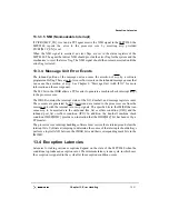
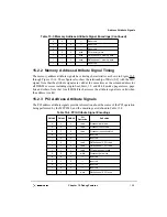
14.3 Peripheral Logic Power Management
Similar to the power management features of the processor core, the peripheral logic block
of the MPC8240 has its own doze, nap and sleep modes. They are described in the
following subsections.
The three programmable power saving modes provide different levels of power savings.
Doze, nap, and sleep are entered through software by setting the corresponding
configuration register bit in the power management control register one (PMCR1). For
more information about this register, see Section 4.3.1, “Power Management Configuration
Register 1 (PMCR1)—Offset 0x70.” In addition, the PMCR1[PM] global power
management bit must be set to 1 to enable any of the power saving modes of the peripheral
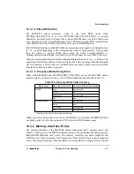
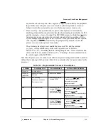
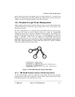
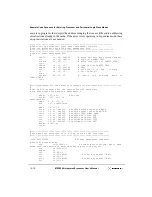
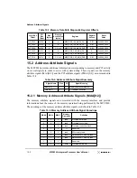
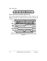
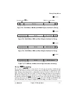
logic block. Figure 14-1 shows the four power states of the MPC8240 peripheral logic
block (three programmable power saving modes plus full-power), and the conditions
required for entering and exiting those modes.
.
Figure 14-1. MPC8240 Peripheral Logic Power States
14.3.1 MPC8240 Peripheral Power Mode Transitions
For the peripheral logic to enter into either nap or sleep mode, the processor must have
requested to enter either nap or sleep mode. If the processor wakes up from nap or sleep,
the peripheral logic also wakes up from nap or sleep.
Full
Power
Doze
Sleep
T1: PMCR1(DOZE) = 1 & PMCR1(PM) = 1
T2: hard reset, br = 0, PCI address hit, NMI
T3: PMCR1(NAP) = 1 & PMCR1(PM) = 1 & [proc_NAP (or SLEEP) request]
T4: hard reset, br = 0, PCI address hit, NMI
Nap
T5: PMCR1(SLEEP) = 1 & PMCR1(PM) = 1 & [proc_NAP (or SLEEP) request]
T6: hard reset, br = 0, NMI
T1
T2
T3
T4
T5
T6
Summary of Contents for MPC8240
Page 1: ...MPC8240UM D Rev 1 1 2001 MPC8240 Integrated Processor User s Manual ...
Page 38: ...xviii MPC8240 Integrated Processor User s Manual TABLES Table Number Title Page Number ...
Page 48: ...xlviii MPC8240 Integrated Processor User s Manual Acronyms and Abbreviations ...
Page 312: ...6 94 MPC8240 Integrated Processor User s Manual ROM Flash Interface Operation ...
Page 348: ...7 36 MPC8240 Integrated Processor User s Manual PCI Host and Agent Modes ...
Page 372: ...8 24 MPC8240 Integrated Processor User s Manual DMA Register Descriptions ...
Page 394: ...9 22 MPC8240 Integrated Processor User s Manual I2O Interface ...
Page 412: ...10 18 MPC8240 Integrated Processor User s Manual Programming Guidelines ...
Page 454: ...12 14 MPC8240 Integrated Processor User s Manual Internal Arbitration ...
Page 466: ...13 12 MPC8240 Integrated Processor User s Manual Exception Latencies ...
Page 516: ...16 14 Watchpoint Trigger Applications ...
Page 538: ...B 16 MPC8240 Integrated Processor User s Manual Setting the Endian Mode of Operation ...
Page 546: ...C 8 MPC8240 Integrated Processor User s Manual ...
Page 640: ...INDEX Index 16 MPC8240 Integrated Processor User s Manual ...