


10-4
MPC8240 Integrated Processor User’s Manual
I
2
C Protocol
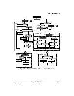
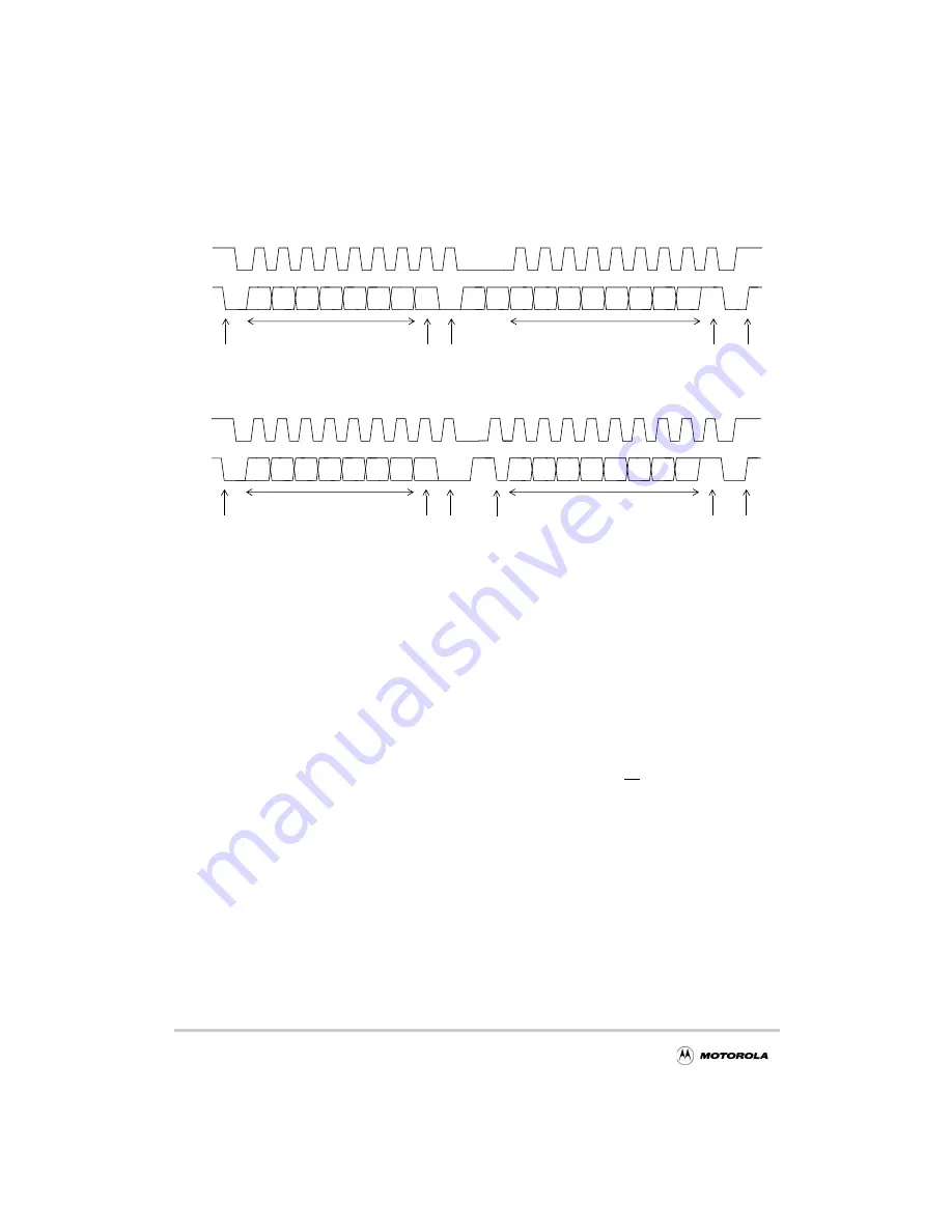
Figure 10-2. I
2
C Interface Transaction Protocol
10.2.1 START Condition
When no device is engaging the bus (both SDA and SCL lines are at logic high), a master
can initiate a transfer by sending a START condition. As shown in Figure 10-2, a
START
condition is defined as a high-to-low transition of SDA while SCL is high. This condition
denotes the beginning of a new data transfer (each data transfer can contain several bytes,
and awakens all slaves.
10.2.2 Slave Address Transmission
The first byte of data transferred by the master immediately after the START condition is
the slave address. This is a seven-bit calling address followed by a R/W bit, which indicates
the direction of the data being transferred to the slave. No two slaves in the system can have
the same address. In addition, when the I
2
C device is operating as a master, it must not
transmit an address that is the same as its slave address. An I
2
C device cannot be master and
slave at the same time.
The MPC8240 does not respond to a general call (broadcast) command unless the calling
address matches its slave address. Because general call broadcasts an address of
0b0000_000, only MPC8240s with a slave address of 0b0000_000 would respond. When
this occurs, the MPC8240 drives SDA low during the address acknowledge cycle.
Only the slave with a calling address that matches the one transmitted by the master
responds by returning an acknowledge bit (pulling the SDA signal low at the 9th clock) as
shown in Figure 10-2. If no slave acknowledges the address, the master should generate a
STOP condition or a repeated START condition.
1
2
3
4
5
6
7
8
9
1
2
3
4
5
6
7
8
9
A7
A6
A5
A4 A3
A2 A1 R/W
A7
A6
A5
A4 A3
A2 A1 R/W
D7 D6 D5 D4 D3 D2 D1
D0
XX
XX
SCL
SDA
START
STOP
ack
no
ack
read/
write
calling address
data byte
1
2
3
4
5
6
7
8
9
1
2
3
4
5
6
7
8
9
A7
A6
A5
A4 A3
A2 A1 R/W
SCL
SDA
START
STOP
ack
no
ack
read/
write
calling address
new calling address
repeat
START
Summary of Contents for MPC8240
Page 1: ...MPC8240UM D Rev 1 1 2001 MPC8240 Integrated Processor User s Manual ...
Page 38: ...xviii MPC8240 Integrated Processor User s Manual TABLES Table Number Title Page Number ...
Page 48: ...xlviii MPC8240 Integrated Processor User s Manual Acronyms and Abbreviations ...
Page 312: ...6 94 MPC8240 Integrated Processor User s Manual ROM Flash Interface Operation ...
Page 348: ...7 36 MPC8240 Integrated Processor User s Manual PCI Host and Agent Modes ...
Page 372: ...8 24 MPC8240 Integrated Processor User s Manual DMA Register Descriptions ...
Page 394: ...9 22 MPC8240 Integrated Processor User s Manual I2O Interface ...
Page 412: ...10 18 MPC8240 Integrated Processor User s Manual Programming Guidelines ...
Page 454: ...12 14 MPC8240 Integrated Processor User s Manual Internal Arbitration ...
Page 466: ...13 12 MPC8240 Integrated Processor User s Manual Exception Latencies ...
Page 516: ...16 14 Watchpoint Trigger Applications ...
Page 538: ...B 16 MPC8240 Integrated Processor User s Manual Setting the Endian Mode of Operation ...
Page 546: ...C 8 MPC8240 Integrated Processor User s Manual ...
Page 640: ...INDEX Index 16 MPC8240 Integrated Processor User s Manual ...