6-66
MPC8240 Integrated Processor User’s Manual
FPM or EDO DRAM Interface Operation
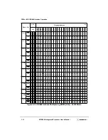
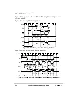
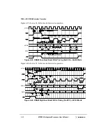
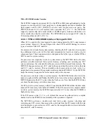
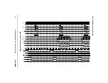
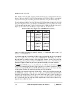
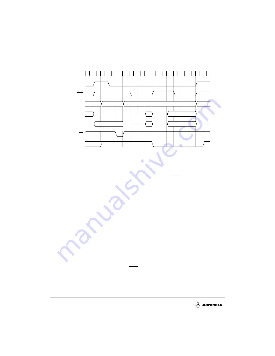
Figure 6-43 shows a single-beat write operation.
Figure 6-43. DRAM Single-Beat Write Timing with RMW or ECC Enabled
6.3.10 FPM or EDO DRAM Refresh
The MPC8240’s memory interface distributes CAS-before-RAS (CBR) refreshes to
DRAM according to the interval specified in the MCCR2[REFINT] parameter. MCCR2
must be programmed by boot code at system start-up. The value to be stored in REFINT
represents the number of memory clock cycles required between CBR refreshes.
This value should allow for a potential collision between memory access and refresh. (The
per row refresh interval should be reduced by the longest memory access time.) For
example, for a DRAM with a cell refresh time of 64 mS and 4096 rows, the per row refresh
interval would be 64 mS/4,096 rows = 15.6 µS. If the memory interface runs at 66 MHz,
15.6 µS represents 1,030 memory clock cycles. If a burst read is in progress when a refresh
is to be performed, the refresh waits for the read to complete. Thus, the per-row refresh
interval (1,030 clocks) should be reduced by the longest access time (based on
configuration parameters) and then stored to REFINT (as a binary representation of the
difference).
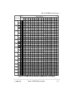
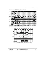
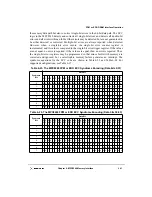
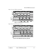
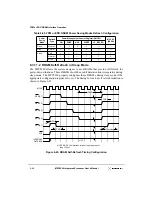
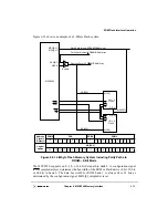
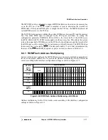
6.3.10.1 FPM or EDO Refresh Timing
The refresh timing for DRAM is controlled through MCCR3[RAS
6P
]. This register is
initialized during reset and controls the RAS active time during a CBR refresh. (Refer to
interval RAS
6P
in Figure 6-44.) As shown in the figure, the MPC8240 implements bank
staggering for CBR refreshes. System software is responsible for optimal configuration of
interval RAS
6P
after system start-up. Such configuration must be completed before
attempting access to DRAM.
MCLK
RAS
CAS
ADDR
DRAM DATA
TA
RD
ROW
COL
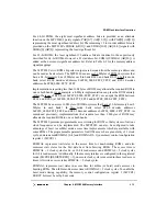
INTERNAL
DATA BUS
DRAM
MPC8240
Device driving data bus
WE
WR
RD
WR
WR
Summary of Contents for MPC8240
Page 1: ...MPC8240UM D Rev 1 1 2001 MPC8240 Integrated Processor User s Manual ...
Page 38: ...xviii MPC8240 Integrated Processor User s Manual TABLES Table Number Title Page Number ...
Page 48: ...xlviii MPC8240 Integrated Processor User s Manual Acronyms and Abbreviations ...
Page 312: ...6 94 MPC8240 Integrated Processor User s Manual ROM Flash Interface Operation ...
Page 348: ...7 36 MPC8240 Integrated Processor User s Manual PCI Host and Agent Modes ...
Page 372: ...8 24 MPC8240 Integrated Processor User s Manual DMA Register Descriptions ...
Page 394: ...9 22 MPC8240 Integrated Processor User s Manual I2O Interface ...
Page 412: ...10 18 MPC8240 Integrated Processor User s Manual Programming Guidelines ...
Page 454: ...12 14 MPC8240 Integrated Processor User s Manual Internal Arbitration ...
Page 466: ...13 12 MPC8240 Integrated Processor User s Manual Exception Latencies ...
Page 516: ...16 14 Watchpoint Trigger Applications ...
Page 538: ...B 16 MPC8240 Integrated Processor User s Manual Setting the Endian Mode of Operation ...
Page 546: ...C 8 MPC8240 Integrated Processor User s Manual ...
Page 640: ...INDEX Index 16 MPC8240 Integrated Processor User s Manual ...