

Chapter 5. PowerPC Processor Core
5-9
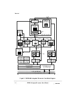
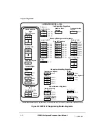
PowerPC Processor Core Features
The MMUs translate effective addresses and enforce the protection hierarchy programmed
by the operating system in relation to the supervisor/user privilege level of the access and
in relation to the type of access—load or store.
5.2.6.2 Cache Units
The processor core provides independent 16-Kbyte, four-way set-associative instruction
and data caches. The cache block size is 32 bytes. The caches are designed to adhere to a
write-back policy, but the processor core allows control of cacheability, write policy, and
memory coherency at the page and block levels. The caches use a least recently used (LRU)
replacement algorithm.
The load/store and instruction fetch units provide the caches with the address of the data or
instruction to be fetched. In the case of a cache hit, the cache returns two words to the
requesting unit.
Note that the MPC8240 processor core has some additional cache locking functionality
compared to the MPC603e. This is described in more detail in Section 5.4.2.3, “Cache
Locking.”
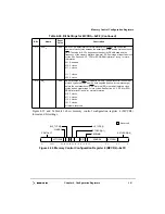
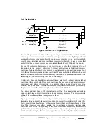
5.2.6.3 Peripheral Logic Bus Interface
The MPC8240 contains an internal peripheral logic bus that interfaces the processor core
to the peripheral logic. This internal bus is very similar in function to the external 60x bus
interface on the MPC603e. In the case of the MPC8240, the central control unit (CCU)
terminates all the transactions and internally directs all accesses to the appropriate
peripheral (or memory) interface.
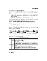
5.2.6.3.1 Peripheral Logic Bus Protocol
The processor core-to-peripheral logic interface includes a 32-bit address bus, a 32- or
64-bit data bus as well as control and information signals. The peripheral logic interface
allows for address-only transactions as well as address and data transactions. The processor
core control and information signals include the address arbitration, address start, address
transfer, transfer attribute, address termination, data arbitration, data transfer, data
termination, and processor state signals. Test and control signals provide diagnostics for
selected internal circuits.
The peripheral logic interface supports bus pipelining, which allows the address tenure of
one transaction to overlap the data tenure of another. PCI accesses to the memory space are
monitored by the peripheral logic bus to allow the processor to snoop these accesses
(provided PICR[27] is cleared).
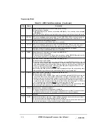
5.2.6.3.2 Peripheral Logic Bus Data Transfers
As part of the peripheral logic bus interface, the processor core’s data bus is configured at
power-up (by the value on the MDL[0] signal) to either a 32- or 64-bit width.
Summary of Contents for MPC8240
Page 1: ...MPC8240UM D Rev 1 1 2001 MPC8240 Integrated Processor User s Manual ...
Page 38: ...xviii MPC8240 Integrated Processor User s Manual TABLES Table Number Title Page Number ...
Page 48: ...xlviii MPC8240 Integrated Processor User s Manual Acronyms and Abbreviations ...
Page 312: ...6 94 MPC8240 Integrated Processor User s Manual ROM Flash Interface Operation ...
Page 348: ...7 36 MPC8240 Integrated Processor User s Manual PCI Host and Agent Modes ...
Page 372: ...8 24 MPC8240 Integrated Processor User s Manual DMA Register Descriptions ...
Page 394: ...9 22 MPC8240 Integrated Processor User s Manual I2O Interface ...
Page 412: ...10 18 MPC8240 Integrated Processor User s Manual Programming Guidelines ...
Page 454: ...12 14 MPC8240 Integrated Processor User s Manual Internal Arbitration ...
Page 466: ...13 12 MPC8240 Integrated Processor User s Manual Exception Latencies ...
Page 516: ...16 14 Watchpoint Trigger Applications ...
Page 538: ...B 16 MPC8240 Integrated Processor User s Manual Setting the Endian Mode of Operation ...
Page 546: ...C 8 MPC8240 Integrated Processor User s Manual ...
Page 640: ...INDEX Index 16 MPC8240 Integrated Processor User s Manual ...