

Chapter 4. Configuration Registers
4-49
Memory Control Configuration Registers
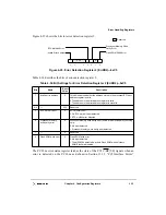
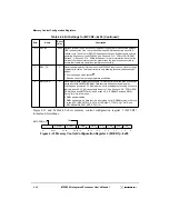
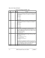
Table 4-40. Bit Settings for MCCR3—0xF8
Bits
Name
Reset
Value
Description
31–28
BSTOPRE[2–5]
0000
Burst to precharge—bits 2–5. For SDRAM only. These bits, together with
BSTOPRE[0–1] (bits 19–18 of MCCR4), and BSTOPRE[6–9] (bits 3–0 of
MCCR4), control the open page interval. The page open duration counter is
reloaded with BSTOPRE[0–9] every time the page is accessed (including page
hits). When the counter expires, the open page is closed with a
SDRAM-precharge bank command. Section 6.2.7, “SDRAM Page Mode,” for
more information.
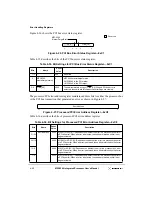
27–24
REFREC
0000
Refresh to activate interval. For SDRAM only. These bits control the number of
clock cycles from an SDRAM-refresh command until an SDRAM-activate
command is allowed. See Section 6.2.12, “SDRAM Refresh,” for more
information.
0001 1 clock
0010 2 clocks
0011 3 clocks
...
...
1111 15 clocks
0000 16 clocks
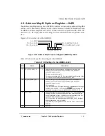
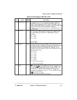
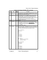
23–20
RDLAT
0000
Data latency from read command. For SDRAM only. These bits control the
number of clock cycles from an SDRAM-read command until the first data beat
is available on the data bus. RDLAT values greater than 6 clocks are not
supported. See Section 6.2.4, “SDRAM Power-On Initialization,” for more
information. Note that for SDRAM, this value must be programmed to a valid
value (from the reset value).
0000 Reserved
0001 1 clock
0010 2 clocks
0011 3 clocks
0100 4 clocks
0101 5 clocks
0110 6 clocks
0111 Reserved (not supported)
...
...
1111 Reserved (not supported)
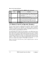
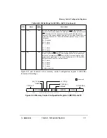
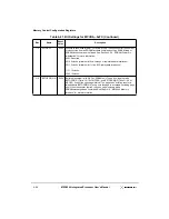
19
CPX
0
CAS write timing modifier. For DRAM/EDO only. When set, this bit adds one
clock cycle to the CAS precharge interval (CP
4
+ 1) and subtracts one clock
cycle from the CAS assertion interval for page mode access (CAS
5
- 1) for
write operations to DRAM/EDO. Note that this requires CAS
5
> 2. Read
operations are unmodified. See Section 6.3.5, “FPM or EDO DRAM Interface
Timing,” for more information.
0 CAS write timing is unmodified
1 CAS write timing is modified as described above
Summary of Contents for MPC8240
Page 1: ...MPC8240UM D Rev 1 1 2001 MPC8240 Integrated Processor User s Manual ...
Page 38: ...xviii MPC8240 Integrated Processor User s Manual TABLES Table Number Title Page Number ...
Page 48: ...xlviii MPC8240 Integrated Processor User s Manual Acronyms and Abbreviations ...
Page 312: ...6 94 MPC8240 Integrated Processor User s Manual ROM Flash Interface Operation ...
Page 348: ...7 36 MPC8240 Integrated Processor User s Manual PCI Host and Agent Modes ...
Page 372: ...8 24 MPC8240 Integrated Processor User s Manual DMA Register Descriptions ...
Page 394: ...9 22 MPC8240 Integrated Processor User s Manual I2O Interface ...
Page 412: ...10 18 MPC8240 Integrated Processor User s Manual Programming Guidelines ...
Page 454: ...12 14 MPC8240 Integrated Processor User s Manual Internal Arbitration ...
Page 466: ...13 12 MPC8240 Integrated Processor User s Manual Exception Latencies ...
Page 516: ...16 14 Watchpoint Trigger Applications ...
Page 538: ...B 16 MPC8240 Integrated Processor User s Manual Setting the Endian Mode of Operation ...
Page 546: ...C 8 MPC8240 Integrated Processor User s Manual ...
Page 640: ...INDEX Index 16 MPC8240 Integrated Processor User s Manual ...