
2-32
MPC8240 Integrated Processor User’s Manual
Detailed Signal Descriptions
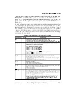
2.2.6.3 JTAG Test Data Input (TDI)—Input
Following is the state meaning for the TDI input signal.
State Meaning
Asserted/Negated—The value presented on this signal on the rising
edge of TCK is clocked into the selected JTAG test instruction or
data register.
Note that this input contains an internal pull-up resistor to ensure that
an unterminated input appears as a high signal level to the test logic.
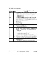
2.2.6.4 JTAG Test Data Output (TDO)—Output
Following is the state meaning for the TDO output signal.
State Meaning
Asserted/Negated—The contents of the selected internal instruction
or data register are shifted out onto this signal on the falling edge of
TCK. The TDO signal remains in a high-impedance state except
when scanning of data is in progress.
2.2.6.5 JTAG Test Mode Select (TMS)—Input
The test mode select (TMS) signal is an input on the MPC8240. Following is the state
meaning for the TMS input signal.
State Meaning
Asserted/Negated—This signal is decoded by the internal JTAG TAP
controller to distinguish the primary operation of the test support
circuitry.
Note that this input contains an internal pull-up resistor to ensure that
an unterminated input appears as a high signal level to the test logic.
2.2.6.6 JTAG Test Reset (TRST)—Input
The test reset (TRST) signal is an input on the MPC8240. Following is the state meaning
for the TRST input signal.
State Meaning
Asserted—This input causes asynchronous initialization of the
internal JTAG test access port controller. Note that the signal must be
asserted during power-up reset in order to initialize properly the
JTAG test access port.
Negated—Indicates normal operation.
Note that this input contains an internal pull-up resistor to ensure that
an unterminated input appears as a high signal level to the test logic.
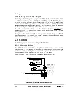
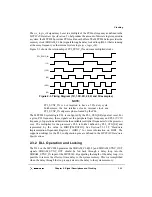
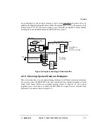
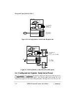
2.2.7 Clock Signals
The MPC8240 coordinates clocking across the memory bus and the PCI bus. This section
provides a brief description of the MPC8240 clock signals. See Section 2.3, “Clocking,” for
more detailed information on the use of the MPC8240 clock signals.
Summary of Contents for MPC8240
Page 1: ...MPC8240UM D Rev 1 1 2001 MPC8240 Integrated Processor User s Manual ...
Page 38: ...xviii MPC8240 Integrated Processor User s Manual TABLES Table Number Title Page Number ...
Page 48: ...xlviii MPC8240 Integrated Processor User s Manual Acronyms and Abbreviations ...
Page 312: ...6 94 MPC8240 Integrated Processor User s Manual ROM Flash Interface Operation ...
Page 348: ...7 36 MPC8240 Integrated Processor User s Manual PCI Host and Agent Modes ...
Page 372: ...8 24 MPC8240 Integrated Processor User s Manual DMA Register Descriptions ...
Page 394: ...9 22 MPC8240 Integrated Processor User s Manual I2O Interface ...
Page 412: ...10 18 MPC8240 Integrated Processor User s Manual Programming Guidelines ...
Page 454: ...12 14 MPC8240 Integrated Processor User s Manual Internal Arbitration ...
Page 466: ...13 12 MPC8240 Integrated Processor User s Manual Exception Latencies ...
Page 516: ...16 14 Watchpoint Trigger Applications ...
Page 538: ...B 16 MPC8240 Integrated Processor User s Manual Setting the Endian Mode of Operation ...
Page 546: ...C 8 MPC8240 Integrated Processor User s Manual ...
Page 640: ...INDEX Index 16 MPC8240 Integrated Processor User s Manual ...