
2-30
MPC8240 Integrated Processor User’s Manual
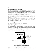
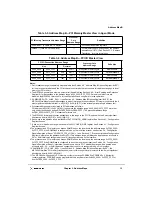
Detailed Signal Descriptions
2.2.5.10.1 Memory Address Attributes (MAA[0:2])—Output
The memory attribute signals are associated with the memory interface and provide
information about the source of the memory operation being performed by the MPC8240.
They are also reset configuration input signals.
State Meaning
Asserted/Negated—These signals are encoded to provide more
detailed information about a memory transaction. See
Section 15.2.1, “Memory Address Attribute Signals (MAA[0:2]),”
for a table showing these encodings.
Timing Comments
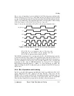
Assertion/Negation—Section 15.2.2, “Memory Address Attribute
Signal Timing,” refers to timing diagrams showing the relative
timing of these signals and the rest of the memory interface.
2.2.5.10.2 PCI Address Attributes (PMAA[0:2])—Output
The memory attribute signals are associated with the PCI interface and provide information
about the source of the PCI operation being performed by the MPC8240. They are also reset
configuration input signals.
State Meaning
Asserted/Negated—These signals are encoded to provide more
detailed information about a PCI transaction. See Section 15.2.3,
“PCI Address Attribute Signals,” for a table showing these
encodings.
Timing Comments
Assertion/Negation—Section 15.2.4, “PCI Address Attribute Signal
Timing,” contains timing diagrams showing the relative timing of
these signals and the rest of the PCI interface.
2.2.5.10.3 Debug Address (DA[0:15])—Output
When enabled, the debug address provides software disassemblers a simple way to
reconstruct the 30-bit physical address for a memory bus transaction to DRAM and
SDRAM, ROM, Flash, or PortX. Note that most of these signals are multiplexed with other
signals (that may be inputs in their alternate function).
State Meaning
Asserted/Negated—Section 15.3, “Memory Debug Address,”
describes these signals in detail, and how they are mapped to
different address bits, depending on the type of memory in use.
Timing Comments
Assertion/Negation— For DRAM or SDRAM, these 16 debug
address signals are sampled with the column address and
chip-selects. For ROM, Flash, and PortX devices, the debug address
pins are sampled at the same time as the ROM address and can be
used to recreate the 24-bit physical address in conjunction with ROM
address.
Summary of Contents for MPC8240
Page 1: ...MPC8240UM D Rev 1 1 2001 MPC8240 Integrated Processor User s Manual ...
Page 38: ...xviii MPC8240 Integrated Processor User s Manual TABLES Table Number Title Page Number ...
Page 48: ...xlviii MPC8240 Integrated Processor User s Manual Acronyms and Abbreviations ...
Page 312: ...6 94 MPC8240 Integrated Processor User s Manual ROM Flash Interface Operation ...
Page 348: ...7 36 MPC8240 Integrated Processor User s Manual PCI Host and Agent Modes ...
Page 372: ...8 24 MPC8240 Integrated Processor User s Manual DMA Register Descriptions ...
Page 394: ...9 22 MPC8240 Integrated Processor User s Manual I2O Interface ...
Page 412: ...10 18 MPC8240 Integrated Processor User s Manual Programming Guidelines ...
Page 454: ...12 14 MPC8240 Integrated Processor User s Manual Internal Arbitration ...
Page 466: ...13 12 MPC8240 Integrated Processor User s Manual Exception Latencies ...
Page 516: ...16 14 Watchpoint Trigger Applications ...
Page 538: ...B 16 MPC8240 Integrated Processor User s Manual Setting the Endian Mode of Operation ...
Page 546: ...C 8 MPC8240 Integrated Processor User s Manual ...
Page 640: ...INDEX Index 16 MPC8240 Integrated Processor User s Manual ...