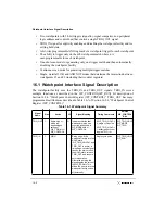

16-8
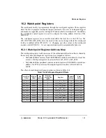
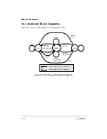
Watchpoint Registers
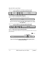
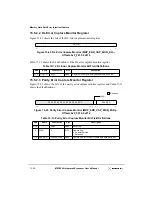
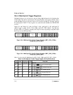
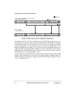
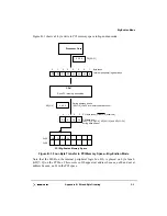
Figure 16-9 and Figure 16-10 show the format of the watchpoint #1 and watchpoint #2
address mask registers (WP1_ADDR_MASK and WP2_ADDR_MASK). The format is
identical, but they are shown separately to show the offsets.
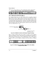
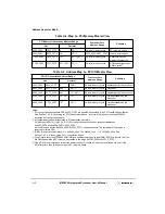
Figure 16-9. Watchpoint #1 Address Mask Register (WP1_ADDR_MASK)—
Offsets 0xF_F024, 0xF24
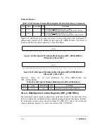
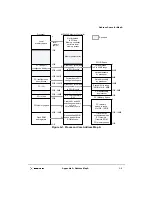
Figure 16-10. Watchpoint #2 Address Mask Register (WP2_ADDR_MASK)—
Offsets 0xF_F03C, 0xF3C
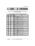
16-6 shows the bit field definitions for WP1_ADDR_MASK and
WP2_ADDR_MASK.
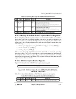
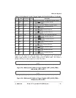
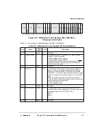
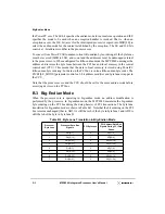
16.2.4 Watchpoint Control Register (WP_CONTROL)
The watchpoint control register configures the watchpoint facility. It has fields that allow
the user to enable the watchpoint facility, enable the debug addresses in software, initialize
the watchpoint counters, select the driver modes for TRIG_OUT, and set the watchpoint
mode of operation. Figure 16-11 shows the format of WP_CONTROL.
1
INT_
0
R/W
0 Ignore INT_ trigger bit in WPx_CNTL_TRIG.
1 Compare INT on peripheral logic bus with WPx_CNTL_TRIG bit.
0
MCP_
0
R/W
0 Ignore MCP_ trigger bit in WPx_CNTL_TRIG.
1 Compare MCP on peripheral logic bus with WPx_CNTL_TRIG bit.
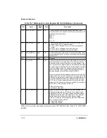
Table 16-6. Watchpoint Address Mask Register Bit Field Definitions
Bits
Name
Reset Value
R/W
Description
31–0
A[31:0]
all 0s
R/W
Trigger mask for peripheral logic address bus
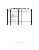
Table 16-5. Watchpoint Control Mask Register Bit Field Definitions (Continued)
Bits
Name
Reset Value
R/W
Description
A[31:0]
31 30 29 28 27 26 25
24
23
22
21
20
19
18
17
16
15
14
13
12
11
10
9
8
7
6
5
4
3
2
1
0
A[31:0]
31 30 29 28 27 26 25
24
23
22
21
20
19
18
17
16
15
14
13
12
11
10
9
8
7
6
5
4
3
2
1
0
Summary of Contents for MPC8240
Page 1: ...MPC8240UM D Rev 1 1 2001 MPC8240 Integrated Processor User s Manual ...
Page 38: ...xviii MPC8240 Integrated Processor User s Manual TABLES Table Number Title Page Number ...
Page 48: ...xlviii MPC8240 Integrated Processor User s Manual Acronyms and Abbreviations ...
Page 312: ...6 94 MPC8240 Integrated Processor User s Manual ROM Flash Interface Operation ...
Page 348: ...7 36 MPC8240 Integrated Processor User s Manual PCI Host and Agent Modes ...
Page 372: ...8 24 MPC8240 Integrated Processor User s Manual DMA Register Descriptions ...
Page 394: ...9 22 MPC8240 Integrated Processor User s Manual I2O Interface ...
Page 412: ...10 18 MPC8240 Integrated Processor User s Manual Programming Guidelines ...
Page 454: ...12 14 MPC8240 Integrated Processor User s Manual Internal Arbitration ...
Page 466: ...13 12 MPC8240 Integrated Processor User s Manual Exception Latencies ...
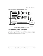
Page 516: ...16 14 Watchpoint Trigger Applications ...
Page 538: ...B 16 MPC8240 Integrated Processor User s Manual Setting the Endian Mode of Operation ...
Page 546: ...C 8 MPC8240 Integrated Processor User s Manual ...
Page 640: ...INDEX Index 16 MPC8240 Integrated Processor User s Manual ...