
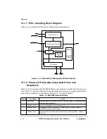

Chapter 12. Central Control Unit
12-5
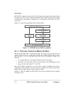
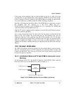
Internal Buffers
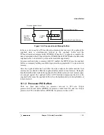
The PCI interface of the MPC8240 continues to request mastership of the PCI bus until the
processor’s original request is completed. When the next processor transaction starts, the
address is snooped against the address of the previous transaction (in the internal address
buffer) to verify that the same cache line is being requested. Once all the requested data is
latched, and all PCI write to local memory snoops have completed, the CCU completes the
data transfer to the processor.
For example, if the processor initiates a critical-word-first burst read, starting with the
second double word of a cache line, the read on the PCI bus begins with the
cache-line-aligned address. If the PCI target disconnects after transferring the first half of
the cache line, the MPC8240 re-arbitrates for the PCI bus, and when granted, initiates a new
transaction with the address of the third double word of the line. If an alternate PCI master
requests data from local memory while the MPC8240 is waiting for the PCI bus grant, the
central control unit internally retries the processor core transaction to allow the
PCI-initiated transaction to be snooped by the processor core. When the processor snoop is
complete, the subsequent processor transaction is compared to the latched address and
attributes of the PRPRB to ensure that the processor is requesting data for the same cache
line. After all data requested by the processor is latched in the PRPRB, the data is
transferred to the processor, completing the transaction.
12.1.2.2 Processor-to-PCI-Write Buffers (PRPWBs)
There are two 16-byte buffers for processor writes to PCI. These buffers can be used
together as one 32-byte buffer for processor burst writes to PCI or separately for single-beat
writes to PCI. This allows the MPC8240 to support both burst transactions and streams of
single-beat transactions. The MPC8240 performs store gathering (if enabled) of sequential
accesses within the 16-byte range that comprises either the first or second half of the cache
line. All transfer sizes are gathered if enabled (PICR1[ST_GATH_EN] = 1).
The internal buffering minimizes the effect of the slower PCI bus on the higher-speed
peripheral logic bus that interfaces to the processor core. After the processor write data is
latched internally, the internal peripheral logic bus is available for subsequent transactions,
and it doesn’t need to wait for the write to the PCI target to complete. Note that both PCI
memory and I/O accesses are buffered. Device drivers must take into account that writes to
I/O devices on the PCI bus are posted. The processor may believe that the write has
completed while the MPC8240 is still trying to acquire mastership of the PCI bus.
If the processor core initiates a burst write to PCI, the processor data transfer is delayed
until all previous writes to PCI are completed, and then the burst data from the processor
fills the two PRPWBs. The address and transfer attributes are stored in the first address
buffer.
For a stream of single-beat writes, the data for the first transaction is latched in the first
buffer and the MPC8240 initiates the transaction on the PCI bus. The second single-beat
write is then stored in the second buffer. For subsequent single-beat writes, store gathering
is possible if the incoming write is to sequential bytes in the same half cache line as the
Summary of Contents for MPC8240
Page 1: ...MPC8240UM D Rev 1 1 2001 MPC8240 Integrated Processor User s Manual ...
Page 38: ...xviii MPC8240 Integrated Processor User s Manual TABLES Table Number Title Page Number ...
Page 48: ...xlviii MPC8240 Integrated Processor User s Manual Acronyms and Abbreviations ...
Page 312: ...6 94 MPC8240 Integrated Processor User s Manual ROM Flash Interface Operation ...
Page 348: ...7 36 MPC8240 Integrated Processor User s Manual PCI Host and Agent Modes ...
Page 372: ...8 24 MPC8240 Integrated Processor User s Manual DMA Register Descriptions ...
Page 394: ...9 22 MPC8240 Integrated Processor User s Manual I2O Interface ...
Page 412: ...10 18 MPC8240 Integrated Processor User s Manual Programming Guidelines ...
Page 454: ...12 14 MPC8240 Integrated Processor User s Manual Internal Arbitration ...
Page 466: ...13 12 MPC8240 Integrated Processor User s Manual Exception Latencies ...
Page 516: ...16 14 Watchpoint Trigger Applications ...
Page 538: ...B 16 MPC8240 Integrated Processor User s Manual Setting the Endian Mode of Operation ...
Page 546: ...C 8 MPC8240 Integrated Processor User s Manual ...
Page 640: ...INDEX Index 16 MPC8240 Integrated Processor User s Manual ...