

Chapter 6. MPC8240 Memory Interface
6-79
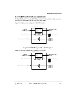
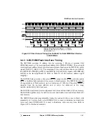
ROM/Flash Interface Operation
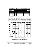
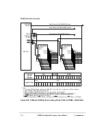
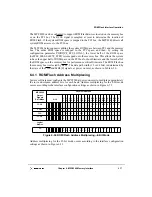
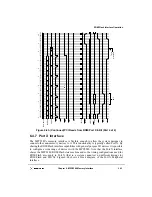
For 64-bit ROMs, the eight most significant address bits are provided as an alternate
function on the MPC8240’s parity signals, PAR[0:7] (AR[19:12]), with PAR[0] (AR[19])
representing the most significant address bit. The remaining 12 low-order address bits are
provided on the MPC8240’s SDBA0 (AR[11]) and SDMA[10:0] (AR[10:0]) signals with
SDMA[0] (AR[0]) representing the least significant bit.
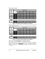
For 32-bit ROMs, the least significant 20 address bits are identical to those previously
described for 64-bit ROMs. However, a 21st address bit, SDMA12/SDBA1 (AR[20]), is
added as the new most significant address bit. Refer to Table 6-2 for the memory address
signal mappings.
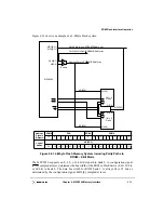
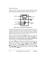
The MPC8240’s two ROM chip select outputs are decoded from the memory address and
can be used as bank selects. The MPC8240 can access 16 Mbytes of ROM in systems that
have a 64-bit memory bus (8 Mbytes each in bank RSC0 and bank RSC1). In this mode,
bank select RCS0 decodes addresses 0xFF80_0000–FFFF_FFFF, and RCS1 decodes
addresses 0xFF00_0000–FF7F_FFFF.
Implementations requiring less than 16 Mbytes of ROM may allocate the required ROM to
one or both banks. As an example, a 4-Mbyte implementation can place the ROM entirely
within the range of RCS0, (at 0xFFC0_0000–FFFF_FFFF), or can split the ROM between
RCS1 and RCS0, (at 0xFF60_0000–FF7F_FFFF and 0xFFE0_0000–FFFF_FFFF).
The MPC8240 can access 16 Mbytes of ROM in systems that have a 32-bit memory bus (8
Mbytes in each bank). In this mode, bank select RCS0 decodes addresses
0xFF80_0000–FFFF_FFFF, and RCS1 decodes addresses 0xFF00_0000–FF7F_FFFF. As
mentioned previously, implementations that require less than 8 Mbytes of ROM may
allocate the required ROM to one or both banks.
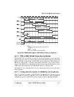
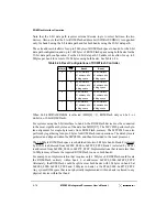
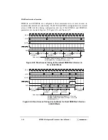
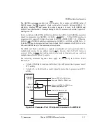
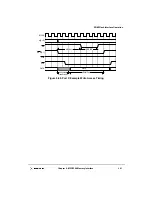
The MPC8240 provides programmable access timing for ROM so that systems of various
clock frequencies can be implemented. The MPC8240 can also be configured to take
advantage of burst (or nibble) mode access time improvements which are available with
some ROMs. The programmable parameters for ROM access have granularity of 1 clock
cycle, and are named ROMFAL[0–4] and ROMNAL[0–3] in memory control configuration
register 1 (MCCR1).
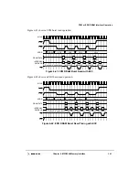
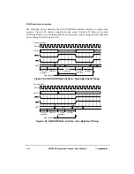
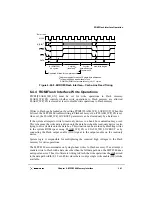
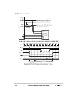
ROMFAL represents wait states in the access time for non-bursting ROMs, and also
measures wait states for the first data beat from bursting ROMs. The access time is
3 clock cycles for 64- or 32-bit read accesses and 2 clock cycles
for 8-bit read accesses. Additionally, if the memory interface is configured in the registered
mode (MCCR4[REGISTERED] = 1], one more clock cycle is incurred in these read access
times. All write accesses takes 2 clock cycles.
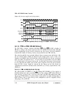
ROMNAL represents wait states in access time for nibble (or burst) mode accesses to
bursting ROMs. The nibble mode access time is 2 clock cycles. To enable the
burst mode timing capability, the memory control configuration register 1 (MCCR1)
BURST bit must be set by boot code.
Summary of Contents for MPC8240
Page 1: ...MPC8240UM D Rev 1 1 2001 MPC8240 Integrated Processor User s Manual ...
Page 38: ...xviii MPC8240 Integrated Processor User s Manual TABLES Table Number Title Page Number ...
Page 48: ...xlviii MPC8240 Integrated Processor User s Manual Acronyms and Abbreviations ...
Page 312: ...6 94 MPC8240 Integrated Processor User s Manual ROM Flash Interface Operation ...
Page 348: ...7 36 MPC8240 Integrated Processor User s Manual PCI Host and Agent Modes ...
Page 372: ...8 24 MPC8240 Integrated Processor User s Manual DMA Register Descriptions ...
Page 394: ...9 22 MPC8240 Integrated Processor User s Manual I2O Interface ...
Page 412: ...10 18 MPC8240 Integrated Processor User s Manual Programming Guidelines ...
Page 454: ...12 14 MPC8240 Integrated Processor User s Manual Internal Arbitration ...
Page 466: ...13 12 MPC8240 Integrated Processor User s Manual Exception Latencies ...
Page 516: ...16 14 Watchpoint Trigger Applications ...
Page 538: ...B 16 MPC8240 Integrated Processor User s Manual Setting the Endian Mode of Operation ...
Page 546: ...C 8 MPC8240 Integrated Processor User s Manual ...
Page 640: ...INDEX Index 16 MPC8240 Integrated Processor User s Manual ...