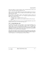


Chapter 5. PowerPC Processor Core
5-21
Cache Implementation
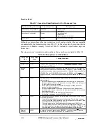
PowerPC microprocessors control the following memory access modes on a page or block
basis:
•
Write-back/write-through mode
•
Caching-inhibited mode
•
Memory coherency
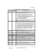
The PowerPC cache management instructions provide a means by which the application
programmer can affect the cache contents.
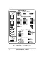
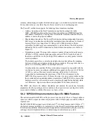
5.4.2 MPC8240 Implementation-Specific Cache
Implementation
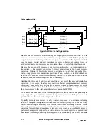
As shown in Figure 5-1, the caches provide a 64-bit interface to the instruction fetch unit
and load/store unit. The surrounding logic selects, organizes, and forwards the requested
information to the requesting unit. Write operations to the cache can be performed on a byte
basis, and a complete read-modify-write operation to the cache can occur in each cycle.
Each cache block contains eight contiguous words from memory that are loaded from an
8-word boundary (that is, bits A27–A31 of the effective addresses are zero); thus, a cache
block never crosses a page boundary. Misaligned accesses across a page boundary can incur
a performance penalty.
The cache blocks are loaded in to the processor core in four beats of 64 bits each. The burst
load is performed as critical double word first.
To ensure coherency among caches in a multiprocessor (or multiple caching-device)
implementation, the processor core implements the MEI protocol. These three states,
modified, exclusive, and invalid, indicate the state of the cache block as follows:
•
Modified—The cache block is modified with respect to system memory; that is, data
for this address is valid only in the cache and not in system memory.
•
Exclusive—This cache block holds valid data that is identical to the data at this
address in system memory. No other cache has this data.
•
Invalid—This cache block does not hold valid data.
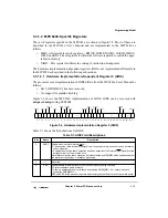
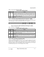
5.4.2.1 Data Cache
As shown in Figure 5-6, the data cache is configured as 128 sets of four blocks each. Each
block consists of 32 bytes, two state bits, and an address tag. The two state bits implement
the three-state MEI (modified/exclusive/invalid) protocol. Each block contains eight 32-bit
words. Note that the PowerPC architecture defines the term ‘block’ as the cacheable unit.
For the MPC8240’s processor core, the block size is equivalent to a cache line.
Summary of Contents for MPC8240
Page 1: ...MPC8240UM D Rev 1 1 2001 MPC8240 Integrated Processor User s Manual ...
Page 38: ...xviii MPC8240 Integrated Processor User s Manual TABLES Table Number Title Page Number ...
Page 48: ...xlviii MPC8240 Integrated Processor User s Manual Acronyms and Abbreviations ...
Page 312: ...6 94 MPC8240 Integrated Processor User s Manual ROM Flash Interface Operation ...
Page 348: ...7 36 MPC8240 Integrated Processor User s Manual PCI Host and Agent Modes ...
Page 372: ...8 24 MPC8240 Integrated Processor User s Manual DMA Register Descriptions ...
Page 394: ...9 22 MPC8240 Integrated Processor User s Manual I2O Interface ...
Page 412: ...10 18 MPC8240 Integrated Processor User s Manual Programming Guidelines ...
Page 454: ...12 14 MPC8240 Integrated Processor User s Manual Internal Arbitration ...
Page 466: ...13 12 MPC8240 Integrated Processor User s Manual Exception Latencies ...
Page 516: ...16 14 Watchpoint Trigger Applications ...
Page 538: ...B 16 MPC8240 Integrated Processor User s Manual Setting the Endian Mode of Operation ...
Page 546: ...C 8 MPC8240 Integrated Processor User s Manual ...
Page 640: ...INDEX Index 16 MPC8240 Integrated Processor User s Manual ...