MITWELL PSMC-C301 User’s Guide (Official R2.0)
Copyright © MITWELL 2017 PSMC-C301 User's Guide
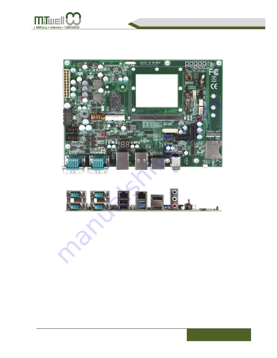
1
PSMC-C301
SMARC 2.0 compliant
Mitwell Evaluation Board
Revision 2.0
Page 1: ...MITWELL PSMC C301 User s Guide Official R2 0 Copyright MITWELL 2017 PSMC C301 User s Guide 1 PSMC C301 SMARC 2 0 compliant Mitwell Evaluation Board Revision 2 0...
Page 2: ...s Guide Official R2 0 Copyright MITWELL 2017 PSMC C301 User s Guide 2 Revision History Ver Description Date Approved R1 0 Initial release 2017 07 26 Penny Chiang R2 0 Design stepping from R0 to R1 20...
Page 3: ...2 1 ATX AT Power supply mode 11 3 2 2 Power Status LEDs D30 D31 D32 11 4 Connector Subsystem 12 4 1 SMARC Edge Finger Pinout Circuit 12 4 2 Communication Buses 14 4 2 1 CAN BUS 14 4 2 2 Serial Ports...
Page 4: ...consequential damages caused by the use or misuse of or inability to use the MITWELL products regardless of the legal theory on which the claim is based and even if MITWELL has been advised of the po...
Page 5: ...away from water or liquid sources Keep the board away from high heat or high humidity Keep the board properly ventilated do not block or cover ventilation openings Make sure to use recommended voltage...
Page 6: ...15W are possible Two Module sizes are defined 82mm x 50mm and 82mm x 80mm The Module PCBs have 314 edge fingers that mate with a low profile 314 pin 0 5mm pitch right angle connector the connector is...
Page 7: ...ELL s SMARC 2 0 compliant carrier board PSMC C301 By providing detail schematic and functional design information in this manual the PSMC C301 carrier board provides manufactures and developers with a...
Page 8: ...Px2 P 1 25mm 180D 4 Wall LVDS J65 M 2 KEY E J67 MiniPCI Express J69 FPC 24P P 1 0mm 90D CSI1 J72 SD Card H 2 75mm SD Slot J73 Pin Header 7Px2 P 2 0mm 180D ESPI J78 PCIe x1_36Pin J79 RJ45 USB3 0x2 J81...
Page 9: ...ficial R2 0 Copyright MITWELL 2017 PSMC C301 User s Guide 9 JP24 PH3Px2 LVDS1 Backlight Select JP36 PH3Px1 RTC Select JP38 HEADER3P 2mm I2S_Audio Line_IN Line_OUT MIC_JD JP39 HEADER3P 2mm M 2 Micro US...
Page 10: ...01 carrier board supports standard 20 pin ATX power supply J54 and 9V 36V DC variable power supply via pheonix connector J71 JP54 Standard 20 pin ATX Connector 20P The PSMC C301 used with standard ATX...
Page 11: ...when you turn on the power supply Configure the power supply to ATX or AT mode with Jumper JP14 JP14 Header3Px1 2 54mm ATX AT Mode Select Function Signal Description Figure 1 2 ATX Mode Default 2 3 A...
Page 12: ...MITWELL PSMC C301 User s Guide Official R2 0 Copyright MITWELL 2017 PSMC C301 User s Guide 12 4 Connector Subsystem 4 1 SMARC Edge Finger Pinout Circuit...
Page 13: ...MITWELL PSMC C301 User s Guide Official R2 0 Copyright MITWELL 2017 PSMC C301 User s Guide 13...
Page 14: ...C301 features two CAN BUS over DB9 connector type for product with CAN BUS features CAN BUS is Not Supported by PSMC M1011 J56A D SUB 9Px2 CAN0 PIN No Signal Description Figure 1 NC 2 CAN0L 3 GND 4 N...
Page 15: ...x Header 5Px2 P 2 54mm at J59 COM1 and COM3 port may be selected to support RS232 RS422 RS485 via different jumper setting J57A D SUB 9Px2 COM1 PIN No Signal Description Figure 1 485D 422T 2 RS232RX D...
Page 16: ...NC 2 COM_RX 2 3 COM_TX 2 4 NC 5 GND 6 NC 7 NC 8 NC 9 NC 10 NC J57B D SUB 9Px2 COM3 PIN No Signal Description Figure 1 485D 422T 1 2 RS232RX DT 1 3 RS232TX 422R 1 4 422R 1 5 GND 6 NC 7 RS232RTS1 8 RS23...
Page 17: ...al Description Figure 1 NC 2 COM_RX 21 3 COM_TX 21 4 NC 5 GND 6 NC 7 NC 8 NC 9 NC 10 NC 4 2 3 Gigabit Ethernet GbE and USB PSMC C301 provides two Gigabit Ethernet over RJ45 connectors with transformer...
Page 18: ...gure A1 Power VBUS_5 A2 USB5 _P A3 USB5 _P A4 GND B1 Power VBUS_1 B2 USB1 _P B3 USB1 _P B4 GND C1 Power GBE0_CTREF C2 GBE0_MDI0 C3 GBE0_MDI0 C4 GBE0_MDI1 C5 GBE0_MDI1 C6 GBE0_MDI2 C7 GBE0_MDI2 C8 GBE0...
Page 19: ...BUS_2 A2 USB2 _P A3 USB2 _P A4 GND A5 USB2_SSRX _P A6 USB2_SSRX _P A7 GND A8 USB2_SSTX _P A9 USB2_SSTX _P B1 Power VBUS_3 B2 USB3 _P B3 USB3 _P B4 GND B5 USB3_SSRX _P B6 USB3_SSRX _P B7 GND B8 USB3_SS...
Page 20: ...at 1 2 when using micro USB port PIN No Signal Description Figure 1 Power VBUS_0 2 USB0 _P 3 USB0 _P 4 USB0_OTG_ID 5 GND CG1 GND CG2 GND CG3 GND JP39 HEADER3P 2mm M 2 Micro USB Select PIN No Signal D...
Page 21: ...DP0_LANE3 _C A8 GND B13 DP0_AUX_SEL_C A9 HDMI_D0 _C B14 GND A10 HDMI_CK _C B15 DP0_AUX _C A11 GND B16 GND A12 HDMI_CK _C B17 DP0_AUX _C A13 NC B18 DP0_HPD_C A14 NC B19 GND A15 HDMI_CTRL_CK DP1_AUX _L...
Page 22: ...P0_TX3 DSI0_D3 _C 11 LVDS0_CK eDP0_AUX DSI0_CLK _C 12 LVDS0_CK eDP0_AUX DSI0_CLK _C 13 I2C_LCD_CK_L 14 I2C_LCD_DAT_L 15 GND 16 GND 17 LVDS1_0 eDP1_TX0 DSI1_D0 _C 18 LVDS1_0 eDP1_TX0 DSI1_D0 _C 19 LVDS...
Page 23: ...er Select Function Signal Description Figure 1 3 Power VCC3 4 3 Power VCC12 5 3 Power VCC5 JP21 PH3Px2 LVDS0 Backlight Select Input select Jumper Setting Table Figure 5V Active High 1 3 2 4 12V Active...
Page 24: ...vity occurs on SATA interface J12 SATA Connector PIN No Signal Description Figure 1 GND 2 SATA_TXP 3 SATA_TXN 4 GND 5 SATA_RXN 6 SATA_RXP 7 GND 8 GND 9 GND J16 Wafer 4Px1 P 2 5mm 4 Wall SATA Power PIN...
Page 25: ...2 B3 Power VCC12 A4 GND B4 GND A5 J_TCK B5 SMB_CLK A6 J_TDI B6 SMB_DAT A7 J_TDO B7 GND A8 J_TMS B8 Power VCC3 A9 Power VCC3 B9 NC A10 Power VCC3 B10 Power 3VDUAL A11 PCIE_A_RST B11 PCIE_WAKE A12 GND B...
Page 26: ...ST 41 Power 3V_4G 15 GND 42 LED_WWAN 16 USIM_VPP 43 GND 17 Test Point 44 LED_WLAN 18 GND 45 Test Point 19 Test Point 46 LED_WPAN 20 NC 47 Test Point 21 GND 48 Power 1 5V_PCIE 22 PCIE_B_RST 49 Test Poi...
Page 27: ...AKE 16 NC 56 Test Point 17 NC 57 GND 18 GND 58 SMB_DAT 19 NC 59 PCIE_D_TX 20 NC 60 SMB_CLK 21 NC 61 PCIE_D_TX 22 NC 62 NC 23 NC 63 GND 24 NC 64 NC 25 NC 65 PCIE_D_RX 26 NC 66 NC 27 NC 67 PCIE_D_RX 28...
Page 28: ...scription Figure 1 DAT3 2 CMD_RSP 3 GND2 4 Power VCC 5 CLK 6 GND1 7 DAT0 8 DAT1 9 DAT2 Sa WP G WP _COM Sc CD _COM Sb CD 4 2 8 Audio Interfaces PSMC C301 features one audio codes via HDA interface REAL...
Page 29: ...RCK 6 LINE_OUT2_JD_P 7 I2S0_CK 8 MIC2_JD_P 9 AUDIO_MCK 10 NC 11 SMB_DAT 12 GND 13 SMB_CLK 14 GND JP38 HEADER3P 2mm I2S_Audio Line_IN Line_OUT MIC_JD 4 2 9 MIPI CSI PSMC C301 features with two MIPI CSI...
Page 30: ...NC 7 GND 20 NC 8 CSI0_CK 21 Power 5V 9 CSI0_CK 22 CSI_GPIO1 3 3V 10 GND 23 CSI_GPIO2 3 3V 11 CSI0_RST _L 24 GPIO0 CAM0_PWR _L 3 3V 12 CAM_MCK_L CG1 GND 13 CSI0_TX I2C_CAM_CK_L CG2 GND J69 FPC 24P P 1...
Page 31: ...I1_3 or CSI1_1V8 11 CSI1_D3 24 GND 12 CSI1_D3 CG1 GND 13 GND CG2 GND 4 2 10 Other Connectors J60 FAN 4PIN PIN No Signal Description Figure 1 GND 2 Power VCC12 3 FAN_TACHIN VCC5 4 FAN_OUT VCC5 J61 Box...
Page 32: ...PI_CS0 2 ESPI_ALERT0 3 ESPI_CS1 4 ESPI_ALERT1 5 ESPI_CK 6 ESPI_RESET 7 ESPI_IO_0 8 Power VCC1P8 9 ESPI_IO_1 10 Power VCC3 11 ESPI_IO_2 12 NC 13 ESPI_IO_3 14 GND U56 SPI Flash Socket Jumper shall be sh...
Page 33: ...RTC Select PIN No Signal Description Figure 1 2 Power RTC Default 3 4 RTC Reset JP39 HEADER3P 2mm M 2 Micro USB Select PIN No Signal Description Figure 1 2 Micro USB 2 3 M 2 Default J74 PH4Px2 Lid Bat...
Page 34: ...vice NAND NOR 3 4 Remote boot GbE serial 1 2 Module eMMC Flash All Float Module SPI J87 HEADER 7PX2 2mm On Board TPM 2 0 PIN No Signal Description Figure 1 2 SPI0_CK_R 3 4 SPI0_CS1 _R 5 6 SPI0_DIN_R 7...
Page 35: ...l R2 0 Copyright MITWELL 2017 PSMC C301 User s Guide 35 J88 HEADER 5PX2 2mm TPM PIN No Signal Description Figure 1 SPI0_CK_R 2 RESET_OUT _R 3 SPI0_CS1 _R 4 GPIO8_R 5 SPI0_DIN_R 6 Power 1 8VDUAL 7 SPI0...
Page 36: ...SLEEP signal 6 4 Force Recovery Button Low on this pin allows non protected segments of Module boot device to be rewritten restored from an external USB Host on Module USB0 The Module USB0 operates i...