


2015-2017 Microchip Technology Inc.
DS00001855E-page 13
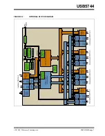
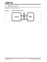
USB5744
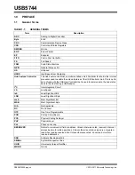
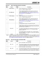
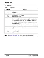
TABLE 3-6:
MISCELLANEOUS PIN DESCRIPTIONS
Num
Pins
Symbol
Buffer
Type
Description
1
RESET_N
IS
The RESET_N pin puts the device into Reset Mode, as the name of
the pin and function then align.
1
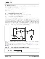
XTALI
ICLK
External 25 MHz crystal input
CLK_IN
ICLK
External reference clock input.
The device may alternatively be driven by a single-ended clock oscil-
lator. When this method is used,
XTALO
should be left unconnected.
1
XTALO
OCLK
External 25 MHz crystal output
1
RBIAS
AI
A 12.0 k
(+/- 1%) resistor is attached from ground to this pin to set
the transceiver’s internal bias settings.
1
ATEST
AI
Analog test pin.
This signal is used for test purposes and must always be connected to
ground.
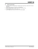
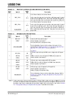
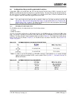
TABLE 3-7:
POWER AND GROUND PIN DESCRIPTIONS
Num
Pins
Symbol
Buffer
Type
Description
4
VDD33
P
+3.3 V power and internal regulator input
Refer to
Section 4.1, "Power Connections"
for power connection infor-
mation.
8
VDD12
P
+1.2 V core power
Refer to
Section 4.1, "Power Connections"
for power connection infor-
mation.
Pad
VSS
P
Common ground.
This exposed pad must be connected to the ground plane with a via
array.


