


Table 4-11. DGI Interface Connections when using I²C
ATtiny3217 Pin
Function
Shared Functionality
PA1
I
2
C SDA
(Data line)
PA2
I
2
C SCL
(Clock line)
Note:
Signal functions in
italic
use alternative pin location. These have to be configured in the PORTMUX register of
the device.
Two GPIO lines are connected to the Embedded Debugger. The EDBG can monitor these lines and timestamp pin
value changes. This makes it possible to accurately timestamp events in the ATtiny3217 application code. For further
information on how to configure and use the GPIO monitoring features, see the
.
Table 4-12. GPIO Lines Connected to the EDBG
ATtiny3217 Pin
Function
Shared Functionality
PB5
GPIO0
PB6
GPIO1
4.4.4
XAM Configuration
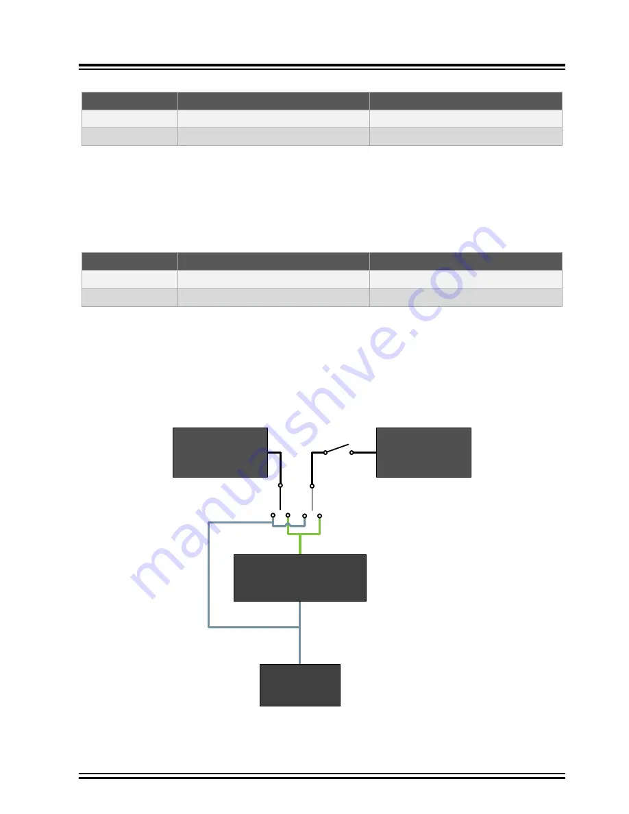
On the ATtiny3217 Xplained Pro, the MCU and the MCU peripherals (e.g., extensions) are powered by their own
regulator, as shown in the figure below. All the other parts of the board, mainly the embedded debugger and the
accompanying Xplained Pro Analog Module (XAM), are powered from a separate regulator. The current to the MCU
and the peripherals can be measured by connecting them to the XAM output through jumper settings.
Figure 4-3. ATtiny3217 Xplained Pro XAM Implementation Block Diagram
Target
Regulator
Current measurement
bypass jumper selection
Target MCU
Target
Peripherals
Xplained Pro MCU power
measurement jumper
Xplained Pro Analog
Module (XAM)
On the ATtiny3217 Xplained Pro the XAM can be used in four configurations:
ATtiny3217 Xplained Pro
Hardware User Guide
©
2020 Microchip Technology Inc.
User Guide
DS50002765B-page 18


