background image

MAX32600 User’s Guide

System Clock, Timers/Counters, Watchdog Timers and Real Time Clock

10.1 System Clock

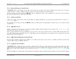
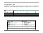
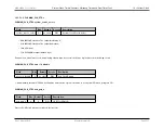
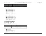
This register field must be left at its default value for proper operation.

CLKMAN_CLK_CONFIG.hfx_gm_adjust

Field

Bits

Default

Access

Description

hfx_gm_adjust

8:4

no effect

R/W

HFX GM Adjust

GM Adjust for Crystal Oscillator Amp

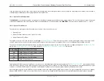
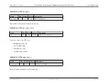
CLKMAN_CLK_CONFIG.hfx_dc_control

Field

Bits

Default

Access

Description

hfx_dc_control

11:9

no effect

R/W

HFX DC Control

Duty Cycle Control for Crystal Oscillator Amp

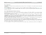
CLKMAN_CLK_CONFIG.pll_enable

Field

Bits

Default

Access

Description

pll_enable

12

no effect

R/W

PLL Enable

Enable Phase Lock Loop clock source generator

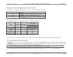
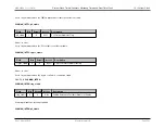
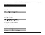
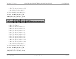
CLKMAN_CLK_CONFIG.pll_reset_n

Field

Bits

Default

Access

Description

pll_reset_n

13

no effect

R/W

PLL ResetN

Rev.1.3 April 2015

Maxim Integrated

Page 513

Summary of Contents for MAX32600

Page 1: ...MAX32600 User s Guide April 2015...

Page 2: ...g 10 2 3 Power Supplies and Modes 10 2 3 1 Digital Supply Voltages 10 2 3 2 Analog Supply Voltage 10 2 3 3 Onboard Core Voltage Regulator 11 2 3 4 Onboard VUSB Voltage Regulator and Automatic Power Sw...

Page 3: ...rogrammable Output Buffers 16 2 6 3 12 Bit Voltage Output DACs 16 2 6 4 8 Bit Voltage Output DACs 17 2 6 5 Uncommitted Op Amps with Comparator Mode 17 2 6 6 Uncommitted SPST Analog Switches 17 2 6 7 T...

Page 4: ...RAM Space 24 3 2 3 Peripheral Space 25 3 2 4 External RAM Space 26 3 2 5 External Device Space 26 3 2 6 System Area Private Peripheral Bus 26 3 2 7 System Area Vendor Defined 26 3 3 Device Memory Inst...

Page 5: ...0 STOP or LP1 STANDBY 32 4 1 2 4 Wakeup Events from LP0 STOP and LP1 STANDBY 33 4 1 3 Low Power Modes LP2 PMU and LP3 RUN 34 4 1 3 1 Low Power Mode 2 LP2 Peripheral Management Unit 35 4 1 3 2 Low Powe...

Page 6: ...terrupt Vector Table 100 4 3 Resets and Reset Sources 102 4 3 1 System Reset 102 4 3 2 Power On Reset 103 4 3 3 RTC POR 103 4 4 Registers IOMAN 103 4 4 1 Module IOMAN Registers 103 4 4 1 1 IOMAN_WUD_R...

Page 7: ...4 1 21 IOMAN_I2CS0_REQ 136 4 4 1 22 IOMAN_I2CS0_ACK 136 4 4 1 23 IOMAN_LCD_COM_REQ 137 4 4 1 24 IOMAN_LCD_COM_ACK 137 4 4 1 25 IOMAN_LCD_SEG_REQ0 137 4 4 1 26 IOMAN_LCD_SEG_REQ1 145 4 4 1 27 IOMAN_LCD...

Page 8: ...GPIO Registers 180 5 5 1 1 GPIO_FREE_Pn 183 5 5 1 2 GPIO_OUT_MODE_Pn 184 5 5 1 3 GPIO_OUT_VAL_Pn 185 5 5 1 4 GPIO_FUNC_SEL_Pn 185 5 5 1 5 GPIO_IN_MODE_Pn 189 5 5 1 6 GPIO_IN_VAL_Pn 190 5 5 1 7 GPIO_I...

Page 9: ...n_CFG 211 6 4 1 3 PMUn_LOOP 214 6 4 1 4 PMUn_OP 214 6 4 1 5 PMUn_DSC1 215 6 4 1 6 PMUn_DSC2 215 6 4 1 7 PMUn_DSC3 215 6 4 1 8 PMUn_DSC4 215 7 Communication Peripherals 216 7 1 I C 216 7 1 1 I C Overvi...

Page 10: ...2 1 Compact Layout 7mm x 7mm Configuration 258 7 2 2 2 Standard Layout 12mm x 12mm Configuration 260 7 2 3 Clock Selection and Configuration 262 7 2 3 1 Clock Gating 263 7 2 4 Configuration Modes Ove...

Page 11: ...Send 288 7 3 8 2 Ready to Send 289 7 3 9 Registers UART 289 7 3 9 1 Module UART Registers 289 7 4 USB Device Interface 300 7 4 1 Overview 300 7 4 2 Operation 301 7 4 2 1 USB Reset Definitions 301 7 4...

Page 12: ...figuration 407 8 3 4 2 Reference Voltage Configuration 409 8 3 4 3 Input Modes 409 8 3 4 4 Input Multiplexer 410 8 3 4 5 Scan Modes 413 8 3 4 6 Interrupts 414 8 3 4 7 Programmable Gain Amplifier 415 8...

Page 13: ...guration 473 8 5 2 2 Multiple LED Configuration 474 8 5 2 3 H bridge LED Configuration 475 8 5 2 4 Independent Loop H bridge LED Configuration 476 8 5 2 5 Integrated Feedback Loops LED Configuration 4...

Page 14: ...ulse Train Outputs 490 9 5 Pulse Train Engine Modes 490 9 5 1 Pulse Train Mode 490 9 5 2 Square Wave Mode 492 9 6 Synchronization 492 9 7 Registers PT 492 9 7 1 Module PT Registers 492 9 7 1 1 PTG_CTR...

Page 15: ...Oscillator 508 10 1 4 ADC Clock Source Configuration 509 10 1 5 Registers CLKMAN 510 10 1 5 1 Module CLKMAN Registers 510 10 2 Watchdog Timers 554 10 2 1 Watchdog Timers Overview 555 10 2 2 Clock Sou...

Page 16: ...1 One Shot Mode 588 10 4 2 2 Continuous Mode 589 10 4 2 3 Counter Mode 590 10 4 2 4 PWM Mode 591 10 4 2 5 Capture Mode 593 10 4 2 6 Compare Mode 593 10 4 2 7 Gated Mode 594 10 4 2 8 Capture Compare M...

Page 17: ...3 1 5 TPU_TSR_CTRL1 629 11 3 1 6 TPU_TSR_SKS0 630 11 3 1 7 TPU_TSR_SKS1 630 11 3 1 8 TPU_TSR_SKS2 630 11 3 1 9 TPU_TSR_SKS3 630 12 CRC16 and CRC32 Hardware Accelerator 631 12 1 Overview 631 12 2 CRC...

Page 18: ...t 638 13 3 5 LCD Port Configuration 640 13 3 6 LCD Memory Configuration 641 13 4 Registers LCD 642 13 4 1 Module LCD Registers 642 13 4 1 1 LCD_LCFG 642 13 4 1 2 LCD_LCRA 644 13 4 1 3 LCD_LPCF 646 13...

Page 19: ...14 1 1 13 FLC_INTEN1 663 14 1 1 14 FLC_DISABLE_XR0 663 14 1 1 15 FLC_DISABLE_XR1 664 14 1 1 16 FLC_DISABLE_XR2 664 14 1 1 17 FLC_DISABLE_XR3 665 14 1 1 18 FLC_DISABLE_WE0 665 14 1 1 19 FLC_DISABLE_WE...

Page 20: ...Inc All rights reserved Information in this publication concerning the devices applications or technology described is intended to suggest possible uses and may be superseded MAXIM INTEGRATED PRODUCTS...

Page 21: ...PMUn_LOOP Corrected descriptions for counter_0 and counter_1 fields 8 2 1 Graphic and label corrections to Figures 8 1 8 2 8 3 and 8 4 8 2 2 1 4 AFE_CTRL2 Corrected field and value descriptions for da...

Page 22: ...ode on the MAX32600 runs from an onboard program flash memory 64 KB to 256 KB with 16 KB to 32 KB SRAM available for general application use A 2 KB instruction cache improves execution throughput and...

Page 23: ...MAX32600 User s Guide Introduction 2 1 Overview Figure 2 1 Block Diagram Rev 1 3 April 2015 Maxim Integrated Page 5...

Page 24: ...saving sleep mode s 2 2 1 Core Parameters When the Cortex M3 core is instantiated in a design values must be selected for configurable parameters in the core For the MAX32600 design core parameters ha...

Page 25: ...NT 1 JTAG Debug Access Port is included on this design CLKGATE_PRESENT 1 Architectural gates are included to minimize dynamic power dissipation OBSERVATION 0 Additional features to observe processor i...

Page 26: ...MAX32600 User s Guide Introduction 2 2 Core and Architecture 2 2 2 Generic Memory Map Figure 2 2 Memory Map Rev 1 3 April 2015 Maxim Integrated Page 8...

Page 27: ...eral bus is a 32 bit bus based on the APB Advanced Peripheral Bus standard It is intended for adding components to the private peripheral bus area which are not intended for general application use si...

Page 28: ...ebug engine pauses the CPU it is important to note that other peripherals and functions on the MAX32600 are not paused and continue to operate normally 2 3 Power Supplies and Modes 2 3 1 Digital Suppl...

Page 29: ...tical components and memories which can remain powered even when the rest of the device is shut down in the lowest possible power savings modes The VRTC supply ensures that the Real Time Clock can con...

Page 30: ...in the datasheet is connected to the part on the 32KIN pin 2 4 3 48MHz USB Clock PLL The phase locked loop PLL clock generation circuit is used to generate a 48MHz clock which is required for proper...

Page 31: ...so provides the ability to directly program a flash location by writing a 32 bit value to the proper memory location using the AHB bus as opposed to setting up the operation directly using the appropr...

Page 32: ...nce the ARM core handles the remapping from the bit banding alias area to a read modify write sequence or single read mask shift for a bit read function of the standard memory area The data SRAM can b...

Page 33: ...least the last stage where trim operations are performed has been completed a lock option setting will be set in the information block to prevent future modifications to the trim and option settings e...

Page 34: ...nt end PGA allows programmable gain settings of 1X 2X 4X and 8X before the input sample is converted The ADC reference voltage is selectable between VAVDD and the dedicated ADC reference level The ADC...

Page 35: ...mps under software control 2 6 6 Uncommitted SPST Analog Switches The device contains four uncommitted SPST analog switches which can be opened and closed under software or pulse train control All SPS...

Page 36: ...t timer counter module also has the option to be split into two separate 16 bit timers dual 16 bit timer mode for a possible total eight timers in the system Each 16 bit timer in this pair has the fol...

Page 37: ...e slave system Depending on the other peripherals and GPIO pins that are in use by the application up to two separate SPI ports are available for general use with a third SPI instance reserved for Blu...

Page 38: ...of one or more segments each of which is activated by selecting the appropriate segment and common signal The microcontroller can multiplex combinations of up to 40 segment outputs SEG0 to SEG39 and...

Page 39: ...processor upon an operation completion and selects whether or not the key expansion generation of first last round key is performed before the encryption or decryption operation begins For multiple bl...

Page 40: ...o be another component of the TPU It allows firmware to perform 512 bit large number modular arithmetic operations which can be used in turn to implement cryptographic algorithms such as RSA The RSA s...

Page 41: ...s most typically accessed in 32 bit 4 byte units It may also be accessed depending on the implementation in 8 bit 1 byte or 16 bit 2 byte widths The total range of the memory space is 32 bits in width...

Page 42: ...on the MAX32600 also contains the mapping for the flash information block from 0x0004_0000 to 0x0004_07FF However this mapping is generally only present during production test it is disabled once the...

Page 43: ...mum On the MAX32600 this includes such functions as the ADC DAC TPU MAA AES etc UART interfaces I C USB etc As with the SRAM region there is a dedicated 1MB area at the bottom of this memory region fr...

Page 44: ...g restricted to the core application code is only allowed to access this area when running in the privileged execution mode as opposed to the standard user thread execution mode This helps ensure that...

Page 45: ...a storage the ARM system stack USB data transfers endpoints and code execution if desired 3 3 5 AES Key and Working Space Memory The AES key memory and working space for AES operations including input...

Page 46: ...e code space This bus master has access to the main flash program memory the information block when it is not locked and the main system SRAM 3 4 3 Core AHB Interface System This AHB master is used by...

Page 47: ...s that dictate the configuration of features during run modes The MAX32600 supports four power modes LP0 STOP LP1 STANDBY LP2 PMU and LP3 RUN The Power State Diagram shows a state diagram of these pow...

Page 48: ...Note Power mode transition restrictions dictate measurement sequences Further transitioning information is found in the power mode sections below The following is a typical measurement sequence LP0 L...

Page 49: ...g support circuitry are available in this mode and to achieve the lowest possible power in LP1 STANDBY it is recommended to turn off all unused analog circuitry This includes the core 1 8V LDO because...

Page 50: ...WRMAN_WUD_CTRL pad_select Enable Active High WUD on P0 0 by setting PWRMAN_WUD_CTRL pad_mode Activate WUD by setting bit 0 of PWRMAN_WUD_PULSE0 Assert GPIO Freeze by setting PWRSEQ_REG1 pwr_gpio_freez...

Page 51: ...turning off the system clock 4 1 2 4 Wakeup Events from LP0 STOP and LP1 STANDBY The following events can wake up the MAX32600 from the Low Power states RTC timer interrupt Timer has 244us resolution...

Page 52: ...gpio_freeze to 0 Clear all flags in PWRSEQ_FLAGS register LP1 Wakeup Read PWRSEQ_FLAGS register to determine the source of the wakeup event If the wakeup event was a GPIO event it is recommended that...

Page 53: ...ional channel draws approximately 100uA of current 4 1 3 2 Low Power Mode 3 LP3 RUN LP3 RUN mode is under full firmware control using the ARM core During this state the ARM Cortex M3 and the digital c...

Page 54: ...MAX32600 User s Guide System Configuration and Management 4 1 Power Ecosystem and Operating Modes Figure 4 2 Power and Clock Gating Options Rev 1 3 April 2015 Maxim Integrated Page 36...

Page 55: ...r Sequencer Power Manager Trickle Charger 1 8V LDO 3 3V USB LDO and Real Time Clock RTC The configuration registers for the Power Manager are within the battery backed VRTC domain The registers are co...

Page 56: ...LP2 PMU or LP3 RUN During LP0 STOP and LP1 STANDBY wakeup interrupts are continuously monitored while consuming very little power Once an interrupt event occurs the Power Sequencer automatically enab...

Page 57: ...STANDBY 4 1 7 4 First Boot Power Up When initial power is applied the PWRSEQ_FLAGS pwr_first_boot flag will be set to indicate the MAX32600 is powering up from a first boot condition The pwr_ first_bo...

Page 58: ...PWRSEQ_FLAGS pwr_brownout_det Setting 10uS 00b 50uS 01b 250uS 10b 750uS 11b Default Note The brownout detect flag PWRSEQ_FLAGS pwr_brownout_det is disabled by default and does not need to be cleared b...

Page 59: ...to USB as its source The 1 8V regulator supports a 50mA maximum capacity 40mA maximum external capacity over an input range of 2 2V to 3 6V and a 30mA maximum capacity 20mA maximum external capacity...

Page 60: ...ected to VSS through a 4 7uF capacitor VDDB Output of USB 5V 3 3V LDO This pin must be connected to VSS through a 4 7uF capacitor VRTC Backup rail or Last Man Standing rail Connect to super capacitor...

Page 61: ...VREFDAC buffers Ground if not used VSS Digital Ground Tie all grounds together on circuit board VSSUB Substrate Ground VSSREF Reference Ground VSSADC ADC Ground VSSDAC DAC Ground Note All grounds are...

Page 62: ...ister 1 0x40090848 PWRMAN_PERIPHERAL_RESET 1 Peripheral Reset Control Register 4 1 12 1 1 PWRMAN_PWR_RST_CTRL PWRMAN_PWR_RST_CTRL flash_active Field Bits Default Access Description flash_active 0 1 R...

Page 63: ...y pins in the lowest power state 1 All I O pins are powered on normally PWRMAN_PWR_RST_CTRL usb_powered Field Bits Default Access Description usb_powered 4 0 R W USB Powered 1 Powers on the USB block...

Page 64: ...l PWRMAN_PWR_RST_CTRL wud_clear Field Bits Default Access Description wud_clear 12 0 R W I O WUD Clear When I O Active bit 3 of PWRMAN_RST_CNTL is deasserted setting this bit will clear the WUD latch...

Page 65: ..._PWR_RST_CTRL arm_lockup Field Bits Default Access Description arm_lockup 20 special R O Reset Caused By ARM Lockup PWRMAN_PWR_RST_CTRL srstn_assertion Field Bits Default Access Description srstn_asse...

Page 66: ...nt monitor detects the monitored condition PWRMAN_INTFL v3_3_warning Field Bits Default Access Description v3_3_warning 1 0 W1C 3 3V Warning Monitor Int Flag Write 1 to clear Set to 1 by hardware when...

Page 67: ...Warning Monitor Int Flag Write 1 to clear Set to 1 by hardware when the associated SVM event monitor detects the monitored condition 4 1 12 1 3 PWRMAN_INTEN PWRMAN_INTEN v1_8_warning Field Bits Defau...

Page 68: ...reset 3 0 R W 3 3V Reset Monitor Int Enable 0 Int disabled 1 Interrupt enabled for the associated SVM monitor event PWRMAN_INTEN vdda_warning Field Bits Default Access Description vdda_warning 4 0 R W...

Page 69: ...Default Access Description rtc_warning 2 n a R O RTC Warning Monitor Event Input Current state of the associated SVM event input PWRMAN_SVM_EVENTS v3_3_reset Field Bits Default Access Description v3_3...

Page 70: ...sponds to P0 0 P0 7 8 15 corresponds to P1 0 P1 7 and so on PWRMAN_WUD_CTRL pad_mode Field Bits Default Access Description pad_mode 9 8 00b R W Wake Up Pad Signal Mode Defines WUD signal to be sent to...

Page 71: ...in WUD_CTRL 0 Clr WUD Weak 1 Set WUD Act Hi 2 Set Weak Hi 3 No pad state change 4 1 12 1 7 PWRMAN_WUD_PULSE1 Default Access Description n a W O WUD Pulse To Mode Bit 1 Writing to this register issues...

Page 72: ...ect Status for P0 6 gpio7 7 0 R O Wake Up Detect Status for P0 7 Displays wakeup detection status of the 8 listed GPIO pads bit 0 Px 0 bit 1 Px 1 bit 2 Px 2 bit 3 Px 3 bit 4 Px 4 bit 5 Px 5 bit 6 Px 6...

Page 73: ...it 1 Px 1 bit 2 Px 2 bit 3 Px 3 bit 4 Px 4 bit 5 Px 5 bit 6 Px 6 bit 7 Px 7 where a 1 bit represents a wakeup condition detected Bits for any I O pads that are not in Wakeup Detect Mode will always re...

Page 74: ...on detected Bits for any I O pads that are not in Wakeup Detect Mode will always read 0 PWRMAN_WUD_SEEN0 gpio24 gpio25 gpio26 gpio27 gpio28 gpio29 gpio30 gpio31 Field Bits Default Access Description g...

Page 75: ...EEN1 PWRMAN_WUD_SEEN1 gpio32 gpio33 gpio34 gpio35 gpio36 gpio37 gpio38 gpio39 Field Bits Default Access Description gpio32 0 0 R O Wake Up Detect Status for P4 0 gpio33 1 0 R O Wake Up Detect Status f...

Page 76: ...6 gpio47 Field Bits Default Access Description gpio40 8 0 R O Wake Up Detect Status for P5 0 gpio41 9 0 R O Wake Up Detect Status for P5 1 gpio42 10 0 R O Wake Up Detect Status for P5 2 gpio43 11 0 R...

Page 77: ...Description gpio48 16 0 R O Wake Up Detect Status for P6 0 gpio49 17 0 R O Wake Up Detect Status for P6 1 gpio50 18 0 R O Wake Up Detect Status for P6 2 gpio51 19 0 R O Wake Up Detect Status for P6 3...

Page 78: ...r P7 1 gpio58 26 0 R O Wake Up Detect Status for P7 2 gpio59 27 0 R O Wake Up Detect Status for P7 3 gpio60 28 0 R O Wake Up Detect Status for P7 4 gpio61 29 0 R O Wake Up Detect Status for P7 5 gpio6...

Page 79: ...ld Bits Default Access Description base_part_number 15 0 n a R O Base Part Number Always returns 3260h base part number PWRMAN_BASE_PART_NUM package_select Field Bits Default Access Description packag...

Page 80: ...Bits Default Access Description mask_id 30 0 n a R O Mask ID 58 28 Mask identification information high 31 bits PWRMAN_MASK_ID1 mask_id_enable Field Bits Default Access Description mask_id_enable 31 0...

Page 81: ...ed to run normally 1 Peripheral is held in a reset state PWRMAN_PERIPHERAL_RESET timer0 Field Bits Default Access Description timer0 2 0 R W Reset Timer0 0 Peripheral is released to run normally 1 Per...

Page 82: ...in a reset state PWRMAN_PERIPHERAL_RESET timer3 Field Bits Default Access Description timer3 5 0 R W Reset Timer3 0 Peripheral is released to run normally 1 Peripheral is held in a reset state PWRMAN_...

Page 83: ...c Field Bits Default Access Description adc 8 0 R W Reset ADC 0 Peripheral is released to run normally 1 Peripheral is held in a reset state PWRMAN_PERIPHERAL_RESET dac0 Field Bits Default Access Desc...

Page 84: ...0 0 Peripheral is released to run normally 1 Peripheral is held in a reset state PWRMAN_PERIPHERAL_RESET dac3 Field Bits Default Access Description dac3 12 0 R W Reset 8 Bit DAC 1 0 Peripheral is rele...

Page 85: ...et state PWRMAN_PERIPHERAL_RESET gpio Field Bits Default Access Description gpio 15 0 R W Reset GPIO Module 0 Peripheral is released to run normally 1 Peripheral is held in a reset state PWRMAN_PERIPH...

Page 86: ...spi1 Field Bits Default Access Description spi1 18 0 R W Reset SPI 1 0 Peripheral is released to run normally 1 Peripheral is held in a reset state PWRMAN_PERIPHERAL_RESET spi2 Field Bits Default Acce...

Page 87: ...1 0 Peripheral is released to run normally 1 Peripheral is held in a reset state PWRMAN_PERIPHERAL_RESET i2cs Field Bits Default Access Description i2cs 22 0 R W Reset I2C Slave 0 Peripheral is relea...

Page 88: ...heral is held in a reset state 4 1 13 Registers PWRSEQ 4 1 13 1 Module PWRSEQ Registers Address Register 32b Word Len Description 0x40090A30 PWRSEQ_REG0 1 Power Sequencer Control Register 0 0x40090A34...

Page 89: ...Access Description pwr_lp1 0 0 PwrSeq RSTN see note R W Shutdown Power Mode Select 0 Shutdown to LP0 default 1 Shutdown to LP1 Note This field is reset by any of the following conditions events PwrSe...

Page 90: ...wrSeq RSTN R W Enable Main 1 8V LDO Operation in Run Mode 3V to 1 8V LDO enable during run default 1 PWRSEQ_REG0 pwr_ldoen_slp Field Bits Default Access Description pwr_ldoen_slp 4 0 PwrSeq RSTN R W E...

Page 91: ...Description pwr_roen_run 7 1 R W Enable System Relaxation Oscillator in Run Mode Relaxation osc enable during run default 1 PWRSEQ_REG0 pwr_roen_slp Field Bits Default Access Description pwr_roen_slp...

Page 92: ...on pwr_rtcen_run 11 0 RTC POR R W Enable Real Time Clock operation in Run Mode Real Time Clock enable during run default 0 PWRSEQ_REG0 pwr_rtcen_slp Field Bits Default Access Description pwr_rtcen_slp...

Page 93: ...efault Access Description pwr_svm1en_run 15 1 PwrSeq RSTN R W Enable VREG18 SVM operation in Run Mode VREG18 SVM enable during run mode default 1 PWRSEQ_REG0 pwr_svm1en_slp Field Bits Default Access D...

Page 94: ...escription pwr_svmvdda3en 19 0 PwrSeq RSTN R W Enable VDDA3 SVM operation in Run Mode only VDDA3 SVM enable can only be enabled during RUN mode default 0 4 1 13 1 2 PWRSEQ_REG1 PWRSEQ_REG1 pwr_trikl_c...

Page 95: ...n VDDA3 Supply Rail 0 VDDA3 supply rail is powered on default 1 VDDA3 supply rail is powered down PWRSEQ_REG1 pwr_temp_sensor_pd Field Bits Default Access Description pwr_temp_sensor_pd 9 1 PwrSeq RST...

Page 96: ...l overrides are enabled for VDDIO_SW1 and VDDIO_SW2 PWRSEQ_REG1 pwr_man_vddio_sw2 Field Bits Default Access Description pwr_man_vddio_sw2 12 0 PwrSeq RSTN R W Manual Override for VDDIO_ SW2 This setti...

Page 97: ...4 0 PwrSeq RSTN R W Freeze GPIO WUD and Keeper Latches 0 GPIO WUD and keeper latches operate normally default 1 GPIO WUD and keeper latches are frozen 4 1 13 1 3 PWRSEQ_REG2 PWRSEQ_REG2 pwr_rst3 Field...

Page 98: ...cription pwr_w1_low 19 15 4 PwrSeq RSTN R W pwr_w1_low_o 4 0 VREG18 Warning LOW decode approx 25mV step size over applicable range PWRSEQ_REG2 pwr_wrtc Field Bits Default Access Description pwr_wrtc 2...

Page 99: ...ble timeout setting in RO clocks 000b Bypass 001b 64 clocks 010b 128 clocks 011b 256 clocks 100b 512 clocks 101b 1024 clocks default setting 110b 2048 clocks 111b 262144 clocks PWRSEQ_REG3 pwr_rosel_q...

Page 100: ...quencer asynchronous reset System Reboot event Whenever pwr_prv_pwr_fail_r 1 Whenever pwr_prv_boot_fail_r 1 PWRSEQ_REG3 pwr_svmsel Field Bits Default Access Description pwr_svmsel 7 5 000b PwrSeq RSTN...

Page 101: ...clocks 00b Bypass 01b 2 clocks 10b 4 clocks 11b 8 clocks default PWRSEQ_REG3 pwr_pwrfltrrosel Field Bits Default Access Description pwr_pwrfltrrosel 12 10 011b PwrSeq RSTN R W pwr_pwrfltrrosel_o 2 0 W...

Page 102: ...o_clk_mux Field Bits Default Access Description pwr_ro_clk_mux 15 0 PwrSeq RSTN R W pwr_ro_clk_mux_o Relaxation Clock mux 0 Relaxation Oscillator default 1 External Clock PWRSEQ_REG3 pwr_quick_cnt Fie...

Page 103: ...ription pwr_tm_ps_2_gpio 0 0 PwrSeq RSTN R W pwr_tm_ps_2_gpio_w Enable power sequencer signals to GPIO pads Test Mode PWRSEQ_REG4 pwr_tm_fast_timers Field Bits Default Access Description pwr_tm_fast_t...

Page 104: ...R W pwr_usbToVddFast_w Switch to VDD rail as soon as VDDBOK is deasserted PWRSEQ_REG4 pwr_usb_ldo_off Field Bits Default Access Description pwr_usb_ldo_off 5 0 PwrSeq RSTN R W pwr_usbLdoOff_w Turn of...

Page 105: ...eg1p8 9 6 0000b PwrSeq RSTN R W pwr_trim_reg1p8_w 3 0 3 volt to 1 8 volt LDO trim PWRSEQ_REG5 pwr_trim_reg3p3 Field Bits Default Access Description pwr_trim_reg3p3 14 10 00000b PwrSeq RSTN R W pwr_tri...

Page 106: ...escription pwr_trim_usb_pm_res 6 3 0000b PwrSeq RSTN R W pwr_trim_usb_pm_ res_o 3 0 USB Data Plus slew rate trim PWRSEQ_REG6 pwr_trim_usb_dm_res Field Bits Default Access Description pwr_trim_usb_dm_r...

Page 107: ...lt Access Description pwr_prv_pwr_fail 2 s W1C pwr_prv_pwr_fail_r Write 1 to clear power fail detect latch Power Fail event detected PWRSEQ_FLAGS pwr_prv_boot_fail Field Bits Default Access Descriptio...

Page 108: ...1 to clear GPIO wakeup event latch GPIO wakeup event detected PWRSEQ_FLAGS pwr_vdd3_rst Field Bits Default Access Description pwr_vdd3_rst 6 s W1C pwr_vdd3_rst_bad_r Write 1 to clear VDD3 reset compa...

Page 109: ...tion pwr_vdd1_low_rst 9 s W1C pwr_vdd1_low_rst_bad_r Write 1 to clear VREG18 reset LOW compare latch VREG18 reset LOW comparator tripped PWRSEQ_FLAGS pwr_vdd1_warn Field Bits Default Access Descriptio...

Page 110: ...OR3_lite have been tripped PWRSEQ_FLAGS rtc_cmpr0 Field Bits Default Access Description rtc_cmpr0 13 s W1C rtc_cmpr0_flag Write 1 to clear causes 4kHz transaction in RTC PWRSEQ_FLAGS rtc_cmpr1 Field B...

Page 111: ...transaction in RTC PWRSEQ_FLAGS pwr_brownout_det Field Bits Default Access Description pwr_brownout_det 17 s W1C pwr_brownout_detected Write 1 to clear PWRSEQ_FLAGS pwr_usb_plug_wakeup Field Bits Def...

Page 112: ...ield Bits Default Access Description pwr_vdd195_rst 21 s W1C pwr_vdd195_rst Write 1 to clear 4 1 13 1 9 PWRSEQ_MSK_FLAGS PWRSEQ_MSK_FLAGS pwr_sys_reboot Field Bits Default Access Description pwr_sys_r...

Page 113: ...ous boot fail detect 0 Event can be detected 1 Event is masked PWRSEQ_MSK_FLAGS pwr_comp_wakeup Field Bits Default Access Description pwr_comp_wakeup 4 0 R W Mask for analog comparator wakeup de tect...

Page 114: ...cted 1 Event is masked PWRSEQ_MSK_FLAGS pwr_vdd3_warn Field Bits Default Access Description pwr_vdd3_warn 7 0 R W Mask for VDD3 voltage warning event detect 0 Event can be detected 1 Event is masked P...

Page 115: ...ts Default Access Description pwr_vdd1_warn 10 0 R W Mask for VREG18 warning level event detect 0 Event can be detected 1 Event is masked PWRSEQ_MSK_FLAGS pwr_vrtc_warn Field Bits Default Access Descr...

Page 116: ...C compare 0 event 0 Event can be detected 1 Event is masked PWRSEQ_MSK_FLAGS rtc_cmpr1 Field Bits Default Access Description rtc_cmpr1 14 0 R W Mask for RTC compare 1 event 0 Event can be detected 1 E...

Page 117: ...Event is masked PWRSEQ_MSK_FLAGS pwr_brownout_det Field Bits Default Access Description pwr_brownout_det 17 1 R W Mask for power brownout detect Note Masked by default 0 Event can be detected 1 Event...

Page 118: ...0 Event can be detected 1 Event is masked PWRSEQ_MSK_FLAGS pwr_vdd22_rst Field Bits Default Access Description pwr_vdd22_rst 20 0 R W Mask for VDD22 reset event 0 Event can be detected 1 Event is mask...

Page 119: ...PI1 11 0x6c SPI2 12 0x70 Timer 0 Lower timer in 16 bit mode or 32 bit timer 13 0x74 Timer 1 Lower timer in 16 bit mode or 32 bit timer 14 0x78 Timer 2 Lower timer in 16 bit mode or 32 bit timer 15 0x7...

Page 120: ...timer in 16 bit mode 43 0xec Timer 1 Upper timer in 16 bit mode 44 0xf0 Timer 2 Upper timer in 16 bit mode 45 0xf4 Timer 3 Upper timer in 16 bit mode 46 0xf8 I2 C Master 1 4 3 Resets and Reset Sources...

Page 121: ...still retained as long as the backup supply VRTC is still available A failure of the VRTC supply in combination with a standard POR causes a full reset of the RTC core and all registers and internal...

Page 122: ...4 IOMAN_I2CS0_ACK 1 I2C Slave 0 I O Acknowledge 0x40090C58 IOMAN_LCD_COM_REQ 1 LCD COM Driver I O Request 0x40090C5C IOMAN_LCD_COM_ACK 1 LCD COM Driver I O Acknowledge 0x40090C60 IOMAN_LCD_SEG_REQ0 1...

Page 123: ...sociated GPIO pin IOMAN_WUD_REQ0 port1 Field Bits Default Access Description port1 15 8 00000000b R W Wakeup Detect Request Mode P1 7 0 0 No effect 1 Requests enable of wakeup detect mode on the assoc...

Page 124: ...Access Description port4 7 0 00000000b R W Wakeup Detect Request Mode P4 7 0 0 No effect 1 Requests enable of wakeup detect mode on the associated GPIO pin IOMAN_WUD_REQ1 port5 Field Bits Default Acc...

Page 125: ...ct mode on the associated GPIO pin 4 4 1 3 IOMAN_WUD_ACK0 IOMAN_WUD_ACK0 port0 Field Bits Default Access Description port0 7 0 00000000b R O WUD Mode Acknowledge P0 7 0 A 1 value indicates that the as...

Page 126: ...1 value indicates that the associated pin has been enabled for wakeup detection mode 4 4 1 4 IOMAN_WUD_ACK1 IOMAN_WUD_ACK1 port4 Field Bits Default Access Description port4 7 0 00000000b R O WUD Mode...

Page 127: ...port7 31 24 00000000b R O WUD Mode Acknowledge P7 7 0 A 1 value indicates that the associated pin has been enabled for wakeup detection mode 4 4 1 5 IOMAN_ALI_REQ0 IOMAN_ALI_REQ0 port0 Field Bits Defa...

Page 128: ...analog input mode on the associated pin IOMAN_ALI_REQ0 port3 Field Bits Default Access Description port3 31 24 00000000b R W Analog Input Mode Request P3 7 0 0 No effect 1 Requests analog input mode...

Page 129: ...pin IOMAN_ALI_REQ1 port6 Field Bits Default Access Description port6 23 16 00000000b R W Analog Input Mode Request P6 7 0 0 No effect 1 Requests analog input mode on the associated pin IOMAN_ALI_REQ1...

Page 130: ...A 1 value indicates that the associated pin has been enabled for analog input mode IOMAN_ALI_ACK0 port2 Field Bits Default Access Description port2 23 16 00000000b R O Analog In Mode Acknowledge P2 7...

Page 131: ...1 value indicates that the associated pin has been enabled for analog input mode IOMAN_ALI_ACK1 port6 Field Bits Default Access Description port6 23 16 00000000b R O Analog In Mode Acknowledge P6 7 0...

Page 132: ...g C if supported 11b Select pin mapping D if supported IOMAN_SPI0_REQ core_io Field Bits Default Access Description core_io 4 0 R W SPI0 Core I O Request 1 Requests SPI mode for SCLK SDIO 0 and SDIO 1...

Page 133: ...S 2 IOMAN_SPI0_REQ ss3_io Field Bits Default Access Description ss3_io 11 0 R W SPI0 SS 3 I O Request 1 Requests SPI mode for SS 3 IOMAN_SPI0_REQ ss4_io Field Bits Default Access Description ss4_io 12...

Page 134: ...cription quad_io 20 0 R W SPI0 Quad I O Request 1 Requests SPI mode for SDIO 2 and SDIO 3 IOMAN_SPI0_REQ fast_mode Field Bits Default Access Description fast_mode 24 0 R W SPI0 Fast Mode 1 Enables fas...

Page 135: ..._io Field Bits Default Access Description ss0_io 8 0 R O SPI0 SS 0 I O Acknowledge 1 Acknowledges SPI0 mode selected for SS 0 IOMAN_SPI0_ACK ss1_io Field Bits Default Access Description ss1_io 9 0 R O...

Page 136: ...Bits Default Access Description ss4_io 12 0 R O SPI0 SS 4 I O Acknowledge 1 Acknowledges SPI0 mode selected for SS 4 IOMAN_SPI0_ACK sr0_io Field Bits Default Access Description sr0_io 16 0 R O SPI0 SR...

Page 137: ...tion fast_mode 24 0 R O SPI0 Fast Mode Acknowledge 4 4 1 11 IOMAN_SPI1_REQ IOMAN_SPI1_REQ mapping Field Bits Default Access Description mapping 1 0 00b R W SPI1 I O Mapping Select 00b Select pin mappi...

Page 138: ...ode for SS 0 IOMAN_SPI1_REQ ss1_io Field Bits Default Access Description ss1_io 9 0 R W SPI1 SS 1 I O Request 1 Requests SPI mode for SS 1 IOMAN_SPI1_REQ ss2_io Field Bits Default Access Description s...

Page 139: ..._io Field Bits Default Access Description sr0_io 16 0 R W SPI1 SR 0 I O Request 1 Requests SPI mode for SR 0 IOMAN_SPI1_REQ sr1_io Field Bits Default Access Description sr1_io 17 0 R W SPI1 SR 1 I O R...

Page 140: ...ult Access Description mapping 1 0 00b R O SPI1 I O Mapping Acknowledge Mirror of I O mapping select bits from REQ bits 1 0 IOMAN_SPI1_ACK core_io Field Bits Default Access Description core_io 4 0 R O...

Page 141: ...its Default Access Description ss2_io 10 0 R O SPI1 SS 2 I O Acknowledge 1 Acknowledges SPI1 mode selected for SS 2 IOMAN_SPI1_ACK ss3_io Field Bits Default Access Description ss3_io 11 0 R O SPI1 SS...

Page 142: ...ult Access Description sr1_io 17 0 R O SPI1 SR 1 I O Acknowledge 1 Acknowledges SPI1 mode selected for SR 1 IOMAN_SPI1_ACK quad_io Field Bits Default Access Description quad_io 20 0 R O SPI1 Quad I O...

Page 143: ...g C if supported 11b Select pin mapping D if supported IOMAN_SPI2_REQ core_io Field Bits Default Access Description core_io 4 0 R W SPI2 Core I O Request 1 Requests SPI mode for SCLK SDIO 0 and SDIO 1...

Page 144: ...S 2 IOMAN_SPI2_REQ ss3_io Field Bits Default Access Description ss3_io 11 0 R W SPI2 SS 3 I O Request 1 Requests SPI mode for SS 3 IOMAN_SPI2_REQ ss4_io Field Bits Default Access Description ss4_io 12...

Page 145: ...cription quad_io 20 0 R W SPI2 Quad I O Request 1 Requests SPI mode for SDIO 2 and SDIO 3 IOMAN_SPI2_REQ fast_mode Field Bits Default Access Description fast_mode 24 0 R W SPI2 Fast Mode 1 Enables fas...

Page 146: ..._io Field Bits Default Access Description ss0_io 8 0 R O SPI2 SS 0 I O Acknowledge 1 Acknowledges SPI2 mode selected for SS 0 IOMAN_SPI2_ACK ss1_io Field Bits Default Access Description ss1_io 9 0 R O...

Page 147: ...Bits Default Access Description ss4_io 12 0 R O SPI2 SS 4 I O Acknowledge 1 Acknowledges SPI2 mode selected for SS 4 IOMAN_SPI2_ACK sr0_io Field Bits Default Access Description sr0_io 16 0 R O SPI2 SR...

Page 148: ...n fast_mode 24 0 R O SPI2 Fast Mode Acknowledge 4 4 1 15 IOMAN_UART0_REQ IOMAN_UART0_REQ mapping Field Bits Default Access Description mapping 1 0 00b R W UART0 I O Mapping Select 00b Select pin mappi...

Page 149: ...EQ rts_io Field Bits Default Access Description rts_io 6 0 R W UART0 RTS I O Request 1 Requests UART0 mode for RTS pin 4 4 1 16 IOMAN_UART0_ACK IOMAN_UART0_ACK mapping Field Bits Default Access Descri...

Page 150: ...N_UART0_ACK rts_io Field Bits Default Access Description rts_io 6 0 R O UART0 RTS I O Acknowledge 1 Acknowledges UART0 mode selected for RTS 4 4 1 17 IOMAN_UART1_REQ IOMAN_UART1_REQ mapping Field Bits...

Page 151: ...fault Access Description cts_io 5 0 R W UART1 CTS I O Request 1 Requests UART1 mode for CTS pin IOMAN_UART1_REQ rts_io Field Bits Default Access Description rts_io 6 0 R W UART1 RTS I O Request 1 Requ...

Page 152: ...Access Description cts_io 5 0 R O UART1 CTS I O Acknowledge 1 Acknowledges UART1 mode selected for CTS IOMAN_UART1_ACK rts_io Field Bits Default Access Description rts_io 6 0 R O UART1 RTS I O Acknow...

Page 153: ...W I2C Master I O Request 1 Requests I2C Master mode for SCL and SDA pins 4 4 1 20 IOMAN_I2CM0_ACK IOMAN_I2CM0_ACK mapping Field Bits Default Access Description mapping 1 0 00b R O I2C Master I O Mappi...

Page 154: ...ping B if supported 10b Select pin mapping C if supported 11b Select pin mapping D if supported IOMAN_I2CS0_REQ core_io Field Bits Default Access Description core_io 4 0 R W I2C Slave I O Request 1 Re...

Page 155: ...Field Bits Default Access Description com_io 0 0 R W LCD COM I O Request 1 Requests LCD COM mode for COM 3 0 all four 4 4 1 24 IOMAN_LCD_COM_ACK IOMAN_LCD_COM_ACK com_io Field Bits Default Access Desc...

Page 156: ...for this GPIO P3 1 IOMAN_LCD_SEG_REQ0 io_req_26 Field Bits Default Access Description io_req_26 2 0 R W LCD SEG I O Request for GPIO 26 1 Requests LCD SEG mode for this GPIO P3 2 IOMAN_LCD_SEG_REQ0 io...

Page 157: ...req_30 Field Bits Default Access Description io_req_30 6 0 R W LCD SEG I O Request for GPIO 30 1 Requests LCD SEG mode for this GPIO P3 6 IOMAN_LCD_SEG_REQ0 io_req_31 Field Bits Default Access Descrip...

Page 158: ...lt Access Description io_req_34 10 0 R W LCD SEG I O Request for GPIO 34 1 Requests LCD SEG mode for this GPIO P4 2 IOMAN_LCD_SEG_REQ0 io_req_35 Field Bits Default Access Description io_req_35 11 0 R...

Page 159: ...ult Access Description io_req_38 14 0 R W LCD SEG I O Request for GPIO 38 1 Requests LCD SEG mode for this GPIO P4 6 IOMAN_LCD_SEG_REQ0 io_req_39 Field Bits Default Access Description io_req_39 15 0 R...

Page 160: ...ult Access Description io_req_42 18 0 R W LCD SEG I O Request for GPIO 42 1 Requests LCD SEG mode for this GPIO P5 2 IOMAN_LCD_SEG_REQ0 io_req_43 Field Bits Default Access Description io_req_43 19 0 R...

Page 161: ...ult Access Description io_req_46 22 0 R W LCD SEG I O Request for GPIO 46 1 Requests LCD SEG mode for this GPIO P5 6 IOMAN_LCD_SEG_REQ0 io_req_47 Field Bits Default Access Description io_req_47 23 0 R...

Page 162: ...ult Access Description io_req_50 26 0 R W LCD SEG I O Request for GPIO 50 1 Requests LCD SEG mode for this GPIO P6 2 IOMAN_LCD_SEG_REQ0 io_req_51 Field Bits Default Access Description io_req_51 27 0 R...

Page 163: ...cription io_req_54 30 0 R W LCD SEG I O Request for GPIO 54 1 Requests LCD SEG mode for this GPIO P6 6 IOMAN_LCD_SEG_REQ0 io_req_55 Field Bits Default Access Description io_req_55 31 0 R W LCD SEG I O...

Page 164: ...ault Access Description io_req_58 2 0 R W LCD SEG I O Request for GPIO 58 1 Requests LCD SEG mode for this GPIO P7 2 IOMAN_LCD_SEG_REQ1 io_req_59 Field Bits Default Access Description io_req_59 3 0 R...

Page 165: ...scription io_req_62 6 0 R W LCD SEG I O Request for GPIO 62 1 Requests LCD SEG mode for this GPIO P7 6 IOMAN_LCD_SEG_REQ1 io_req_63 Field Bits Default Access Description io_req_63 7 0 R W LCD SEG I O...

Page 166: ...fault Access Description io_ack_26 2 0 R O LCD SEG I O Acknowledge for GPIO 26 1 Acknowledges SEG mode selected P3 2 IOMAN_LCD_SEG_ACK0 io_ack_27 Field Bits Default Access Description io_ack_27 3 0 R...

Page 167: ...fault Access Description io_ack_30 6 0 R O LCD SEG I O Acknowledge for GPIO 30 1 Acknowledges SEG mode selected P3 6 IOMAN_LCD_SEG_ACK0 io_ack_31 Field Bits Default Access Description io_ack_31 7 0 R...

Page 168: ...ult Access Description io_ack_34 10 0 R O LCD SEG I O Acknowledge for GPIO 34 1 Acknowledges SEG mode selected P4 2 IOMAN_LCD_SEG_ACK0 io_ack_35 Field Bits Default Access Description io_ack_35 11 0 R...

Page 169: ...ault Access Description io_ack_38 14 0 R O LCD SEG I O Acknowledge for GPIO 38 1 Acknowledges SEG mode selected P4 6 IOMAN_LCD_SEG_ACK0 io_ack_39 Field Bits Default Access Description io_ack_39 15 0 R...

Page 170: ...ault Access Description io_ack_42 18 0 R O LCD SEG I O Acknowledge for GPIO 42 1 Acknowledges SEG mode selected P5 2 IOMAN_LCD_SEG_ACK0 io_ack_43 Field Bits Default Access Description io_ack_43 19 0 R...

Page 171: ...ault Access Description io_ack_46 22 0 R O LCD SEG I O Acknowledge for GPIO 46 1 Acknowledges SEG mode selected P5 6 IOMAN_LCD_SEG_ACK0 io_ack_47 Field Bits Default Access Description io_ack_47 23 0 R...

Page 172: ...ault Access Description io_ack_50 26 0 R O LCD SEG I O Acknowledge for GPIO 50 1 Acknowledges SEG mode selected P6 2 IOMAN_LCD_SEG_ACK0 io_ack_51 Field Bits Default Access Description io_ack_51 27 0 R...

Page 173: ...scription io_ack_54 30 0 R O LCD SEG I O Acknowledge for GPIO 54 1 Acknowledges SEG mode selected P6 6 IOMAN_LCD_SEG_ACK0 io_ack_55 Field Bits Default Access Description io_ack_55 31 0 R O LCD SEG I O...

Page 174: ...fault Access Description io_ack_58 2 0 R O LCD SEG I O Acknowledge for GPIO 58 1 Acknowledges SEG mode selected P7 2 IOMAN_LCD_SEG_ACK1 io_ack_59 Field Bits Default Access Description io_ack_59 3 0 R...

Page 175: ...2 1 Acknowledges SEG mode selected P7 6 IOMAN_LCD_SEG_ACK1 io_ack_63 Field Bits Default Access Description io_ack_63 7 0 R O LCD SEG I O Acknowledge for GPIO 63 1 Acknowledges SEG mode selected P7 7 4...

Page 176: ...I O mode for drain source pair 4 4 1 30 IOMAN_CRNT_ACK IOMAN_CRNT_ACK io_ack_crnt0 Field Bits Default Access Description io_ack_crnt0 0 0 R O Acknowledge for pair CRNT0 1 Acknowledges Current Drive I...

Page 177: ...Field Bits Default Access Description io_ack_crnt4 4 0 R O Acknowledge for pair CRNT4 1 Acknowledges Current Drive I O mode enabled for this pair IOMAN_CRNT_ACK io_ack_crnt5 Field Bits Default Access...

Page 178: ...r CRNT0 io_crnt1 7 4 0000b R W Current Drive Mode Select for pair CRNT1 io_crnt2 11 8 0000b R W Current Drive Mode Select for pair CRNT2 io_crnt3 15 12 0000b R W Current Drive Mode Select for pair CRN...

Page 179: ...OMAN_ALI_CONNECT1 Default Access Description 00000000h R W Analog I O Connection Control Register 1 Selects analog connection input for last 32 GPIO 4 4 1 34 IOMAN_I2CM1_REQ IOMAN_I2CM1_REQ mapping Fi...

Page 180: ...Default Access Description mapping 1 0 00b R O I2C Master I O Mapping Acknowledge Mirror of I O mapping select bits from REQ bits 1 0 IOMAN_I2CM1_ACK core_io Field Bits Default Access Description cor...

Page 181: ...ive mode for GPIO PADX pad 0 High impedance 1 Pullup 2 Drive 0 3 Drive 1 IOMAN_PADX_CONTROL padx_gpio0_input_state Field Bits Default Access Description padx_gpio0_input_state 6 0 R O PADX GPIO0 Input...

Page 182: ...s IOMAN 0 High impedance 1 Pullup 2 Drive 0 3 Drive 1 IOMAN_PADX_CONTROL padx_gpio1_input_state Field Bits Default Access Description padx_gpio1_input_state 10 0 R O PADX GPIO1 Input Value Returns inp...

Page 183: ...n layout is featured on the 12mm x 12mm package and contains all GPIO ports available on the MAX32600 P0 through P7 It also includes LCD functionality Compact Pin Layout The Compact pin layout is feat...

Page 184: ...it timer input or output GPIO functionality is enabled by default for any GPIO pin that does not have any other function selected All GPIO pins can be enabled for external interrupt mode and or wakeup...

Page 185: ...Pin Configurations Packages and Special Function Multiplexing 5 2 Pin Function Mapping Figure 5 1 Compact Port 0 IO Function Muxing Figure 5 2 Compact Port 1 IO Function Muxing Rev 1 3 April 2015 Maxi...

Page 186: ...and Special Function Multiplexing 5 2 Pin Function Mapping Figure 5 3 Compact Port 2 IO Function Muxing 5 2 2 Standard Package GPIO Mapping GPIO port and pin mapping for the Standard Package 12mm x 1...

Page 187: ...in Configurations Packages and Special Function Multiplexing 5 2 Pin Function Mapping Figure 5 4 Standard Port 0 IO Function Muxing Figure 5 5 Standard Port 1 IO Function Muxing Rev 1 3 April 2015 Max...

Page 188: ...in Configurations Packages and Special Function Multiplexing 5 2 Pin Function Mapping Figure 5 6 Standard Port 2 IO Function Muxing Figure 5 7 Standard Port 3 IO Function Muxing Rev 1 3 April 2015 Max...

Page 189: ...in Configurations Packages and Special Function Multiplexing 5 2 Pin Function Mapping Figure 5 8 Standard Port 4 IO Function Muxing Figure 5 9 Standard Port 5 IO Function Muxing Rev 1 3 April 2015 Max...

Page 190: ...n Configurations Packages and Special Function Multiplexing 5 2 Pin Function Mapping Figure 5 10 Standard Port 6 IO Function Muxing Figure 5 11 Standard Port 7 IO Function Muxing Rev 1 3 April 2015 Ma...

Page 191: ...of the pin e g normal drive vs open drain or high impedance Regardless of the selected function for a given pin firmware can always monitor the current logic level of the pin using the appropriate reg...

Page 192: ...errupt vector channels Interrupt Number Vector Description 34 0xc8 External interrupt triggered on one or more pins of GPIO Port 0 35 0xcc External interrupt triggered on one or more pins of GPIO Port...

Page 193: ...for certain events and to generate interrupts to the processor on detection of these events Input monitoring functions as expected regardless of pad ownership The user can enable interrupt generation...

Page 194: ...on Function Description Direction P0 0 P1 0 P2 0 P3 0 P4 0 P5 0 P6 0 P7 0 GPIO Port Pin Px 0 Port Pin Firmware Controlled In Out X X X X X X X X Pulse Train 0 PT0 Pulse Train 0 Output Out X X X X X Pu...

Page 195: ...t Timer 0 TMR0 32 bit Timer Counter 0 Input or Out put In Out X X X X X Px 2 GPIO Pins and Functions Function Support by Port Px 2 x 0 to 7 Peripheral Pin Function Function Description Direction P0 2...

Page 196: ...Out put In Out X X X X X 32 bit Timer 1 TMR1 32 bit Timer Counter 1 Input or Out put In Out X X X X X 32 bit Timer 2 TMR2 32 bit Timer Counter 2 Input or Out put In Out X X X X X Px 4 GPIO Pins and F...

Page 197: ...Pulse Train 2 Output Out X X X X X 32 bit Timer 1 TMR1 32 bit Timer Counter 1 Input or Out put In Out X X X X X 32 bit Timer 2 TMR2 32 bit Timer Counter 2 Input or Out put In Out X X X X X 32 bit Time...

Page 198: ...Function Function Description Direction P0 7 P1 7 P2 7 P3 7 P4 7 P5 7 P6 7 P7 7 GPIO Port Pin Px 7 Port Pin Firmware Controlled In Out X X X X X X X X Pulse Train 7 PT7 Pulse Train 7 Output Out X X X...

Page 199: ...DE_P3 1 Port P3 GPIO Output Drive Mode 0x40000090 GPIO_OUT_MODE_P4 1 Port P4 GPIO Output Drive Mode 0x40000094 GPIO_OUT_MODE_P5 1 Port P5 GPIO Output Drive Mode 0x40000098 GPIO_OUT_MODE_P6 1 Port P6 G...

Page 200: ...1 Port P3 GPIO Input Value 0x40000190 GPIO_IN_VAL_P4 1 Port P4 GPIO Input Value 0x40000194 GPIO_IN_VAL_P5 1 Port P5 GPIO Input Value 0x40000198 GPIO_IN_VAL_P6 1 Port P6 GPIO Input Value 0x4000019C GPI...

Page 201: ...PIO_FREE_Pn pin0 pin1 pin2 pin3 pin4 pin5 pin6 pin7 Field Bits Default Access Description pin0 0 s R O Pn 0 GPIO Mode Acknowledge pin1 1 s R O Pn 1 GPIO Mode Acknowledge pin2 2 s R O Pn 2 GPIO Mode Ac...

Page 202: ...in1 7 4 0000b R W Pn 1 Output Drive Mode pin2 11 8 0000b R W Pn 2 Output Drive Mode pin3 15 12 0000b R W Pn 3 Output Drive Mode pin4 19 16 0000b R W Pn 4 Output Drive Mode pin5 23 20 0000b R W Pn 5 Ou...

Page 203: ...3 1 R W Pn 3 GPIO Output Drive Value pin4 4 1 R W Pn 4 GPIO Output Drive Value pin5 5 1 R W Pn 5 GPIO Output Drive Value pin6 6 1 R W Pn 6 GPIO Output Drive Value pin7 7 1 R W Pn 7 GPIO Output Drive V...

Page 204: ...Pn 1 Output Function Select 0 Firmware control with OUT_VAL 1 Pulse train 1 2 Pulse train 4 3 Pulse train 0 4 32 bit Timer 1 I O 5 32 bit Timer 2 I O 6 32 bit Timer 3 I O 7 32 bit Timer 0 I O GPIO_FUN...

Page 205: ...ess Description pin3 15 12 0000b R W Pn 3 Output Function Select 0 Firmware control with OUT_VAL 1 Pulse train 3 2 Pulse train 5 3 Pulse train 1 4 32 bit Timer 3 I O 5 32 bit Timer 0 I O 6 32 bit Time...

Page 206: ..._FUNC_SEL_Pn pin5 Field Bits Default Access Description pin5 23 20 0000b R W Pn 5 Output Function Select 0 Firmware control with OUT_VAL 1 Pulse train 5 2 Pulse train 6 3 Pulse train 2 4 32 bit Timer...

Page 207: ...t Timer 0 I O 7 32 bit Timer 1 I O GPIO_FUNC_SEL_Pn pin7 Field Bits Default Access Description pin7 31 28 0000b R W Pn 7 Output Function Select 0 Firmware control with OUT_VAL 1 Pulse train 7 2 Pulse...

Page 208: ...oring Mode Determines how corresponding GPIO Input Value bit is calculated also affects input signal for interrupt detection on this pin if enabled 00b Normal input 01b Inverted input 10b Always retur...

Page 209: ...de pin3 14 12 000b R W Pn 3 GPIO Interrupt Detection Mode pin4 18 16 000b R W Pn 4 GPIO Interrupt Detection Mode pin5 22 20 000b R W Pn 5 GPIO Interrupt Detection Mode pin6 26 24 000b R W Pn 6 GPIO In...

Page 210: ...his bit writes to 0 have no effect Set to 1 by hardware when an interrupt has been detected on this pin 5 5 1 9 GPIO_INTEN_Pn GPIO_INTEN_Pn pin0 pin1 pin2 pin3 pin4 pin5 pin6 pin7 Field Bits Default A...

Page 211: ...l operations switching the CPU off and handling the operations using the PMU provides a lower noise environment that is critical for obtaining optimum analog to digital converter ADC and digital to an...

Page 212: ...MAX32600 User s Guide Peripheral Management Unit PMU 6 1 Overview Figure 6 1 PMU Interface Rev 1 3 April 2015 Maxim Integrated Page 194...

Page 213: ...his register also reports status and error information 6 2 1 PMU Channel Setup To begin execution on a PMU channel the user must specify an area of memory which may be RAM or Flash memory to hold the...

Page 214: ...Code MOVE 0x00 The MOVE op code is used to move a user specified block of data from the read address location to the write address location Read and write addresses may be in either the AHB or APB me...

Page 215: ...ementing of the read address This may be useful when reading from FIFO storage elements WR INC Setting this bit to 1 enables auto incrementing of the write address This may be useful when writing to S...

Page 216: ...rminate op code processing after execution This also clears the START bit field in the PMUn_CFG register 6 3 3 PMU Op Code WAIT 0x02 The WAIT op code will suspend the execution of subsequent op codes...

Page 217: ...e interrupts do not require the user to clear or enable the interrupt source they are self clearing and enabled by the appropriate FIFO configuration registers as shown in the table below PMU FIFO Int...

Page 218: ...ifo_af_lvl 20 SPI2 trans_fifo_empty Interrupt is set when FIFO level falls below the user defined threshold in the SPI2_FIFO_CTRL tx_fifo_ae_lvl register field the interrupt self clears when the FIFO...

Page 219: ...AA_CTRL inten to enable MAA_CTRL if_done to clear W0C 32 SPI0 rx_stalled OR tx_ready OR tx_stalled SPI0_INTEN rx_stalled SPI0_INTEN tx_stalled or SPI0_INTEN tx_ready to enable SPI0_INTFL rx_ stalled S...

Page 220: ...in 7 0 to clear W1C 46 Interrupts on Port 6 GPIO GPIO_INT_MODE_P6 pin 7 0 to enable GPIO_INTFL_P6 pin 7 0 to clear W1C 47 Interrupts on Port 7 GPIO GPIO_INT_MODE_P7 pin 7 0 to enable GPIO_INTFL_P7 pin...

Page 221: ...ode is executed by the PMU engine When the specified loop counter reaches zero the next sequential op code will be fetched The zero check is performed after the specified counter is decremented The IN...

Page 222: ...sses are restricted to 32 bit accesses When the bit s set in the data mask match those in the expected data field the execution of this op code will terminate The polling interval is specified in syst...

Page 223: ...l address 6 3 7 PMU Op Code BRANCH 0x06 The BRANCH op code will cause the PMU engine to read the specified address location and fetch the next op code from the specified location when the bit s set in...

Page 224: ...ite address location in burst size blocks in bytes as specified by the user Transfers are only performed when the specified bit s in the interrupt mask 31 0 are set The TRANSFER op code will continue...

Page 225: ...the CPU upon completion of this op code STOP Set to 1 if this op code is to terminate op code processing after execution This also clears the START bit field in the PMUn_CFG register RD SIZE WR SIZE...

Page 226: ...bit writes 10b 10b Perform 32 bit reads and writes XX 11 Reserved 11b XX Reserved RD INC Setting this bit to 0 disables auto incrementing of the read address This may be useful when reading from FIFO...

Page 227: ...ORD 0 OP 0x40070030 PMU1_DSC1 1 Current Descriptor DWORD 1 0x40070034 PMU1_DSC2 1 Current Descriptor DWORD 2 0x40070038 PMU1_DSC3 1 Current Descriptor DWORD 3 0x4007003C PMU1_DSC4 1 Current Descriptor...

Page 228: ...70094 PMU4_DSC2 1 Current Descriptor DWORD 2 0x40070098 PMU4_DSC3 1 Current Descriptor DWORD 3 0x4007009C PMU4_DSC4 1 Current Descriptor DWORD 4 0x400700A0 PMU5_DSCADR 1 Starting Descriptor Address 0x...

Page 229: ...l only PMUn_CFG ll_stopped Field Bits Default Access Description ll_stopped 2 1 R W Linked List Engine Status 0 Not stopped 1 Stopped Set to 1 by hardware when the LL Engine executes a descriptor with...

Page 230: ...on an AHB bus error condition PMUn_CFG to_stat Field Bits Default Access Description to_stat 6 0 W1C AHB Bus Timeout Interrupt Flag Write 1 to clear Set to 1 by hardware when an AHB bus timeout occurs...

Page 231: ...generate the timeout counter 00b Disabled default 01b Clock div 256 10b Clock div 64K 11b Clock div 16M PMUn_CFG interrupt Field Bits Default Access Description interrupt 16 0 W1C Descriptor Interrupt...

Page 232: ...ts Default Access Description burst_size 28 24 00000b R W DMA Maximum Burst Size This field controls the maximum size of the PMU transfer bursts in bytes e g 10h 16 bytes or 4 dwords 6 4 1 3 PMUn_LOOP...

Page 233: ...Current Descriptor DWORD 1 6 4 1 6 PMUn_DSC2 Default Access Description 00000000h R W Current Descriptor DWORD 2 6 4 1 7 PMUn_DSC3 Default Access Description 00000000h R W Current Descriptor DWORD 3 6...

Page 234: ...pin and generate the START and STOP signals This enables the MAX32600 to send and receive data from a slave as required by the user s application In slave mode the device relies on an externally gene...

Page 235: ...for maximum flexibility Speed Categories The I2 C master ports support two operating speed categories Standard mode with a bit rate up to 100Kbps Fast mode with a bit rate up to 400Kbps Note All inte...

Page 236: ...ation Peripherals 7 1 I C Figure 7 1 Compact Package Mapping Options I C Master Configurations Compact I2CM0 Logic Signal Port and Pin SDA A P1 4 B P2 2 D P0 4 SCL A P1 5 B P2 3 D P0 5 Rev 1 3 April 2...

Page 237: ...ons Compact I2CS Logic Signal Port and Pin SDA A P1 4 B P2 2 D P0 4 E P1 6 F P2 6 H P0 6 SCL A P1 5 B P2 3 D P0 5 E P1 7 F P2 7 H P0 7 7 1 3 2 Standard Layout 12mm x 12mm Configuration Available SDA a...

Page 238: ...MAX32600 User s Guide Communication Peripherals 7 1 I C Figure 7 2 Standard Package Mapping Options Rev 1 3 April 2015 Maxim Integrated Page 220...

Page 239: ...tandard I2CM0 Logic Signal Port and Pin SDA A P2 4 B P2 2 C P7 4 D P0 4 SCL A P2 5 B P2 3 C P7 5 D P0 5 I2CM1 Logic Signal Port and Pin SDA A P2 6 B P1 6 C P7 6 D P0 6 SCL A P2 7 B P1 7 C P7 7 D P0 7...

Page 240: ...Results FIFO An unexpected NACK on write data results in system interrupt In this case hardware can be opted to automatically issue a Stop under this condition to free the bus Results FIFO records the...

Page 241: ...100Kbps in standard mode and up to 400Kbits 400Kbps in fast mode Transfer Protocol Each transfer is made of a start bit followed by one or more sequences of eight data bits acknowledge bit s sent by...

Page 242: ...s the SDA line during the acknowledge clock pulse so the receiver can pull the SDA line to the low state it remains stable in the low state during the high period of this clock pulse on the SCL line S...

Page 243: ...equire data from the general call address acknowledges the address and behaves as a slave receiver a device that does not require any of the data supplied within the general call address does not have...

Page 244: ...o slave mode Each master compares the data sent to the SDA line If the data is different the master with SDA high state output will switch off its SDA data output Arbitration occurs until only one mas...

Page 245: ...required for the SCL low time versus SCL high time Duty Cycle is dependent on the specific slave device s being communicated with SCL Clock Configuration Common Calculations shows typical target SCL...

Page 246: ...l Sixteen byte FIFOs are provided on each master peripheral for both Tx and Rx The data is tagged prior to enqueuing to allow decoupling of firmware execution from I2 C operation A full complement of...

Page 247: ...ew read operation cannot be started with the Rx FIFO full Reading the data register is necessary to read the Rx FIFO Tx FIFO Tx FIFO transfers are 8 byte depth The Tx FIFO is written by software using...

Page 248: ...d SCL Clock Settings 0x4004200C I2CM1_TIMEOUT 1 Timeout and Auto Stop Settings 0x40042010 I2CM1_CTRL 1 I2C Master Control Register 0x40042014 I2CM1_TRANS 1 I2C Master Transaction Start and Status Flag...

Page 249: ...escription fs_scl_hi_cnt 31 20 12 b0 R W Full Speed SCL High Count Number of clocks to hold SCL high for clock output 7 1 8 1 2 I2CMn_TIMEOUT I2CMn_TIMEOUT tx_timeout Field Bits Default Access Descrip...

Page 250: ...ransaction FIFO Enable 0 Disabled 1 Enabled I2CMn_CTRL rx_fifo_en Field Bits Default Access Description rx_fifo_en 3 0 R W Master Results FIFO Enable 0 Disabled 1 Enabled I2CMn_CTRL mstr_reset_en Fiel...

Page 251: ...n tx_done 2 0 R O Transaction Done Set to 1 by hardware when a transaction completes cleared to 0 on transaction Start I2CMn_TRANS tx_nacked Field Bits Default Access Description tx_nacked 3 0 R O Tra...

Page 252: ...ption tx_done 0 0 W1C Transaction Done Int Status Write 1 to clear Set to 1 by hardware when a transaction completes I2CMn_INTFL tx_nacked Field Bits Default Access Description tx_nacked 1 0 W1C Trans...

Page 253: ...e when a transaction times out I2CMn_INTFL tx_fifo_empty Field Bits Default Access Description tx_fifo_empty 4 0 W1C Transaction FIFO Empty Int Status Write 1 to clear Set to 1 by hardware when the tr...

Page 254: ...W1C Results FIFO 2Q Full Int Status Write 1 to clear Set to 1 by hardware when the results FIFO is half full two quarters I2CMn_INTFL rx_fifo_3q_full Field Bits Default Access Description rx_fifo_3q_f...

Page 255: ...d I2CMn_INTEN tx_nacked Field Bits Default Access Description tx_nacked 1 0 R W Transaction NACKed Int Enable 0 Associated int disabled 1 Interrupt enabled I2CMn_INTEN tx_lost_arbitr Field Bits Defaul...

Page 256: ...efault Access Description tx_fifo_3q_empty 5 0 R W Transaction FIFO 3Q Empty Int Enable 0 Associated int disabled 1 Interrupt enabled I2CMn_INTEN rx_fifo_empty Field Bits Default Access Description rx...

Page 257: ...Description rx_fifo_full 9 0 R W Results FIFO Full Int Enable 0 Associated int disabled 1 Interrupt enabled 7 1 8 1 7 I2CMn_BB I2CMn_BB bb_scl_out Field Bits Default Access Description bb_scl_out 0 1...

Page 258: ...t Access Description n a R W I2C Master 0 Transaction FIFO Writes to this space result in pushes to the I2C Master Transaction FIFO Reads from this space return the FIFO full flag in bit 0 and all oth...

Page 259: ...s 0x40041028 I2CS0_BB 1 Bit Bang Control Register 0x4004102C I2CS0_SRX_PEEK 1 RX FIFO Peek Read from end without pull operation 0x40104000 I2CS0_FIFO_RX_DATA 512 I2C Slave Receive Data FIFO 0x40104800...

Page 260: ...escription hs_filter_clk_div 7 0 00000001b R W High Speed Filter Clock Divisor Filter frequency I2C module clock bits 7 0 1 Off I2CS0_HS_CLK_DIV hs_scl_lo_cnt Field Bits Default Access Description hs_...

Page 261: ...Slave Device ID 1 The second slave ID which the I2C Slave will respond to I2CS0_DEV_IDS dev_10b Field Bits Default Access Description dev_10b 24 0 R W 10 bit Device ID Mode Controls whether 7 bit or...

Page 262: ...5 0 R W Enforce Max RX Block Size Controls whether the maximum receive block size setting is actually used I2CS0_TIMEOUT tx_arbitr_en Field Bits Default Access Description tx_arbitr_en 26 0 R W Enable...

Page 263: ...de I2CS0_CTRL tx_fifo_en Field Bits Default Access Description tx_fifo_en 1 0 R W Slave TX FIFO Enable I2CS0_CTRL rx_en Field Bits Default Access Description rx_en 4 0 R W Slave RX Enable Enables I2C...

Page 264: ...t Status Write 1 to clear Set to 1 by hardware when a clock stretch timeout event occurs I2CS0_INTFL tx_fifo_empty Field Bits Default Access Description tx_fifo_empty 1 0 W1C Tx FIFO Empty Interrupt S...

Page 265: ...on rx_fifo_2q_full 4 0 W1C Rx FIFO 2Q Full Interrupt Status Write 1 to clear Set to 1 by hardware when the Rx FIFO is half full two quarters I2CS0_INTFL rx_fifo_3q_full Field Bits Default Access Descr...

Page 266: ...0_INTFL tx_clk_stretch_id0 Field Bits Default Access Description tx_clk_stretch_id0 8 0 W1C Tx Clock Stretch ID0 Interrupt Status Write 1 to clear Set to 1 by hardware when the I2C slave begins a cloc...

Page 267: ...t_id1 11 0 W1C Restart Detected ID1 Interrupt Status Write 1 to clear Set to 1 by hardware when the I2C slave detects a restart event ID1 I2CS0_INTFL stop_id0 Field Bits Default Access Description sto...

Page 268: ...arbitration loss event ID0 I2CS0_INTFL lost_arbitr_id1 Field Bits Default Access Description lost_arbitr_id1 15 0 W1C Lost Arbitration ID1 Interrupt Status Write 1 to clear Set to 1 by hardware when t...

Page 269: ...x FIFO 3Q Empty Interrupt Enable 0 Interrupt is disabled 1 Interrupt is enabled I2CS0_INTEN rx_fifo_empty Field Bits Default Access Description rx_fifo_empty 3 0 R W Rx FIFO Empty Interrupt Enable 0 I...

Page 270: ...ll Interrupt Enable 0 Interrupt is disabled 1 Interrupt is enabled I2CS0_INTEN rx_clk_stretch Field Bits Default Access Description rx_clk_stretch 7 0 R W Rx Clock Stretch Interrupt Enable 0 Interrupt...

Page 271: ...0 R W Restart Detected ID0 Interrupt Enable 0 Interrupt is disabled 1 Interrupt is enabled I2CS0_INTEN restart_id1 Field Bits Default Access Description restart_id1 11 0 R W Restart Detected ID1 Inter...

Page 272: ...ation ID0 Interrupt Enable 0 Interrupt is disabled 1 Interrupt is enabled I2CS0_INTEN lost_arbitr_id1 Field Bits Default Access Description lost_arbitr_id1 15 0 R W Lost Arbitration ID1 Interrupt Enab...

Page 273: ...rd_count Field Bits Default Access Description rx_fifo_word_count 21 16 ssssss R O RX FIFO Word Count 7 1 9 1 9 I2CS0_SRX_PEEK I2CS0_SRX_PEEK rx_data Field Bits Default Access Description rx_data 10 0...

Page 274: ...he FIFO full flag in bit 0 and all other bits are 0 7 2 SPI 7 2 1 Overview The serial peripheral interface SPI module of the MAX32600 microcontroller provides a highly configurable flexible and effici...

Page 275: ...ith programmable polarity Programmable interface timing Programmable SCK frequency and duty cycle Programmable SCK alternate timing SS assertion and deassertion timing with respect to leading trailing...

Page 276: ...or a detailed mapping of MAX32600 multiplexed function locations Functional priority distinction is included in the mapping 7 2 2 1 Compact Layout 7mm x 7mm Configuration The tables below contain the...

Page 277: ...P1 0 1 P1 1 2 P1 2 3 P1 3 4 SCK A P0 4 B P1 4 SDIO A P0 2 2 P0 3 3 B P1 2 2 P1 3 3 SDIO MOSI A P0 5 0 B P1 5 0 SDIO MISO A P0 6 1 B P1 6 1 Optional Slave Ready Logic Signal Port and Pin SR A P0 0 0 P...

Page 278: ...below contain the available pin configurations for each of the SPI Master ports SPI0 SPI1 and SPI2 SPI0 Logic Signal Port and Pin SS A P0 3 0 P0 4 1 P0 5 2 P0 6 3 P0 7 4 B P1 3 0 P2 4 1 p2 5 2 P2 6 3...

Page 279: ...P0 0 1 P0 1 2 P0 2 3 P0 3 4 B P2 7 0 P1 0 1 P1 1 2 P1 2 3 P1 3 4 C P6 7 0 P6 0 1 P6 1 2 P6 2 3 P6 3 4 SCK A P0 4 B P2 4 C P6 4 SDIO A P0 2 2 P0 3 3 B P1 2 2 P1 3 3 C P6 2 2 P6 3 3 SDIO MOSI A P0 5 0 B...

Page 280: ...ates which are a divisor of the system clock Each of the three SPI ports is able to set its clock rate independently To set the base clock rate write to the appropriate Clock Control register with the...

Page 281: ...ettings for the spi x _clk_gater register fields and their meanings Clock Control CLKMAN_CLK_GATE_CTRL1 spi x _clk_gater SPI x Clock Control Value 2b Setting 00b Clock off SPI x disabled 01b Dynamic C...

Page 282: ...gured in the same manner as the Slave Select Set the fc_polarity bit in the SPIn_SS_SR_POLARITY register to either a 1 or a 0 7 2 4 2 Dynamic Configuration To begin communicating with a given slave de...

Page 283: ...ck phase The SPI clock phase is used to determine when data is sampled and valid on the MISO MOSI lines The default setting is rising edge as shown in the figure below labeled CLK Phase 0 To set the c...

Page 284: ...PI Figure 7 7 SPI Clock Phase SPI Modes SPI Mode spi_mode xxb SPI Clock State SPI Sample Clock Edge 0 00 Idle High Falling Edge 1 01 Idle High Rising Edge 2 10 Idle Low Falling edge 3 11 Idle Low Risi...

Page 285: ...SPIn_GEN_CTRL tx_FIFO_en for the specific SPI peripheral being used The Receive FIFO is enabled by setting SPIn_GEN_CTRL rx_fifo_en to 1 The FIFO is 16 bits wide and expects a 16 bit header followed...

Page 286: ...ted slave flow control input to moderate traffic movement 13 Deassert SS When set to 1 deassert selected slave select at the completion of this transaction 7 2 7 Interrupts Interrupt logic is provided...

Page 287: ...TS 0x4010_0800 0x4010_0FFF SPI1_FIFO_RSLTS 0x4010_1800 0x4010_1FFF SPI2_FIFO_RSLTS 0x4010_2800 0x4010_2FFF Reads from this space pull data from the SPI Master Results FIFO This space supports single a...

Page 288: ...Control for SS and SR Signals 0x40032008 SPI2_GEN_CTRL 1 SPI Master Control Register 1 0x4003200C SPI2_FIFO_CTRL 1 SPI Master FIFO Control Register 0x40032010 SPI2_SPCL_CTRL 1 SPI Master Control Regis...

Page 289: ...MISO half duplex mode SPIn_MSTR_CFG spi_mode Field Bits Default Access Description spi_mode 5 4 00b R W SPI Mode Defines Clock Polarity bit 5 and Clock Phase bit 4 collectively referred to as SPI Mod...

Page 290: ...R W SCK Low Clocks Number of system clocks SCK will be in the INactive state determined by clock polarity setting If this is set to 0 Fast Mode is enabled in which SCK is a gated version of the syste...

Page 291: ...t_sck_hi_clk 23 20 0000b R W Alt SCK High Clocks Number of system clocks SCK will be in the active state determined by clock polarity setting when alternate timing generation is enabled If this is set...

Page 292: ...d Bits Default Access Description fc_polarity 15 8 00h R W SR Signal Polarity FC Polarity Defines polarity of each implemented SR flow control signal where 0 active low 1 active high 7 2 9 1 3 SPIn_GE...

Page 293: ...is enabled SPIn_GEN_CTRL bit_bang_mode Field Bits Default Access Description bit_bang_mode 3 0 R W Bit Bang Mode Enable 0 Bit Bang Mode disabled 1 Bit Bang Mode enabled SPIn_GEN_CTRL bb_ss_in_out Fiel...

Page 294: ...6 0 R W Bit Bang SCK Input Output When written defines output state of SPI clock signal SCK Bit Bang Mode only When read returns the current state of the SCK clock 0 inactive 1 active SPIn_GEN_CTRL b...

Page 295: ...d Bits Default Access Description tx_fifo_ae_lvl 3 0 15 R W Transaction FIFO AE Level Defines number of unused FIFO entries words required to assert Almost Empty flag FIFO depth is 16 entries SPIn_FIF...

Page 296: ...le Mode Enables when set to 1 the ability to drive SDIO outputs prior to the assertion of Slave Select This bit should be set when the SPI bus is idle and the transaction FIFO is empty it will auto cl...

Page 297: ...stalled Field Bits Default Access Description tx_stalled 0 0 W1C Transaction Stalled Int Status Write 1 to clear 0 Int not active 1 Interrupt has been triggered Set when transaction FIFO is empty and...

Page 298: ...s Done Int Status Write 1 to clear 0 Int not active 1 Interrupt has been triggered Set when results FIFO is not empty and selected Slave Select is deasserted SPIn_INTFL tx_fifo_ae Field Bits Default A...

Page 299: ...nterrupt source disabled 1 Interrupt enabled SPIn_INTEN rx_stalled Field Bits Default Access Description rx_stalled 1 0 R W Results Stalled Int Enable 0 Interrupt source disabled 1 Interrupt enabled S...

Page 300: ...16 bit and 32 bit are supported Reads from this space always return zeroes The SPI Master Transaction FIFO is 16 bits wide and 16 levels deep Performing a 16 bit write to this space results in a singl...

Page 301: ...s b3 b2 b1 b0 where b3 is the MSB and b0 is the LSB 7 3 UART 7 3 1 Overview The MAX32600 provides two UART ports which can be used to communicate with external devices requiring an asynchronous serial...

Page 302: ...CTS A P1 2 B P2 4 D P0 2 RTS A P1 3 B P2 5 D P0 3 UART1 Logic Signal Port and Pin RX A P1 2 B P2 4 D P1 6 TX A P1 3 B P2 5 D P1 7 CTS A P1 6 B P2 6 RTS A P1 7 B P2 7 7 3 2 2 Standard Layout Configurat...

Page 303: ...esses for each register block are shown in the table below Registers for UART0 Address Register Details 0x40038000 UART0_CTRL UART Control Register 0x40038004 UART0_STATUS UART Status Register 0x40038...

Page 304: ...clock enable bit must be set in UARTn_CTRL baud_clk_en to allow baud clock generation required for transmit only There are two options that will ensure the UART clocks are enabled Dynamic Clock Gating...

Page 305: ...ce will not provide sufficient clock accuracy to generate a stable baud rate The number of stop bits used and parity calculation mode are all set by writing to the appropriate bits and bit fields in t...

Page 306: ...of sync to the baud clock which is synchronized to the initial RX falling edge The received character has an invalid parity bit according to the chosen parity settings The level on the CTS line change...

Page 307: ...rrupt Enable Disable Controls 0x4003800C UART0_INTFL 1 Interrupt Flags 0x40038010 UART0_BAUD_INT 1 Baud Rate Setting Integer Portion 0x40038014 UART0_BAUD_DIV_128 1 Baud Rate Setting Div 128 Decimal P...

Page 308: ...f receive FIFO that triggers an interrupt Valid settings are 1 7 UARTn_CTRL parity_enable Field Bits Default Access Description parity_enable 4 0 R W Parity Enable 0 Disable parity 1 Enable parity UAR...

Page 309: ...Flush Write to 1 to flush the transmit FIFO This bit is cleared to zero by hardware after the flush operation has completed UARTn_CTRL rx_fifo_flush Field Bits Default Access Description rx_fifo_flus...

Page 310: ...bit is generated 1 Either 1 5 or 2 stop bits are generated UARTn_CTRL hw_flow_ctrl_en Field Bits Default Access Description hw_flow_ctrl_en 13 0 R W Hardware Flow Control Enable 0 Hardware flow contr...

Page 311: ...is transmitting data UARTn_STATUS rx_busy Field Bits Default Access Description rx_busy 1 0 R O RX Busy 1 The UART is receiving data UARTn_STATUS rx_fifo_empty Field Bits Default Access Description r...

Page 312: ...ts Default Access Description tx_fifo_full 7 0 R O TX FIFO Full 1 The Transmit FIFO is full UARTn_STATUS rx_fifo_chars Field Bits Default Access Description rx_fifo_chars 11 8 0 R O RX FIFO Chars Used...

Page 313: ...ault Access Description rx_parity_error 1 0 R W RX Parity Error Interrupt Enable 0 Interrupt is disabled 1 Interrupt is enabled UARTn_INTEN cts_change Field Bits Default Access Description cts_change...

Page 314: ..._empty 5 0 R W TX FIFO Almost Empty Int Enable 0 Interrupt is disabled 1 Interrupt is enabled UARTn_INTEN tx_half_empty Field Bits Default Access Description tx_half_empty 6 0 R W TX FIFO Half Empty I...

Page 315: ...lt Access Description cts_change 2 0 W0C CTS Value Change Interrupt Status Write 0 to clear Set to 1 by hardware when int condition occurs UARTn_INTFL rx_overrun Field Bits Default Access Description...

Page 316: ...ite 0 to clear Set to 1 by hardware when int condition occurs UARTn_INTFL tx_half_empty Field Bits Default Access Description tx_half_empty 6 0 W0C TX FIFO Half Empty Int Status Write 0 to clear Set t...

Page 317: ...Description tx_fifo 7 0 n a R O TX FIFO Output Writes have no effect Reading from this register returns the current value at the output of the TX FIFO without changing the contents of the TX FIFO 7 3...

Page 318: ...character from the RX FIFO and returns its value UARTn_TX_RX_FIFO parity_error Field Bits Default Access Description parity_error 8 n a R O Parity Error Flag When reading if a parity error occurred d...

Page 319: ...ght endpoints with programmable configuration 7 4 2 1 USB Reset Definitions The USB device is reset under the following conditions USB Bus Reset Host issues a bus reset USB Device Reset Firmware chang...

Page 320: ...dition without any qualifier refers to a System Reset The term USB reset refers to either a USB Bus Reset or a USB Device Reset Figure 7 8 USB Device Block Diagram 7 4 3 USB Endpoints The MAX32600 sup...

Page 321: ...dpoint Buffer Address 7 4 3 1 Endpoint Control Register The USB endpoint control registers USB_EP are used to define the endpoint general characteristics Disable an endpoint ep_dir 0 Direction of pack...

Page 322: ...firmware and the SIE in system memory The endpoint buffer descriptor starting address is specified by the USB endpoint descriptor base address register USB_EP_BASE ep_base The endpoint data toggle va...

Page 323: ...4010C228 USB_IN_OWNER 1 USB IN Endpoint Buffer Owner Register 0x4010C22C USB_OUT_OWNER 1 USB OUT Endpoint Buffer Owner Register 0x4010C230 USB_IN_INT 1 USB IN Endpoint Buffer Available Interrupt 0x401...

Page 324: ...00b R O USB Device Address Set by the USB SIE hardware during host enumeration as the result of a SetAddress request 7 4 4 1 3 USB_DEV_CN USB_DEV_CN sigrwu Field Bits Default Access Description sigrwu...

Page 325: ...e USB_DEV_CN urst Field Bits Default Access Description urst 5 0 R W USB Device Controller Reset 0 USB device controller is released to run normally 1 USB device controller is held in reset until this...

Page 326: ...d Bits Default Access Description dpact 0 0 W1C DPLUS Activity Interrupt Flag This interrupt flag indicates that activity has been detected on the DPLUS D USB interface pin Set to 1 by hardware when t...

Page 327: ...efault states Set to 1 by hardware when the associated interrupt condition has been detected Write 1 to clear USB_DEV_INTFL susp Field Bits Default Access Description susp 4 0 W1C USB Suspend Interrup...

Page 328: ...ndicates that a USB bus reset condition has completed Set to 1 by hardware when the associated interrupt condition has been detected Write 1 to clear USB_DEV_INTFL setup Field Bits Default Access Desc...

Page 329: ...clear USB_DEV_INTFL ep_nak Field Bits Default Access Description ep_nak 11 0 W1C Endpoint NAK Interrupt Flag This interrupt flag indicates that an Endpoint NAK Interrupt is pending at one or more end...

Page 330: ...t 16 0 R O VBUS Status This status flag indicates the current VBUS level 0 low 1 high 7 4 4 1 5 USB_DEV_INTEN USB_DEV_INTEN dpact Field Bits Default Access Description dpact 0 0 R W DPLUS Activity Int...

Page 331: ...d interrupt flag is set USB_DEV_INTEN brst Field Bits Default Access Description brst 3 0 R W USB Bus Reset In Progress Interrupt Flag 0 No interrupt will be triggered when the associated interrupt fl...

Page 332: ...Description vbus 6 0 R W VBUS Detect Interrupt Flag 0 No interrupt will be triggered when the associated interrupt flag is set 1 An interrupt will be reported to the CPU if not otherwise masked when...

Page 333: ...upt Flag 0 No interrupt will be triggered when the associated interrupt flag is set 1 An interrupt will be reported to the CPU if not otherwise masked when the associated interrupt flag is set USB_DEV...

Page 334: ...ot otherwise masked when the associated interrupt flag is set USB_DEV_INTEN buf_ovr Field Bits Default Access Description buf_ovr 13 0 R W Buffer Overflow Interrupt Flag 0 No interrupt will be trigger...

Page 335: ...For single buffered endpoints the corresponding bit in this field will always be zero bit 0 current buffer for OUT transfers on Endpoint 0 bit 1 current buffer for OUT transfers on Endpoint 1 bit 2 cu...

Page 336: ...ers on Endpoint 2 bit 19 current buffer for IN transfers on Endpoint 3 bit 20 current buffer for IN transfers on Endpoint 4 bit 21 current buffer for IN transfers on Endpoint 5 bit 22 current buffer f...

Page 337: ...for IN Buffer 1 for Endpoints Each bit in this field indicates the owner of the corresponding Endpoint IN buffer 1 as follows 0 Endpoint buffer is owned by application software 1 Endpoint buffer is o...

Page 338: ...MAX32600 User s Guide Communication Peripherals 7 4 USB Device Interface 7 4 4 1 9 USB_OUT_OWNER USB_OUT_OWNER buf0_owner Rev 1 3 April 2015 Maxim Integrated Page 320...

Page 339: ...oint 2 OUT buffer 0 bit 3 owner for Endpoint 3 OUT buffer 0 bit 4 owner for Endpoint 4 OUT buffer 0 bit 5 owner for Endpoint 5 OUT buffer 0 bit 6 owner for Endpoint 6 OUT buffer 0 bit 7 owner for Endp...

Page 340: ...is set by the USB controller after it has successfully transferred an IN packet to the USB host and has received an ACK handshake in reply This indicates that the endpoint buffer is now available to b...

Page 341: ...et by the USB controller after it has successfully transferred an IN packet to the USB host and has received an ACK handshake in reply This indicates that the endpoint buffer is now available to be wr...

Page 342: ...ow available to be written by software Write 1 to clear USB_IN_INT inbav7 Field Bits Default Access Description inbav7 7 0 W1C Endpoint 7 Buffer Available Interrupt Flag This interrupt flag is set by...

Page 343: ...av2 2 0 W1C Endpoint 2 Data Available Interrupt Flag This interrupt flag is set by the USB controller when it has successfully received an OUT packet from the host and has loaded it into the designate...

Page 344: ...nt 5 Data Available Interrupt Flag This interrupt flag is set by the USB controller when it has successfully received an OUT packet from the host and has loaded it into the designated endpoint buffer...

Page 345: ...K Interrupt Flag This interrupt flag is set by the USB controller after it sends a NAK handshake to the host in response to an IN request This indicates that the endpoint buffer has no data available...

Page 346: ...USB controller after it sends a NAK handshake to the host in response to an IN request This indicates that the endpoint buffer has no data available to be transmitted to the USB host Write 1 to clear...

Page 347: ...ta available to be transmitted to the USB host Write 1 to clear USB_NAK_INT nak7 Field Bits Default Access Description nak7 7 0 W1C Endpoint 7 NAK Interrupt Flag This interrupt flag is set by the USB...

Page 348: ...ult Access Description dma_err2 2 0 W1C Endpoint 2 DMA Error Interrupt Flag This interrupt flag is set by the USB controller when a USB DMA error occurs meaning that the USB controller was unable to t...

Page 349: ...n dma_err5 5 0 W1C Endpoint 5 DMA Error Interrupt Flag This interrupt flag is set by the USB controller when a USB DMA error occurs meaning that the USB controller was unable to transfer data to or fr...

Page 350: ...int 0 Buffer Overflow Interrupt Flag This interrupt flag is set by the USB controller when a data packet to or from the USB host is larger than the size of the corresponding endpoint buffer in memory...

Page 351: ...dpoint buffer in memory Write 1 to clear USB_BUF_OVR_INT buf_ovr4 Field Bits Default Access Description buf_ovr4 4 0 W1C Endpoint 4 Buffer Overflow Interrupt Flag This interrupt flag is set by the USB...

Page 352: ..._ovr7 7 0 W1C Endpoint 7 Buffer Overflow Interrupt Flag This interrupt flag is set by the USB controller when a data packet to or from the USB host is larger than the size of the corresponding endpoin...

Page 353: ...n byte3 31 24 00h R O SETUP Packet Byte 3 Byte 3 of the last SETUP packet received by the USB controller 7 4 4 1 16 USB_SETUP1 USB_SETUP1 byte4 Field Bits Default Access Description byte4 7 0 00h R O...

Page 354: ...e 7 Byte 7 of the last SETUP packet received by the USB controller 7 4 4 1 17 USB_EP USB_EP ep_dir Field Bits Default Access Description ep_dir 1 0 11b R W Endpoint Direction For Endpoint 0 Read only...

Page 355: ...nt_en 4 0 R W Endpoint Transfer Complete Interrupt Enable 1 Enable generation of interrupts for this endpoint upon completion of an IN or OUT data transfer USB_EP ep_nak_en Field Bits Default Access D...

Page 356: ...ccess Description ep_stall 8 0 R W Endpoint Stall 0 Endpoint is not stalled 1 Endpoint is stalled Upon receiving a SETUP packet this bit is automatically cleared to 0 USB_EP ep_st_stall Field Bits Def...

Page 357: ...e Communication Peripherals 7 4 USB Device Interface 0 Do not send ACK 1 Send ACK to host for status stage Upon receiving a SETUP packet this bit is automatically cleared to 0 Rev 1 3 April 2015 Maxim...

Page 358: ...various other analog and digital blocks to be rerouted to each other using internal connection points and analog multiplexer blocks This allows for the configuration of more complex analog functions s...

Page 359: ...he main op amps These comparators are specifically optimized for low power consumption making them ideal to use as wakeup sources to bring the MAX32600 out of a low power state SPST Switches Four sing...

Page 360: ...r sequences of DAC channel output voltages to run while the Cortex M3 core is in a low power sleep mode reference Power Ecosystem for more details about MAX32600 power modes More specifically this inc...

Page 361: ...Matrix analog front end Prior to configuring the Analog Reconfiguration Matrix for a specific application the user must thoroughly understand the configuration options to prevent setting up an undesir...

Page 362: ...e to configure the matrix in ways that short pads together or create undesired current levels or loads Careful attention to all the register settings that control the matrix is imperative Figure 8 1 A...

Page 363: ...MAX32600 User s Guide Analog Front End 8 2 AFE Reconfiguration Matrix Figure 8 2 Analog Reconfiguration Sub Matrix 1 Diagram Rev 1 3 April 2015 Maxim Integrated Page 345...

Page 364: ...MAX32600 User s Guide Analog Front End 8 2 AFE Reconfiguration Matrix Figure 8 3 Analog Reconfiguration Sub Matrix 2 Diagram Rev 1 3 April 2015 Maxim Integrated Page 346...

Page 365: ...MAX32600 User s Guide Analog Front End 8 2 AFE Reconfiguration Matrix Figure 8 4 Analog Reconfiguration Sub Matrix 3 Diagram Rev 1 3 April 2015 Maxim Integrated Page 347...

Page 366: ...1 2 and 3 Sub matrix 0 includes op amp A and comparator A the others are grouped similarly All four sub matrices have identical topologies and similar mux control inputs that differ only in a 0 3 or...

Page 367: ...available as Analog Reconfiguration matrix inputs Two LED drive control multiplexers allow op amp outputs OUTA or OUTB to drive LED Sink Port 0 and OUTC or OUTD to drive LED Sink Port 1 A third mux st...

Page 368: ...nted as analog switches and normally have only one switch active at any moment in this case two of the analog switches are selected so that a three way connection is possible The three way connections...

Page 369: ...result Output op_cmpX is a buffered version of OUTX that is disabled when op_cmp_X is set to 0 to prevent crowbar current in normal op amp mode 8 2 1 3 Comparators Each comparator input is driven by a...

Page 370: ...g wake up detector for the specified comparator when set to 1 en_wud_comp_X 1 0 Sets the comparator wakeup detector 0 Wakeup detector is inactive idle state 1 Activates wakeup detector with falling ed...

Page 371: ...matrix hierarchy the four ces D A signals from each of the analog reconfiguration matrices are OR d together to create the pwr_comp_wakup signal that drives into the power sequencer This signal will...

Page 372: ...ription op_comp_c_int 2 0 W1C Op Amp C Comparator Event Interrupt Flag Set by hardware when the associated interrupt condition occurs Write 1 to clear AFE_INTR op_comp_d_int Field Bits Default Access...

Page 373: ...upt condition occurs Write 1 to clear AFE_INTR lp_comp_c_int Field Bits Default Access Description lp_comp_c_int 6 0 W1C Low Power Comparator C Event Interrupt Flag Set by hardware when the associated...

Page 374: ...re when the associated interrupt condition occurs This is not a standard interrupt flag instead it is a non maskable asynchronous output that goes directly to the associated interrupt detector in the...

Page 375: ...are when the associated interrupt condition occurs This is not a standard interrupt flag instead it is a non maskable asynchronous output that goes directly to the associated interrupt detector in the...

Page 376: ...ite 1 to clear AFE_INTR lp_comp_d_nma Field Bits Default Access Description lp_comp_d_nma 15 0 W1C Low Power Comparator D Non Maskable Event Flag Set by hardware when the associated interrupt conditio...

Page 377: ...efault Access Description op_comp_c_pol 18 0 R W Op Amp Comparator C Polarity Select 0 Rising Edge 1 Falling Edge AFE_INTR op_comp_d_pol Field Bits Default Access Description op_comp_d_pol 19 0 R W Op...

Page 378: ...tor B Polarity Select 0 Rising Edge 1 Falling Edge AFE_INTR lp_comp_c_pol Field Bits Default Access Description lp_comp_c_pol 22 0 R W Low Power Comparator C Polarity Select 0 Rising Edge 1 Falling Ed...

Page 379: ...upt is enabled AFE_INTR op_comp_b_en Field Bits Default Access Description op_comp_b_en 25 0 R W Op Amp Comparator B Interrupt Enable Disable 0 Interrupt is disabled 1 Interrupt is enabled AFE_INTR op...

Page 380: ...AFE_INTR lp_comp_a_en Field Bits Default Access Description lp_comp_a_en 28 0 R W Low Power Comparator A Interrupt Enable Disable 0 Interrupt is disabled 1 Interrupt is enabled AFE_INTR lp_comp_b_en...

Page 381: ...ts Default Access Description lp_comp_d_en 31 0 R W Low Power Comparator D Interrupt Enable Disable 0 Interrupt is disabled 1 Interrupt is enabled 8 2 2 1 2 AFE_CTRL0 AFE_CTRL0 led_cfg_port0 Field Bit...

Page 382: ...E_CTRL0 clear_wud_comp_a Field Bits Default Access Description clear_wud_comp_a 4 0 R W Clear Wakeup Detect for Low Power Com parator A 0 No operation 1 Clear wakeup detection mode for comparator AFE_...

Page 383: ...lt Access Description clear_wud_comp_d 7 0 R W Clear Wakeup Detect for Low Power Com parator D 0 No operation 1 Clear wakeup detection mode for comparator AFE_CTRL0 en_wud_comp_a Field Bits Default Ac...

Page 384: ...Bits Default Access Description en_wud_comp_c 13 12 00b R W Set Wakeup Detect for Low Power Com parator C 0xb No operation 10b Set falling edge wakeup detect mode for comparator 11b Set rising edge wa...

Page 385: ...e P channel only 11b Reserved AFE_CTRL0 in_mode_comp_b Field Bits Default Access Description in_mode_comp_b 19 18 00b R W Low Power Comparator A Input Mode 00b Enable both N channel and P channel 01b...

Page 386: ...ow Power Comparator D Input Mode 00b Enable both N channel and P channel 01b Enable N channel only 10b Enable P channel only 11b Reserved AFE_CTRL0 bias_mode_comp_a Field Bits Default Access Descripti...

Page 387: ...AFE_CTRL0 bias_mode_comp_c Field Bits Default Access Description bias_mode_comp_c 29 28 00b R W Low Power Comparator C Bias Mode 00b 0 52uA delay 4 0us 01b 1 4uA delay 1 7us 10b 2 8uA delay 1 1us 11b...

Page 388: ...ource Enable 0 Disabled 1 Enable the current source for the temperature sensor AFE_CTRL1 tmon_current_val Field Bits Default Access Description tmon_current_val 2 1 00b R W Temperature Sense Current S...

Page 389: ...nce Fast Powerdown En able 0 Disabled 1 Output powers down in milliseconds instead of seconds Must be reset to 0 before the ref is re powered on using refdac_outen Can also be used to improve the REFD...

Page 390: ...Default Access Description dacrefsel 9 8 00b R W DAC Reference Voltage Select 00b 1 024V 01b 1 5V 10b 2 048V 11b 2 5V AFE_CTRL1 dacsel Field Bits Default Access Description dacsel 10 1 R W DAC Refere...

Page 391: ...ield Bits Default Access Description refdac_outen 12 1 R W DAC Reference Powerup 0 Internal DAC reference powered down REFDAC may be driven externally 1 Internal DAC reference powered up REFDAC is dri...

Page 392: ...sate zero from external resistance AFE_CTRL1 refadc_gain Field Bits Default Access Description refadc_gain 17 16 00b R W Reserved Field Do Not Modify This field should not be modified by the user Leav...

Page 393: ...be modified by the user Leave at default setting zero for proper operation AFE_CTRL1 v1extadj Field Bits Default Access Description v1extadj 29 25 00000b R W v1extadj AFE_CTRL1 tmon_ext_sel Field Bits...

Page 394: ...b 0mV 01b 7 5mV 10b 15mV 11b 30mV AFE_CTRL2 hyst_comp_b Field Bits Default Access Description hyst_comp_b 3 2 00b R W Low Power Comparator B Hysteresis Magnitude Select Selects hysteresis magnitude se...

Page 395: ...ption hyst_comp_d 7 6 00b R W Low Power Comparator D Hysteresis Magnitude Select Selects hysteresis magnitude setting for comparator 00b 0mV 01b 7 5mV 10b 15mV 11b 30mV AFE_CTRL2 hy_pol_comp_a Field B...

Page 396: ...y setting for comparator 0 Vp Vn Vhys 1 Vp Vn Vhys AFE_CTRL2 hy_pol_comp_c Field Bits Default Access Description hy_pol_comp_c 10 0 R W Low Power Comparator C Hysteresis Polarity Select Selects hyster...

Page 397: ...comp_a 12 0 R W Low Power Comparator A Powerup Enable Powerup enable selection for comparator 0 Disabled powered down 1 Enabled powered up AFE_CTRL2 poweru_comp_b Field Bits Default Access Description...

Page 398: ...up AFE_CTRL2 poweru_comp_d Field Bits Default Access Description poweru_comp_d 15 0 R W Low Power Comparator D Powerup Enable Powerup enable selection for comparator 0 Disabled powered down 1 Enabled...

Page 399: ...SNO0 AFE_CTRL2 dacout_en2 Field Bits Default Access Description dacout_en2 18 0 R W Connects dac_or2 output selected by dac_sel_c to SCM1 pin 0 No connect 1 Connect dac_or2 SCM1 AFE_CTRL2 dacout_en3 F...

Page 400: ...M1 SCM_or 011b Connect SCM2 SCM_or 100b Connect SCM3 SCM_or else High impedance SCM_or AFE_CTRL2 sno_or_sel Field Bits Default Access Description sno_or_sel 25 23 000b R W Selects source for SNO_or si...

Page 401: ...select MUX and low power comparator positive input MUX 0 DAC1p dac1 1 DAC1n dac1 8 2 2 1 5 AFE_CTRL3 AFE_CTRL3 pu_opamp_a Field Bits Default Access Description pu_opamp_a 12 0 R W Op Amp A Power Up 0...

Page 402: ...d Field Bits Default Access Description pu_opamp_d 15 0 R W Op Amp D Power Up 0 Op amp is powered down 1 Op amp is powered up AFE_CTRL3 gnd_sel_opamp_a Field Bits Default Access Description gnd_sel_op...

Page 403: ..._opamp_c 18 0 R W Op Amp C Positive Input Ground Select 0 Internal ground switch for op amp C disabled 1 Ground switch is enabled connecting INC to ground internally AFE_CTRL3 gnd_sel_opamp_d Field Bi...

Page 404: ...0 this bit controls the state of SPST switch 1 from SNO1 to SCM1 as follows 0 Switch open 1 Switch closed If ADC_INTR spst_sw1_ctrl 1 the setting of this bit has no effect and the state of SPST switch...

Page 405: ...the state of SPST switch 3 is controlled by the output of pulse train PT11 AFE_CTRL3 en_pch_opamp_a Field Bits Default Access Description en_pch_opamp_a 24 0 R W Op Amp A P Channel Input Stage Enable...

Page 406: ...ch_opamp_d Field Bits Default Access Description en_pch_opamp_d 27 0 R W Op Amp D P Channel Input Stage Enable 0 P Channel input stage for this op amp is disabled 1 P Channel input stage for this op a...

Page 407: ...Op Amp C N Channel Input Stage Enable 0 N Channel input stage for this op amp is disabled 1 N Channel input stage for this op amp is enabled AFE_CTRL3 en_nch_opamp_d Field Bits Default Access Descrip...

Page 408: ...in_sel_opamp_b Field Bits Default Access Description p_in_sel_opamp_b 3 2 00b R W Op Amp B Positive Input Select Connects the positive noninverting input of op amp B internally as follows 0 Connected...

Page 409: ...in_sel_opamp_d Field Bits Default Access Description p_in_sel_opamp_d 7 6 00b R W Op Amp D Positive Input Select Connects the positive noninverting input of op amp D internally as follows 0 Connected...

Page 410: ...10 00b R W Op Amp B Negative Input Select Connects the negative inverting input of op amp B internally as follows 0 Connected to pin INB 1 Connected to pin OUTB voltage follower mode 2 Connected to pi...

Page 411: ...in OUTD voltage follower mode 2 Connected to pin SCM 0 3 or to high impedance as selected by AFE_CTRL2 scm_or_sel 3 Connected to both pin SCM 0 3 high impedance AND IND AFE_CTRL4 dac_sel_a Field Bits...

Page 412: ...lled by DAC0_sel 2 d1 dac1 DAC_or1 dac1 controlled by DAC1_sel 2 d2 DAC2p1 DAC_or1 2 d3 DAC3p1 DAC_or1 AFE_CTRL4 dac_sel_c Field Bits Default Access Description dac_sel_c 21 20 00b R W DAC Output Mux...

Page 413: ...c0 controlled by DAC0_sel 2 d1 dac1 DAC_or3 dac1 controlled by DAC1_sel 2 d2 DAC2p1 DAC_or3 2 d3 DAC3p1 DAC_or3 AFE_CTRL4 npad_sel_a Field Bits Default Access Description npad_sel_a 25 24 00b R W Pad...

Page 414: ...ion npad_sel_c 29 28 00b R W Pad Internal Connect to INC INC pad select states 1 and 3 connect two pads together leading to potentially large current flow 2 d0 hiZ INC 2 d1 LED Observe Port 1 INC 2 d2...

Page 415: ..._comp_a 2 0 000b R W Low Power Comparator A Positive Input Select 0 INA 1 SCM0 3 pin 2 DAC1 positive negative output 3 DAC3 output 4 LED Observe Port 0 5 DAC1 positive negative output AND INA 6 DAC3 o...

Page 416: ...negative output AND SCM1 AFE_CTRL5 pos_in_sel_comp_c Field Bits Default Access Description pos_in_sel_comp_c 8 6 000b R W Low Power Comparator C Positive Input Select 0 INC 1 SCM0 3 pin 2 DAC1 positiv...

Page 417: ...Observe Port 1 5 DAC1 positive negative output AND IND 6 DAC3 output AND IND 7 DAC1 positive negative output AND SCM3 AFE_CTRL5 neg_in_sel_comp_a Field Bits Default Access Description neg_in_sel_comp_...

Page 418: ...n put Select 0 INB 1 SNO0 3 pin 2 DAC0 positive negative output 3 DAC2 output 4 LED Observe Port 0 5 DAC0 positive negative output AND INB 6 DAC2 output AND INB 7 DAC2 output AND SNO1 AFE_CTRL5 neg_in...

Page 419: ...its Default Access Description neg_in_sel_comp_d 23 21 000b R W Low Power Comparator D Negative In put Select 0 IND 1 SNO0 3 pin 2 DAC0 positive negative output 3 DAC2 output 4 LED Observe Port 1 5 DA...

Page 420: ...0 R W Mode Select for Op Amp B 0 Op Amp Mode 1 Comparator Mode AFE_CTRL5 op_cmp_c Field Bits Default Access Description op_cmp_c 26 0 R W Mode Select for Op Amp C 0 Op Amp Mode 1 Comparator Mode AFE_C...

Page 421: ...16 bit ADC supports the following features Configurable clock rate Sample rate control up to 500ksps Single ended and differential input modes with unipolar and bipolar signal conditioning Bipolar inp...

Page 422: ...r s Guide Analog Front End 8 3 ADC cycle until the desired resolution is reached This corresponds with the output value of the ADC Figure 8 5 ADC Signal Chain Diagram Rev 1 3 April 2015 Maxim Integrat...

Page 423: ...rming ADC operations with the CPU in LP2 PMU the Peripheral Management Unit PMU can be used to monitor the progress of ADC conversion sequences set up conditions for different portions of an analog co...

Page 424: ...ct and PGA gain settings for each scan descriptor Continuous or Pulsed scanning modes Pulsed includes a sleep period between conversion bursts 8 3 4 ADC Configuration Using the ADC requires setting up...

Page 425: ...l high frequency clock external crystal direct input or internal 24MHz relaxation oscillator Using the external 8MHz crystal input directly will provide the optimal clock source and highest accuracy w...

Page 426: ...e is used adc_clk_mode PCLK Notes 000b PCLK Input Clock 1 PLL generates 8MHz clock 001b PCLK Input Clock 2 010b PCLK Input Clock 3 Default State 011b PCLK Input Clock 4 100b PCLK Input Clock 6 101b PC...

Page 427: ...VAGND This is to minimize error against the reference ground The input mux setting for the ADC determines which signal will be connected to the ADC positive input port In differential mode the ADC in...

Page 428: ...ngle ended and differential is also supported When used in single ended mode the negative input of the PGA and or ADC is internally connected to VAGND In addition to the external analog inputs there a...

Page 429: ...15 VAGND Single ended input 0x11 0 TMON_R VAGND Resistor measurement for Temperature Sensor 0x10 X N A N A Reserved for future use 0x12 X VDDA3ADC 4 VAGND VDDA3ADC supply divided by 4 0x13 X N A N A R...

Page 430: ...AIN3 AIN11 Differential Input 0x0C 1 AIN4 AIN12 Differential Input 0x0D 1 AIN5 AIN13 Differential Input 0x0E 1 AIN6 AIN14 Differential Input 0x0F 1 AIN7 AIN15 Differential Input 0x11 1 TMON_R TMON_VB...

Page 431: ...hold descriptors for four channels ADCCFG_SCAN1 adc_scan0 to adc_scan3 ADCCFG_SCAN2 adc_scan4 to adc_scan7 The number of scan channels is set using ADCCFG_CTRL1 scan_cnt For each channel being config...

Page 432: ...on occurs Interrupt support is provided for a measured value being above the upper limit below the lower limit or outside the range of the two limits combined To set the lower threshold write the desi...

Page 433: ...t prior to processing by the ADC This improves the signal to noise ratio of low amplitude signals Bypassing the PGA is supported and results in higher sample rates for the ADC If enabled the PGA suppo...

Page 434: ...rate increases the source output impedance needs to be low The sampling capacitance increases with gain as shown in the table below Gain Input Capacitance typical 1X 7pF 2X 13pF 4X 25pF 8X 49pF The P...

Page 435: ...ar VREF Differential AiP AiN 4X VREF 4 VREF 4 Bipolar VREF Differential AiP AiN 8X VREF 8 VREF 8 Bipolar VREF 2 Differential AiP AiN 1X Bypass VREF 2 VREF 2 Bipolar VREF 2 Differential AiP AiN 2X VREF...

Page 436: ...le rate The sections below describe which ADC register fields are used to perform these calculations for both measurement modes and their respective sample configurations In addition the equations are...

Page 437: ...using the ADC_TG_CTRL0 pga_trk_cnt register field ADC_TG_CTRL1 pga_acq_cnt and ADC_TG_CTRL1 adc_acq_cnt register fields should be set to the values shown in adc_sample_rate_base_table based on the PGA...

Page 438: ...t fPCLK Nscan adc_acq_cnt 7 fS Nscan pga_trk_cnt adc_acq_cnt 7 fPCLK PGA Enabled pga_trk_cnt ftarget fPCLK Nscan pga_acq_cnt adc_acq_cnt 8 fS Nscan pga_trk_cnt pga_acq_cnt adc_acq_cnt 8 fPCLK Scan Mod...

Page 439: ...ine the best setting to achieve the target sample rate it is advised to calculate FS using both the rounded up and rounded down values and decide which results in the optimum value for ADC_TG_CTRL1 ad...

Page 440: ...an pga_trk_cnt pga_acq_cnt adc_acq_cnt 8 32 fS 2adc_brst_cnt Nscan pga_trk_cnt pga_acq_cnt adc_acq_cnt 8 adc_slp_cnt 32 fPCLK 8 3 4 9 Start the Measurement To begin taking measurements two register fi...

Page 441: ...r 0x40054038 ADCCFG_CTRL1 1 ADC Control Register 1 0x4005403C ADCCFG_SCAN1 1 ADC Auto Scan Settings 1 0x40054040 ADCCFG_SCAN2 1 ADC Auto Scan Settings 2 0x40054044 ADCCFG_RO_CAL0 1 ADC Relaxation Osci...

Page 442: ...ion adc_strt_mode 5 0 R W ADC Start Mode Control ADC mode control for start of data collection 0 Start when cpu_adc_start is set 1 Start controlled by PulseTrain 15 output ADC_CTRL0 range Field Bits D...

Page 443: ...t at its default value ADC_CTRL0 adc_dv Field Bits Default Access Description adc_dv 9 0 R O Reserved Field Do Not Modify This field should not be modified by the user For proper operation this field...

Page 444: ...ble 0 ADC clock is gated off 1 ADC clock is enabled This bit must be set to 1 at least 4 ADC clock cycles prior to measuring analog data ADC_CTRL0 cpu_adc_rst Field Bits Default Access Description cpu...

Page 445: ...has completed ADC_CTRL0 adc_en Field Bits Default Access Description adc_en 15 0 R W CPU ADC Enable 0 ADC is powered down 1 ADC is powered up ADC_CTRL0 adc_fifo_full Field Bits Default Access Descript...

Page 446: ...tput first into output FIFO followed by average of raw of samples 11b Reserved ADC_CTRL0 cpu_dac_strt Field Bits Default Access Description cpu_dac_strt 22 0 R W CPU DAC Sequence Start Write to 1 to s...

Page 447: ...delay between bursts as set by ADC_TG_CTRL1 adc_slp_cnt 0010b Collect samples continuously until disabled 0011b Collect samples until disabled with delay between bursts as set by ADC_TG_CTRL1 adc_slp...

Page 448: ...ption cpu_pga_rst_clk_en 2 0 R W Reserved Field Do Not Modify This field should not be modified by the user For proper operation this field must be left at its default value ADC_PGA_CTRL cpu_pga_rst F...

Page 449: ...ser For proper operation this field must be left at its default value ADC_PGA_CTRL cpu_pga_bypass Field Bits Default Access Description cpu_pga_bypass 6 0 R W PGA Bypass Control 0 Normal mode PGA path...

Page 450: ...ct Combines with mux_ch_sel for single differential channel selection ADC_PGA_CTRL mux_mode Field Bits Default Access Description mux_mode 15 0 R W Reserved Field Do Not Modify This field should not b...

Page 451: ...p AIN 0 15 Vn VSSADC For mux_ch_sel 0 15 mux_diff 1 differential mode 00 08 Vp AIN0 Vn AIN8 01 09 Vp AIN1 Vn AIN9 02 10 Vp AIN2 Vn AIN10 03 11 Vp AIN3 Vn AIN11 04 12 Vp AIN4 Vn AIN12 05 13 Vp AIN5 Vn...

Page 452: ...51 Vp Vdd3xtal Vn xtaltst All other values for mux_ch_sel are reserved 8 3 5 1 3 ADC_TG_CTRL0 ADC_TG_CTRL0 pga_trk_cnt Field Bits Default Access Description pga_trk_cnt 15 0 0007h R W PGA Track Window...

Page 453: ...8 3 5 1 4 ADC_TG_CTRL1 ADC_TG_CTRL1 pga_acq_cnt Field Bits Default Access Description pga_acq_cnt 3 0 0001b R W PGA Acquisition Window Count This field sets the number of ADC clocks between the PGA en...

Page 454: ...ration in units of ADC clock periods The actual window duration is set to adc_acq_cnt 1 ADC_TG_CTRL1 adc_sleep_cnt Field Bits Default Access Description adc_sleep_cnt 31 16 0001h R W ADC Sleep Count F...

Page 455: ...lt Access Description fifo_af 6 0 R O ADC FIFO Almost Full Interrupt Flag Set by hardware when the ADC FIFO exceeds the programmable Almost Full threshold level Cleared by hardware when the ADC FIFO d...

Page 456: ...lo_rng 9 0 W1C ADC Sample Below Low Limit Interrupt Flag Set by hardware when a collected ADC sample is out of range on the low side below the programmable lo_limit threshold Write 1 to clear ADC_INTR...

Page 457: ...ion occurs full FIFO is written Write 1 to clear ADC_INTR fifo_tf Field Bits Default Access Description fifo_tf 13 0 W1C ADC FIFO Three Quarters Full Interrupt Flag Set by hardware when the level of t...

Page 458: ...rl Field Bits Default Access Description spst_sw0_ctrl 16 0 R W SPST0 Switch Control Mode 0 Switch is controlled by AFE_CTRL3 close_spst0 1 Switch is controlled by pulse train output PT8 ADC_INTR spst...

Page 459: ...C_INTR spst_sw3_ctrl Field Bits Default Access Description spst_sw3_ctrl 19 0 R W SPST3 Switch Control Mode 0 Switch is controlled by AFE_CTRL3 close_spst3 1 Switch is controlled by pulse train output...

Page 460: ...C_INTR hi_rng_en Field Bits Default Access Description hi_rng_en 24 0 R W ADC Sample Above High Limit Interrupt Enable 0 Interrupt is disabled 1 Interrupt is enabled ADC_INTR lo_rng_en Field Bits Defa...

Page 461: ...bled ADC_INTR fifo_uf_en Field Bits Default Access Description fifo_uf_en 27 0 R W ADC FIFO Underflow Interrupt Enable 0 Interrupt is disabled 1 Interrupt is enabled ADC_INTR fifo_of_en Field Bits Def...

Page 462: ...NTR fifo_hf_en Field Bits Default Access Description fifo_hf_en 30 0 R W ADC FIFO Half Full Interrupt Enable 0 Interrupt is disabled 1 Interrupt is enabled ADC_INTR fifo_qf_en Field Bits Default Acces...

Page 463: ...t Access Description scan_cnt 18 16 000b R W Channel Scan Count Number of channels to scan if an ADC scanning mode is active is given by the value of this field 1 0 Scan 1 channel 1 Scan 2 channels 2...

Page 464: ...ption adc_scan1 15 8 00h R W ADC Scan Configuration Channel 1 bits 3 0 mux_ch_sel setting bits 5 4 pga_gain setting bit 6 mux_diff setting bit 7 Not used should be set to 0 Note ADC unipolar bipolar m...

Page 465: ...setting bit 6 mux_diff setting bit 7 Not used should be set to 0 Note ADC unipolar bipolar mode and bipolar range must be the same for all channels 8 3 5 1 10 ADCCFG_SCAN2 ADCCFG_SCAN2 adc_scan4 Fiel...

Page 466: ...to 0 Note ADC unipolar bipolar mode and bipolar range must be the same for all channels ADCCFG_SCAN2 adc_scan6 Field Bits Default Access Description adc_scan6 23 16 00h R W ADC Scan Configuration Cha...

Page 467: ...ge must be the same for all channels 8 3 5 1 11 ADCCFG_RO_CAL0 ADCCFG_RO_CAL0 ro_cal_en Field Bits Default Access Description ro_cal_en 0 0 R W Relaxation Oscillator Auto Calibration Enable 1 Use auto...

Page 468: ...lt Access Description ro_trm 31 23 000000000b R O Auto Calibration Loop Register Readback 8 3 5 1 12 ADCCFG_RO_CAL1 ADCCFG_RO_CAL1 trm_init Field Bits Default Access Description trm_init 8 0 000000000...

Page 469: ...n be set independently to generate either a static output voltage or to generate a series of preloaded sample outputs at a specified sample rate The MAX32600 DAC modules support the following features...

Page 470: ...ern generation synchronized to a common start strobe from the ADC 8 4 2 DAC Interface Each DAC instance on the MAX32600 is configured using a set of control and configuration registers mapped to the A...

Page 471: ...e DAC FIFOs with sample data stored in RAM or constant flash space Figure 8 8 DAC Interface Diagram 8 4 3 DAC Operation Note The following sections will refer to the DAC It is understood that this mea...

Page 472: ...multiple options these apply to all four of the DAC instances Powering Up the Analog Front End As with other operations functions involving the analog front end on the MAX32600 the AFE must be globall...

Page 473: ...C Instance Module Clock Scaling Register 0 12 bit CLKMAN_CLK_CTRL_14_DAC0 dac0_clk_scale 1 12 bit CLKMAN_CLK_CTRL_15_DAC1 dac1_clk_scale 2 8 bit CLKMAN_CLK_CTRL_16_DAC2 dac2_clk_scale 3 8 bit CLKMAN_C...

Page 474: ...y the combination of the DACn_CTRL0 power_mode_1_0 and DACn_CTRL0 power_mode_2 fields as shown below If any power level other than FullPwr is used then the negative DAC output should be used and other...

Page 475: ...8 The optional Interpolation Mode parameter can be set to generate linearly interpolated data points between each two sample code values loaded into the FIFO For example if the FIFO contains two data...

Page 476: ...veform is largely linear slopes e g a triangle or sawtooth wave then interpolated values may be equivalent to those that the application would have calculated itself In this case interpolation can be...

Page 477: ...h the DAC which can be changed at any time by loading a new output voltage value the DAC must be set to the mode Output New Values from FIFO When Available by writing 00b to DACn_CTRL0 op_mode With th...

Page 478: ...een them defined by the Rate Count parameter that are generated at the DAC output but it does not change the effective Sample Count value Continuous Mode This mode operates in the same manner as Sampl...

Page 479: ...1 95X 6 6 546 510 8 4 4 2 Correcting for Distortion at High Output Frequency The DAC is vulnerable to second order harmonic behavior while operating at higher frequencies As operating frequency increa...

Page 480: ...x40052004 DAC2_RATE 1 DAC Output Rate Control 0x40052008 DAC2_CTRL1_INT 1 DAC Control Register 1 Interrupt Flags and Enable Disable 0x40053000 DAC3_CTRL0 1 DAC Control Register 0 0x40053004 DAC3_RATE...

Page 481: ...ag This read only status flag returns 1 when the DAC FIFO is in the Almost Full condition and returns 0 otherwise DACn_CTRL0 fifo_empty Field Bits Default Access Description fifo_empty 6 0 R O DAC FIF...

Page 482: ...he programmable threshold for detection of the Almost Full condition for the DAC output FIFO The actual threshold value is determined by adding 16 to the contents of this field which gives an allowabl...

Page 483: ...ware DACn_CTRL0 op_mode Field Bits Default Access Description op_mode 25 24 00b R W DAC Operation Mode 00b Output data in FIFO as soon as it is available 01b Output DACn_RATE sample_cnt data points on...

Page 484: ...ld Bits Default Access Description power_on 28 0 R W DAC Power On Enable Write to 1 to power on the DAC circuitry DACn_CTRL0 clock_gate_en Field Bits Default Access Description clock_gate_en 29 0 R W...

Page 485: ...et to 01b or 11b this field sets the delay between output samples as Ts rate_cnt 2 1 24MHz DACn_RATE sample_cnt Field Bits Default Access Description sample_cnt 31 16 0001h R W DAC Output Sample Count...

Page 486: ...erflow Interrupt Flag Write 1 to clear Written to 1 by hardware when FIFO underflow occurs hardware attempts to pull DAC value when FIFO is empty DACn_CTRL1_INT almost_empty_if Field Bits Default Acce...

Page 487: ...NT underflow_ie Field Bits Default Access Description underflow_ie 17 0 R W FIFO Underflow Interrupt Enable Write 1 to enable interrupt source 0 to disable DACn_CTRL1_INT almost_empty_ie Field Bits De...

Page 488: ...EDs simultaneously with high output current drive and integrated closed loop current control Depending on the application one or more of the various LED configurations will be used Each particular LED...

Page 489: ...8 5 1 1 LED Driver Details Eight switches CSAx CSBx Up to two control control loops one illustrated Register and digital generator control of IO_cfg Digital Generators Pulse Train Square Wave Timers P...

Page 490: ...In each block diagram below integrated components are rendered in black and external components are depicted in grey boxes Also in configura tions with more than one LED current is not necessarily run...

Page 491: ...switch in the I O is connected to the op amp or turned off The MAX32600 I O switch can drive up to 100mA This configuration requires two GPIO pins to implement the switch transistor and activate the L...

Page 492: ...s multiple diodes on the control loop To avoid unequal division of the current only one diode should be activated at any one time Note When switching from all off to one diode on overshoot on the cont...

Page 493: ...ully source 25mA from diodes with forward voltages as high as 2 5V Note that capacity is a function of the sense resistor and the minimum available supply voltage This source capability is not as high...

Page 494: ...ay necessitate the use of more than one op amp Here the MAX32600 can provide two independent control loop paths as a possible solution to these problems The independent loop H bridge LED configuration...

Page 495: ...s only one uncommitted switch for overshoot control instead of two These control loops can time multiplex the DAC and op amp resources creating multiple instances of the above Basic LED Configuration...

Page 496: ...diodes on a control loop to a common sense resistor Here only one source pad needs to be connected back to the op amp the one pad is common to every diode connected in the control loop This configura...

Page 497: ...r shares a terminal of the second diode pair This extension of the H bridge LED Configuration requires three wires and three I O pairs This is illustrated in the example figure Here the middle PMOS an...

Page 498: ...es In these cases the MAX32600 3 6V maximum voltage becomes a limiting factor However it is possible to use up to a 5V anode voltage on the LEDs in the multiple LED configuration shown above if the ca...

Page 499: ...t either the peak current needs to be brighter in this case the bottom drivers run at the refresh rate with a 1 3 duty cycle and the top drivers must be able to support this or the low brightness is a...

Page 500: ...eration doubling the pullups is recommended for optimal performance A total of five pulldown pairs and 14 pullups are then needed 8 5 3 Register Configurations To configure the MAX32600 for these vari...

Page 501: ...the I O back to the AFE which subsequently affects which op amps and comparators can be used with that I O To request particular I O write to IOMAN_CRNT_REQ register each bit corresponds to one sink I...

Page 502: ...he standard 12mm x 12mm package The feedback channel indicates which pad is connected to the I O feedback channel Which channel is connected depends on which I O is used the details are in Compact Pac...

Page 503: ...in this case An alternative option is to use the uncommitted switches and ground switches to dynamically switch the command voltage Additionally the command voltage can originate from an external sou...

Page 504: ...n circuit detector it will trip when the feedback node is less than DAC2 Comp1 is used as the overshoot or short circuit detector it will trip when the feedback node is greater than DAC3 Figure 8 20 F...

Page 505: ...lution makes the current loop more susceptible to ground drop For a 50mA output 9 bits of resolution yields step sizes of 100uA With the 12 bit DAC as the driver this means that the sense voltage need...

Page 506: ...short circuit or over current conditions Powering up or powering down of the loop must be handled correctly When the feedback loop is broken the negative op amp can be switched above the DAC set poin...

Page 507: ...y 9 2 Output Mode Selection Two modes of operation are supported Pulse Train and Square Wave Both modes use a rate counter that defines the number of system clock cycles that occur before the output s...

Page 508: ...ual pulse train output writing a 0 to the PTn_RATE_LENGTH mode register disables the specific pulse train output Details for enabling specific pulse train modes are described below 9 5 Pulse Train Eng...

Page 509: ...Engine Modes Table 9 1 Pulse Train Output Options CS0 CS1 CS2 CS3 CS4 CS5 CS6 CS7 SW0 SW1 SW2 SW3 ADC PT0 X X PT1 X X PT2 X X X X PT3 X X PT4 X X X X PT5 X X PT6 X X X X PT7 X X PT8 X PT9 X PT10 X PT...

Page 510: ...sing the PTn_RATE_LENGTH rate_control register field 9 6 Synchronization The Pulse Train Engine supports the synchronization of multiple Pulse Train outputs To synchronize the outputs of one or more P...

Page 511: ...in 3 Output Pattern 0x40001028 PT4_RATE_LENGTH 1 Pulse Train 4 Configuration 0x4000102C PT4_TRAIN 1 Pulse Train 4 Output Pattern 0x40001030 PT5_RATE_LENGTH 1 Pulse Train 5 Configuration 0x40001034 PT5...

Page 512: ...lse Train 13 Output Pattern 0x40001078 PT14_RATE_LENGTH 1 Pulse Train 14 Configuration 0x4000107C PT14_TRAIN 1 Pulse Train 14 Output Pattern 0x40001080 PT15_RATE_LENGTH 1 Pulse Train 15 Configuration...

Page 513: ...ut mode is also reset to 0 Self clearing always reads 0 PTG_RESYNC pt8 pt9 pt10 pt11 pt12 pt13 pt14 pt15 Field Bits Default Access Description pt8 8 0 W O Resync control for PT8 pt9 9 0 W O Resync con...

Page 514: ...next pulse train pattern bit for pulse train output mode at a rate equal to Pulse Train Module Clock Pulse Train Rate PTn_RATE_LENGTH mode Field Bits Default Access Description mode 31 27 00001b R W...

Page 515: ...egisters PT In square wave mode this register has no effect In pulse train mode this register contains the repeating pattern that will be shifted out as the pulse train output stream starting with LSB...

Page 516: ...1 System Clock 10 1 1 System Clocks Overview Note All external clock sources must meet the electrical timing requirements given in the datasheet All functional units in the MAX32600 are synchronized...

Page 517: ...Counters Watchdog Timers and Real Time Clock 10 1 System Clock an external crystal resonator A block diagram of the MAX32600 clock subsystem is provided below Figure 10 1 Clock System Block Diagram Re...

Page 518: ...USB interface will not be used use of the PLL is optional The PLL generates a 48MHz clock using a clock multiplier circuit of either 2X 4X or 6X The PLL supports 2X mode for use with a 24MHz external...

Page 519: ...tem power consumption Refer to the Clock Manager Register Map for details The external clock and crystal are mutually exclusive since they are input via the same clock pin The clock subsystem is confi...

Page 520: ...considered when designing or choosing the external oscillator The MAX32600 is designed to operate at a maximum frequency of 24MHz however the oscillator is not limited to this frequency as the PLL 2X...

Page 521: ...er s Guide System Clock Timers Counters Watchdog Timers and Real Time Clock 10 1 System Clock capacitance value Figure 10 2 On Chip High Frequency Crystal Oscillator Rev 1 3 April 2015 Maxim Integrate...

Page 522: ...lock Input 0 1 0x00 Fast XTAL Startup 1 0 0x14 The Crystal oscillator takes from 0 5ms at 24MHz to 2 5ms at 8MHz to start up Once running reducing the GM will reduce the current consumption 10 1 3 3 E...

Page 523: ...controlled via the CLKMAN_CLK_CONFIG register Note that proper divisor select is required with the different frequencies of the XTAL reference clocks The PLL is selectable between 2X 4X and 6X freque...

Page 524: ...ck for USB operation The PLL can multiply an 8MHz 12MHz or 24MHz clock up to the required 48MHz The CLKMAN_CLK_CONFIG register settings for the most common applications are detailed in the table below...

Page 525: ...alibration must be run before a USB operation to compensate for frequency shifts induced by temperature and supply voltage changes Figure 10 4 Relaxation Oscillator Frequency Calibration Relaxation Os...

Page 526: ...t enabled PWRSEQ_REG0 pwr_rtcen_run 1 2 Read relaxation oscillator flash trim shadow register RTC Power Domain PWRSEQ_REG5 pwr_trim_osc_vref InitTrim 6 0 3 Write trim setting to frequency calibration...

Page 527: ...scillator stability select 10 1 4 ADC Clock Source Configuration The ADC requires a clock with a frequency of 8MHz or lower Additionally 16 19 clock cycles based on the Programmable Gain Amplifier PGA...

Page 528: ...e CLKMAN_CLK_CTRL adc_gate_n CLKMAN_CLK_CTRL adc_source_select ADC_CTRL0 adc_clk_mode Disabled 0 00b 000b PLL 8MHz Output PLL configured and enabled 1 00b 000b 8MHz External Crystal 1 01b 000b 24MHz E...

Page 529: ...RNG Clock 0x4009046C CLKMAN_CLK_CTRL_11_WDT0 1 Control Settings for CLK11 Watchdog Timer 0 ScaledSysClk 0x40090470 CLKMAN_CLK_CTRL_12_WDT1 1 Control Settings for CLK12 Watchdog Timer 1 ScaledSysClk 0x...

Page 530: ...ld Bits Default Access Description hfx_enable 0 no effect R W HFX Enable 0 Disabled 1 High frequency oscillator is enabled CLKMAN_CLK_CONFIG hfx_bypass Field Bits Default Access Description hfx_bypass...

Page 531: ...ust for Crystal Oscillator Amp CLKMAN_CLK_CONFIG hfx_dc_control Field Bits Default Access Description hfx_dc_control 11 9 no effect R W HFX DC Control Duty Cycle Control for Crystal Oscillator Amp CLK...

Page 532: ...s 24MHz RO output as PLL input clock src CLKMAN_CLK_CONFIG pll_divisor_select Field Bits Default Access Description pll_divisor_select 17 16 no effect R W PLL Divisor Select Must be set to match the P...

Page 533: ...ld must be left at its default value for proper operation CLKMAN_CLK_CONFIG pll_stability_count Field Bits Default Access Description pll_stability_count 23 20 no effect R W PLL Stability Count Select...

Page 534: ...5 0 R W Crypto Oscillator ResetN Active low 0 holds crypto oscillator in reset state CLKMAN_CLK_CONFIG crypto_stability_count Field Bits Default Access Description crypto_stability_count 31 28 5 R W C...

Page 535: ...PLL 48MHz output divided by 2 Read value is actual mux select and may lag value written by several clocks due to glitchless clock switching circuit CLKMAN_CLK_CTRL auto_clk_disable Field Bits Default...

Page 536: ...KMAN_CLK_CTRL adc_source_select Field Bits Default Access Description adc_source_select 10 9 00b R W ADC Clock Source Select Selects the source for the ADC clock 00b 24MHz system clock 01b PLL 8MHz ou...

Page 537: ...e_select 18 17 no effect R W Watchdog 0 Clock Source Select Selects the source for the watchdog external clock 00b Scaled Sys Clock Source as set by SYS_CLK_CTRL_11 01b RTC oscillator 10b 24MHz ring o...

Page 538: ..._CLK_CTRL_12 01b RTC oscillator 10b 24MHz ring oscillator 11b Nano ring oscillator Read value is actual mux select and may lag value written by several clocks due to glitchless clock switching circuit...

Page 539: ...hardware when the PLL output is considered stable CLKMAN_INTFL crypto_stable Field Bits Default Access Description crypto_stable 2 0 W1C Crypto Oscillator Stable Int Flag Write 1 to clear Set to 1 by...

Page 540: ...le 2 0 R W Crypto Oscillator Stable Int Enable 0 Interrupt disabled 1 Interrupt enabled 10 1 5 1 5 CLKMAN_TRIM_CALC CLKMAN_TRIM_CALC trim_clk_sel Field Bits Default Access Description trim_clk_sel 0 0...

Page 541: ..._enable Field Bits Default Access Description trim_enable 3 0 R W Trim Logic Enable 0 Clear to put trim calculation logic in low power state 1 Set to this value before using trim calculation CLKMAN_TR...

Page 542: ...tion sys_clk_scale 3 0 0001b R W Control Settings for CLK0 System Clock 0000b CLK is Disabled 0001b CLK System Clock Source 1 0010b CLK System Clock Source 2 0011b CLK System Clock Source 4 0100b CLK...

Page 543: ...LK System Clock Source 16 0110b CLK System Clock Source 32 0111b CLK System Clock Source 64 1000b CLK System Clock Source 128 1001b CLK System Clock Source 256 other CLK System Clock Source 1 This clo...

Page 544: ...1 This clock is disabled by default following reset 10 1 5 1 10 CLKMAN_CLK_CTRL_3_SPI0 CLKMAN_CLK_CTRL_3_SPI0 spi0_clk_scale Field Bits Default Access Description spi0_clk_scale 3 0 0000b R W Control...

Page 545: ...Control Settings for CLK4 SPI1 Master Clock 0000b CLK is Disabled 0001b CLK System Clock Source 1 0010b CLK System Clock Source 2 0011b CLK System Clock Source 4 0100b CLK System Clock Source 8 0101b...

Page 546: ...1b CLK System Clock Source 16 0110b CLK System Clock Source 32 0111b CLK System Clock Source 64 1000b CLK System Clock Source 128 1001b CLK System Clock Source 256 other CLK System Clock Source 1 This...

Page 547: ...e 1 This clock is disabled by default following reset 10 1 5 1 14 CLKMAN_CLK_CTRL_7_I2CS CLKMAN_CLK_CTRL_7_I2CS i2cs_clk_scale Field Bits Default Access Description i2cs_clk_scale 3 0 0000b R W Contro...

Page 548: ...R W Control Settings for CLK8 LCD Charge Pump Clock 0000b CLK is Disabled 0001b CLK System Clock Source 1 0010b CLK System Clock Source 2 0011b CLK System Clock Source 4 0100b CLK System Clock Source...

Page 549: ...101b CLK System Clock Source 16 0110b CLK System Clock Source 32 0111b CLK System Clock Source 64 1000b CLK System Clock Source 128 1001b CLK System Clock Source 256 other CLK System Clock Source 1 Th...

Page 550: ...ource 1 This clock is disabled by default following reset 10 1 5 1 18 CLKMAN_CLK_CTRL_11_WDT0 CLKMAN_CLK_CTRL_11_WDT0 watchdog0_clk_scale Field Bits Default Access Description watchdog0_clk_scale 3 0...

Page 551: ...Access Description watchdog1_clk_scale 3 0 0000b R W Control Settings for CLK12 Watchdog Timer 1 ScaledSysClk 0000b CLK is Disabled 0001b CLK System Clock Source 1 0010b CLK System Clock Source 2 0011...

Page 552: ...CLK System Clock Source 2 0011b CLK System Clock Source 4 0100b CLK System Clock Source 8 0101b CLK System Clock Source 16 0110b CLK System Clock Source 32 0111b CLK System Clock Source 64 1000b CLK...

Page 553: ...Source 64 1000b CLK System Clock Source 128 1001b CLK System Clock Source 256 other CLK System Clock Source 1 This clock is disabled by default following reset 10 1 5 1 22 CLKMAN_CLK_CTRL_15_DAC1 CLK...

Page 554: ...KMAN_CLK_CTRL_16_DAC2 dac2_clk_scale Field Bits Default Access Description dac2_clk_scale 3 0 0000b R W Control Settings for CLK16 8 bit DAC 0 Clock 0000b CLK is Disabled 0001b CLK System Clock Source...

Page 555: ...Clock Source 2 0011b CLK System Clock Source 4 0100b CLK System Clock Source 8 0101b CLK System Clock Source 16 0110b CLK System Clock Source 32 0111b CLK System Clock Source 64 1000b CLK System Cloc...

Page 556: ...LK Crypto Clock Source 128 1001b CLK Crypto Clock Source 256 other CLK Crypto Clock Source 1 This clock is disabled by default following reset 10 1 5 1 26 CLKMAN_CRYPT_CLK_CTRL_1_MAA CLKMAN_CRYPT_CLK_...

Page 557: ...CTRL_2_PRNG prng_clk_scale Field Bits Default Access Description prng_clk_scale 3 0 0000b R W Control Settings for Crypto Clock 2 PRNG 0000b CLK is Disabled 0001b CLK Crypto Clock Source 1 0010b CLK C...

Page 558: ...W Clock Gating Control for CM3 CPU Dynamic clock gating control 00b Clock Off 01b Dynamic Clock Gating Enabled 1xb Clock On CLKMAN_CLK_GATE_CTRL0 sysbus_clk_gater Field Bits Default Access Descriptio...

Page 559: ...Clock Gating Enabled 1xb Clock On CLKMAN_CLK_GATE_CTRL0 flash_clk_gater Field Bits Default Access Description flash_clk_gater 7 6 01b R W Clock Gating Control for Flash Memory Dynamic clock gating con...

Page 560: ...bridge_clk_gater 11 10 01b R W Clock Gating Control for AHB to APB Bridge Dynamic clock gating control 00b Clock Off 01b Dynamic Clock Gating Enabled 1xb Clock On CLKMAN_CLK_GATE_CTRL0 sysman_clk_gate...

Page 561: ...Clock Off 01b Dynamic Clock Gating Enabled 1xb Clock On CLKMAN_CLK_GATE_CTRL0 uart1_clk_gater Field Bits Default Access Description uart1_clk_gater 17 16 01b R W Clock Gating Control for UART 1 Dynami...

Page 562: ...ss Description timer1_clk_gater 21 20 01b R W Clock Gating Control for Timer Module 1 Dynamic clock gating control 00b Clock Off 01b Dynamic Clock Gating Enabled 1xb Clock On CLKMAN_CLK_GATE_CTRL0 tim...

Page 563: ...0b Clock Off 01b Dynamic Clock Gating Enabled 1xb Clock On CLKMAN_CLK_GATE_CTRL0 watchdog0_clk_gater Field Bits Default Access Description watchdog0_clk_gater 27 26 01b R W Clock Gating Control for WD...

Page 564: ...Description usb_clk_gater 31 30 01b R W Clock Gating Control for USB Dynamic clock gating control 00b Clock Off 01b Dynamic Clock Gating Enabled 1xb Clock On 10 1 5 1 29 CLKMAN_CLK_GATE_CTRL1 CLKMAN_...

Page 565: ...Gating Control for ADC Dynamic clock gating control 00b Clock Off 01b Dynamic Clock Gating Enabled 1xb Clock On CLKMAN_CLK_GATE_CTRL1 dac12_0_clk_gater Field Bits Default Access Description dac12_0_cl...

Page 566: ...Gating Enabled 1xb Clock On CLKMAN_CLK_GATE_CTRL1 dac8_0_clk_gater Field Bits Default Access Description dac8_0_clk_gater 9 8 01b R W Clock Gating Control for DAC2 Dynamic clock gating control 00b Clo...

Page 567: ...Description pmu_clk_gater 13 12 01b R W Clock Gating Control for DMA PMU Dynamic clock gating control 00b Clock Off 01b Dynamic Clock Gating Enabled 1xb Clock On CLKMAN_CLK_GATE_CTRL1 lcd_clk_gater Fi...

Page 568: ...f 01b Dynamic Clock Gating Enabled 1xb Clock On CLKMAN_CLK_GATE_CTRL1 pulsetrain_clk_gater Field Bits Default Access Description pulsetrain_clk_gater 19 18 01b R W Clock Gating Control for Pulse Train...

Page 569: ...efault Access Description spi1_clk_gater 23 22 01b R W Clock Gating Control for SPI 1 Dynamic clock gating control 00b Clock Off 01b Dynamic Clock Gating Enabled 1xb Clock On CLKMAN_CLK_GATE_CTRL1 spi...

Page 570: ...00b Clock Off 01b Dynamic Clock Gating Enabled 1xb Clock On CLKMAN_CLK_GATE_CTRL1 i2cm1_clk_gater Field Bits Default Access Description i2cm1_clk_gater 29 28 01b R W Clock Gating Control for I2C Mast...

Page 571: ...clk_gater Field Bits Default Access Description crc_clk_gater 1 0 01b R W Clock Gating Control for CRC16 32 Engine Dynamic clock gating control 00b Clock Off 01b Dynamic Clock Gating Enabled 1xb Clock...

Page 572: ...lock Gating Control for SSB Mux Dynamic clock gating control 00b Clock Off 01b Dynamic Clock Gating Enabled 1xb Clock On CLKMAN_CLK_GATE_CTRL2 pad_clk_gater Field Bits Default Access Description pad_c...

Page 573: ...n options This enables the use of both WWDTs to ensure that in the event a specific clock source fails the second WWDT will still catch the failure Each Watchdog Timer on the MAX32600 supports clock s...

Page 574: ...ds for the watchdog timer 216 through 231 clock cycles of the selected clock The time delay for a specific clock source is calculated as follows Pre window period Clock Source Period wait_period Inter...

Page 575: ...imer can also be enabled or disabled independently through the WDTn_FLAGS timeout field The WDTn n value has the following significance WDT0 is a core watchdog It can reset the core This is not a POR...

Page 576: ...atchdog Interrupt and Reset Flags 0x4002200C WDT1_ENABLE 1 WDT1 Interrupt Reset Enable Disable Controls 0x40022014 WDT1_LOCK_CTRL 1 WDT1 Register Setting Lock for WDT1_CTRL 10 2 5 1 1 WDTn_CTRL WDTn_C...

Page 577: ...cleared to zero by being enabled or when the watchdog timer is cleared by writing to the CLEAR register until the Watchdog Reset Flag is set Defined in terms of a number of watchdog clocks with the nu...

Page 578: ...to WDT is disabled 1 Clock to WDT is enabled WDTn_CTRL wait_period Field Bits Default Access Description wait_period 15 12 R W Period from WDT Clear to Clear Window Begin Pre Window period The time pe...

Page 579: ...t 0 0 POR only W1C Watchdog Timeout Interrupt Flag Write 1 to clear this flag to 0 Set to 1 by hardware when the watchdog timer reaches the end of the interrupt period without being cleared WDTn_FLAGS...

Page 580: ...nterrupt will be triggered by the WDT when the Watchdog Interrupt Flag is set to 1 WDTn_ENABLE pre_win Field Bits Default Access Description pre_win 1 0 R W Enable Watchdog Pre Window Reset Interrupt...

Page 581: ...VDD or VBUS is active the RTC will run from that supply however it can automatically switch to run from the backup supply VRTC if the main supply powers down The RTC consumes very little power and ca...

Page 582: ...or POR conditions Since the RTC has its own backup power supply VRTC it will only reset in the event that power fails on both the main supply both VDD and VBUS and the VRTC supply In this case the RT...

Page 583: ...System Clock Source 8 0101b CLK System Clock Source 16 0110b CLK System Clock Source 32 0111b CLK System Clock Source 64 1000b CLK System Clock Source 128 1001b CLK System Clock Source 256 other CLK S...

Page 584: ...RTC registers this pending bit is most useful to signal when it is permitted to go to LP0 or LP1 If the RTC Time of Day Alarm will be used set the appropriate compare register s Write RTCTMR_COMP0 or...

Page 585: ...x Timer Value s Max Timer Value in Days Max Timer Value in Years 0h 000h 1 0 00024 1048576 12 0 0 1h 001h 2 0 00049 2097152 24 0 1 2h 003h 4 0 00098 4194304 49 0 1 3h 007h 8 0 00195 8388608 97 0 3 4h...

Page 586: ...e most sense If the RTC will instead be used to measure events and time intervals of shorter duration then a shorter period and a smaller prescaler value will reduce the maximum time value the RTC can...

Page 587: ...ld Bits Default Access Description enable 0 0 RTC POR only R W RTC Timer Enable 0 RTC Timer increment is disabled 1 RTC Timer increments normally running RTCTMR_CTRL clear Field Bits Default Access De...

Page 588: ...ggressive_rst 4 0 RTC POR only R W Use Aggressive Reset Mode 0 default When resetting all of the RTC flags using the async_clear_flags bit this bit will be cleared reset condition released on the next...

Page 589: ..._goto_low_active 17 s R O osc_goto_low_active Reads 1 when the associated transaction is pending RTCTMR_CTRL osc_frce_sm_en_active Field Bits Default Access Description osc_frce_sm_en_active 18 s R O...

Page 590: ...pending RTCTMR_CTRL clr_active Field Bits Default Access Description clr_active 21 s R O timer_clr_active Reads 1 when the associated transaction is pending RTCTMR_CTRL rollover_clr_active Field Bits...

Page 591: ...Default Access Description cmpr1_clr_active 25 s R O cmpr1_clr_active Reads 1 when the associated transaction is pending RTCTMR_CTRL cmpr0_clr_active Field Bits Default Access Description cmpr0_clr_a...

Page 592: ...ister This value is compared against the RTC timer value in the 4kHz clock domain When a match occurs the comp0_flag_a is set 10 3 5 1 5 RTCTMR_COMP1 Default Access Description FFFFFFFFh RTC POR only...

Page 593: ...R_FLAGS prescale_comp Field Bits Default Access Description prescale_comp 2 0 RTC POR only W1C RTC Prescale Compare Int Status Write 1 to clear Set to 1 by hardware when a match occurs between the pre...

Page 594: ...t Access Description comp0_flag_a 8 0 RTC POR only R O RTC Compare 0 4kHz Flag Original event detection flag from 4kHz domain RTCTMR_FLAGS comp1_flag_a Field Bits Default Access Description comp1_flag...

Page 595: ...ag Original event detection flag from 4kHz domain RTCTMR_FLAGS async_clr_flags Field Bits Default Access Description async_clr_flags 31 0 W O Asynchronous RTC Flag Clear Writing a 1 to this bit trigge...

Page 596: ...e 1 Interrupt Enable 0 Disabled 1 The RTC Time of Day Alarm 1 Interrupt is enabled RTCTMR_INTEN prescale_comp Field Bits Default Access Description prescale_comp 2 0 R W RTC Prescale Compare Int Enabl...

Page 597: ...s Description width_selection 3 0 0000b RTC POR only R W RTC Timer Prescale Setting This field selects the initial value that is reloaded into the RTC timer prescale counter each time the prescale cou...

Page 598: ...ult Access Description comp_mask 3 0 0000b RTC POR only R W RTC Timer Prescale Compare Mask This mask field determines which bits of the prescale counter will be checked against a zero value 1 bits ca...

Page 599: ...IM_CTRL trim_faster_ovr_r Field Bits Default Access Description trim_faster_ovr_r 1 0 RTC POR only R W Force RTC Trim to Faster 0 Disabled trim direction controlled by high bit of trim value 1 Force t...

Page 600: ...hanges must occur with RTC timer disabled RTCTMR_TRIM_VALUE trim_control Field Bits Default Access Description trim_control 18 0 RTC POR only R W Trim Direction 0 Trim adjustments decrement prescaler...

Page 601: ...iption nanoring_counter 15 0 s R O Nano Oscillator Counter Returns a value asynchronous read of a counter clocked by the nano oscillator output 10 3 6 1 2 RTCCFG_CLK_CTRL RTCCFG_CLK_CTRL osc1_en Field...

Page 602: ...he source of this clock is clk_nano 10 3 6 1 3 RTCCFG_DSEN_CTRL RTCCFG_DSEN_CTRL dsen_disable Field Bits Default Access Description dsen_disable 0 1 R W dsen0_dis_o 0 Enable 1 Disable default 10 3 6 1...

Page 603: ...t Access Description osc_disable_sel 2 0 RTC POR R W osc_disable_sel 0 The reset state of the RTC oscillator will be controlled by the power sequencer default 1 The reset state of the RTC oscillator w...

Page 604: ...0 and repeats Counter Mode counts input edges on the timer I O pin PWM Mode Generates PWM output waveform based on programmable frequency and duty cycle Capture Mode Captures a snapshot of the curren...

Page 605: ...MAX32600 User s Guide System Clock Timers Counters Watchdog Timers and Real Time Clock 10 4 Timers Counters Figure 10 6 Timer Block Diagram Rev 1 3 April 2015 Maxim Integrated Page 587...

Page 606: ...elay is set by Loading the value 0x0000_0001 into the Timer Compare register TMRn_TERM_CNT32 Setting the prescale value to 1 in the TMRn_CTRL prescale field Maximum time out delay is set by Loading th...

Page 607: ...function configure the associated GPIO port pin for the Timer Output function 7 Enable timer and start counting TMRn_CTRL enable0 1 In One Shot mode the Scaled System Clock always provides the timer...

Page 608: ...In Counter Mode the timer counts input transitions from a GPIO port pin The timer input is taken from the GPIO port pin Timer Input function The TMRn_CTR L polarity bit in the Timer Control register...

Page 609: ...Transition CurrentCountValue StartValue 10 4 2 4 PWM Mode In PWM Mode the timer outputs a Pulse Width Modulated PWM output signal through a GPIO port pin The timer first counts up to the 32 bit PWM c...

Page 610: ...set the Compare value Note The Compare value must be greater than the PWM value 5 If desired enable the timer interrupt TMRn_INTEN timer0 6 Configure the associated GPIO port pin for the Timer Output...

Page 611: ...Set the prescale value TMRn_CTRL prescale Set the Capture edge rising or falling for the Timer Input TMRn_CTRL polarity 2 Write to the Timer Count register TMRn_COUNT32 to set the starting count valu...

Page 612: ...Gated Mode the timer counts only when the Timer Input signal is in its active state asserted as determined by the TMRn_CTRL polarity bit in the Timer Control register When the Timer Input signal is a...

Page 613: ...Rn_CTRL polarity bit in the Timer Control Register The timer input is the currently selected System Clock Every subsequent transition after the first transition captures the current count value The Ca...

Page 614: ...2 x 16 bit timers for a total of up to eight 16 bit timers Configuration and operation of 16 bit mode is very similar to the 32 bit modes of operation but when configured as two 16 bit timers only On...

Page 615: ...nal count value TMRn_TERM_CNT16_0 term_count or TMRn_TERM_CNT16_1 term_count 4 If desired enable the timer interrupt TMRn_INTEN timer0 or TMRn_INTEN timer1 5 Enable timer and start counting TMRn_CTRL...

Page 616: ...s Timeout Period s ReloadValue SystemClockFrequency Hz Prescale If an initial starting value other than 0x0001 is loaded into the Timer register the One Shot Mode equation must be used to determine th...

Page 617: ...Interrupt Enable Disable Settings 0x40014000 TMR2_CTRL 1 Timer Control Register 0x40014004 TMR2_COUNT32 1 32 bit Current Count Value 0x40014008 TMR2_TERM_CNT32 1 32 bit Terminal Count Setting 0x400140...

Page 618: ...minal Count Setting 16 bit Timer 1 0x40015020 TMR3_INTFL 1 Timer Module Interrupt Flags 0x40015024 TMR3_INTEN 1 Timer Module Interrupt Enable Disable Settings 10 4 4 1 1 TMRn_CTRL TMRn_CTRL mode Field...

Page 619: ...is timer instance operates as a single 32 bit timer or dual 16 bit timers 0 Single 32 bit timer 1 Dual 16 bit timers TMRn_CTRL prescale Field Bits Default Access Description prescale 7 4 0000b R W Tim...

Page 620: ...ivide by 256 1001b Divide by 512 1010b Divide by 1024 1011b Divide by 2048 1100b Divide by 4096 Other Undefined TMRn_CTRL polarity Field Bits Default Access Description polarity 8 0 R W Timer I O Pola...

Page 621: ...For dual 16 bit timer mode tmr2x16 1 0 16 bit timer 0 is disabled 1 16 bit timer 0 is enabled TMRn_CTRL enable1 Field Bits Default Access Description enable1 13 0 R W Enable 16 bit timer 1 Not used f...

Page 622: ...m this location will return zero 10 4 4 1 4 TMRn_PWM_CAP32 Default Access Description 0000 0000 0000 0000 0000 0000 0000 0000b R W 32 bit PWM Compare Setting or Capture Measure Value In 32 bit timer m...

Page 623: ...COUNT16_1 value Field Bits Default Access Description value 15 0 0000h R W Count Value In 16 bit timer mode tmr2x16 1 this register holds the current count value for 16 bit timer 0 In 32 bit timer mod...

Page 624: ...ccess Description timer1 1 0 W1C Interrupt Flag for 16 bit Timer 1 Hardware sets this flag to 1 when the timer reaches the terminal count or a capture value is obtained or when the input pad is deasse...

Page 625: ...ccess Description timer1 1 0 R W Interrupt Enable for 16 bit Timer 1 Enable disable setting to allow a timer interrupt to be triggered when the corresponding interrupt flag is set 0 Interrupt disabled...

Page 626: ...bers to be generated by combining a user selected entropy source with internal clock based entropy and other sources of hardware random noise A dynamic Tamper Sensor TSR generates a randomized signal...

Page 627: ...KEY7 1 AES Key 7 most significant 32 bits 0x4010A030 AES_MEM_OUT0 1 AES Output 0 least significant 32 bits 0x4010A034 AES_MEM_OUT1 1 AES Output 1 0x4010A038 AES_MEM_OUT2 1 AES Output 2 0x4010A03C AES_...

Page 628: ...R W AES Encrypt Decrypt Mode This field can only be written when the AES engine is idle AES Busy 0 0 Perform AES encryption operation 1 Perform AES decryption operation AES_CTRL exp_key_mode Field Bi...

Page 629: ...Size of key to use for AES operation 00b 128 bit key size 01b 192 bit key size 10b 256 bit key size 11b Reserved AES_CTRL inten Field Bits Default Access Description inten 5 0 R W AES Interrupt Enable...

Page 630: ...of all AES memory locations 11 1 1 1 3 AES_MEM_INP Default Access Description 0000 0000 0000 0000 0000 0000 0000 0000b R W AES Input 128 bits 11 1 1 1 4 AES_MEM_INP0 Default Access Description 0000 00...

Page 631: ...11 1 1 1 8 AES_MEM_KEY Default Access Description 0000 0000 0000 0000 0000 0000 0000 0000b R W AES Symmetric Key up to 256 bits 11 1 1 1 9 AES_MEM_KEY0 Default Access Description 0000 0000 0000 0000...

Page 632: ...00 0000 0000 0000 0000b R W AES Key 3 11 1 1 1 13 AES_MEM_KEY4 Default Access Description 0000 0000 0000 0000 0000 0000 0000 0000b R W AES Key 4 11 1 1 1 14 AES_MEM_KEY5 Default Access Description 000...

Page 633: ...0000 0000b R W AES Output Data 128 bits 11 1 1 1 18 AES_MEM_OUT0 Default Access Description 0000 0000 0000 0000 0000 0000 0000 0000b R W AES Output 0 least significant 32 bits 11 1 1 1 19 AES_MEM_OUT1...

Page 634: ...b R W AES Expanded Key Data 256 bits 11 1 1 1 23 AES_MEM_EXPKEY0 Default Access Description 0000 0000 0000 0000 0000 0000 0000 0000b R W AES Expanded Key Data 0 11 1 1 1 24 AES_MEM_EXPKEY1 Default Acc...

Page 635: ...00 0000 0000 0000 0000 0000 0000 0000b R W AES Expanded Key Data 5 11 1 1 1 29 AES_MEM_EXPKEY6 Default Access Description 0000 0000 0000 0000 0000 0000 0000 0000b R W AES Expanded Key Data 6 11 1 1 1...

Page 636: ...hifting parameters within a memory segment designed to make external analysis or attacks against the content of the MAA memory more difficult 11 2 1 Registers MAA 11 2 1 1 Module MAA Registers Address...

Page 637: ...e to 1 Start a MAA calculation Write to 0 Reset MAA and stop operation Cleared automatically to 0 by hardware when an MAA operation has completed MAA_CTRL opsel Field Bits Default Access Description o...

Page 638: ...f_done 5 0 R W Interrupt Flag Calculation Done Write to 0 to clear This bit is set to 1 by hardware when an MAA operation has completed successfully MAA_CTRL inten Field Bits Default Access Descriptio...

Page 639: ...parameter within the selected logical segment For MAA Word Size from 1 256 x0b No offset x1b Offset by 16 increase 0x10 bytes For MAA Word Size from 257 512 00b No offset 01b Offset by 16 increase 0x1...

Page 640: ...d Bits Default Access Description ofs_mod 15 14 00b R W Modulus Memory Select These bits select the starting position of the M parameter within its logical segment Same as A Memory Offset Select MAA_C...

Page 641: ...512 000xb xA800 xA83F 001xb xA840 xA87F 010xb xA880 xA8BF 011xb xA8C0 xA8FF 100xb xA900 xA93F other reserved Note that segment 4 values xA900 xA920 cannot be used for operations when an exponent is n...

Page 642: ...Segment Select These bits select the memory segment which is used as scratch temporary space by the micro MAA Same as select settings for Operand A 11 2 1 1 2 MAA_MAWS MAA_MAWS modlen Field Bits Defa...

Page 643: ...000 0000 0000 0000 0000b R W 64 bytes MAA Memory Segment 1 11 2 1 1 5 MAA_MEM_SEG2 Default Access Description 0000 0000 0000 0000 0000 0000 0000 0000b R W 64 bytes MAA Memory Segment 2 11 2 1 1 6 MAA_...

Page 644: ...0x40011C04 TPU_TSR_CTRL0 1 Dynamic Tamper Sensor Control 0 0x40011C08 TPU_TSR_CTRL1 1 Dynamic Tamper Sensor Control 1 0x40011C10 TPU_TSR_SKS0 1 TPU Secure Key Storage Register 0 Cleared on Tamper Dete...

Page 645: ...rdware when a DRS is triggered by the dynamic tamper sensor Cleared to 0 by BOR not writeable by firmware 11 3 1 4 TPU_TSR_CTRL0 TPU_TSR_CTRL0 err_thr Field Bits Default Access Description err_thr 4 0...

Page 646: ...error threshold is 7 010b divide by 16 max error threshold is 15 011b divide by 32 100b divide by 64 101b divide by 128 110b divide by 256 111b reserved TPU_TSR_CTRL0 clock_div Field Bits Default Acc...

Page 647: ...in TPU_TSR_CTRL0 lock Field Bits Default Access Description lock 15 0b R W Lock Bit Once set to 1 can only be cleared by BOR 11 3 1 5 TPU_TSR_CTRL1 Default Access Description 0000 0000 0000 0000 0000...

Page 648: ...1 3 1 7 TPU_TSR_SKS1 Default Access Description R W TPU Secure Key Storage Register 1 Cleared on Tamper Detect 11 3 1 8 TPU_TSR_SKS2 Default Access Description R W TPU Secure Key Storage Register 2 Cl...

Page 649: ...gating for the CRC module The table below shows the modes supported for the CRC peripheral clock crc_clk_gater xxb Clock State 00b Peripheral clock disabled Lowest power mode when peripheral not in us...

Page 650: ...ritten prior to proceeding to step 4 and reading the final CRC value from the CRC_DATA_VALUE32 register 12 5 CRC 32 Example Calculation 1 If an initial seed value other than 0xFFFFFFFF is desired writ...

Page 651: ...esult Value 0x4010B800 CRC_DATA_VALUE32 512 Write Next CRC 32 Data Value Read CRC 32 Result Value 12 6 1 1 CRC_RESEED CRC_RESEED crc16 Field Bits Default Access Description crc16 0 0 W1C Reseed CRC16...

Page 652: ..._DATA_VALUE16 Default Access Description 00000000h R W Write Next CRC 16 Data Value Read CRC 16 Result Value Writing to this register loads the next value into the CRC engine to be processed for the C...

Page 653: ...a lower contrast display Every character in an LCD glass is composed of one or more segments each of which is activated by internally selecting the appropriate segment and common signal The features...

Page 654: ...layouts See Pin Configurations Packages and Special Function Multiplexing for further information Figure 13 1 LCD Controller Block Diagram 13 2 LCD Operation Four display modes are supported by the LC...

Page 655: ...32kHz RTC as a source clock Comprehensive configuration details for the RTC can be found in the Real Time Clock RTC section To enable the RTC for the LCD controller PWRSEQ_REG0 pwr_chzyen_run must be...

Page 656: ...ways 00 datahold 6 Data Source Select Hold Data R W 0 reset display data from LCD Memory 1 continue to display current data Reserved 15 7 Reserved RO Always 0 13 3 4 LCD Internal Register Adjust The L...

Page 657: ...AME 0 341 8 38 16 20 24 14 1 171 9 34 17 19 25 13 2 114 10 31 18 18 26 13 3 85 11 28 19 17 27 12 4 68 12 26 20 16 28 12 5 57 13 24 21 16 29 11 6 49 14 23 22 15 30 11 7 43 15 21 23 14 31 11 Note For mo...

Page 658: ...served R W Always 00 frame_rate 12 8 Frame Frequency R W 0 reset Reserved 13 Reserved RO Always 0 duty_cycle 15 14 Duty Cycle Select R W 0 reset 0 static with 1 2 bias 1 1 2 duty with 1 2 bias 2 1 3 d...

Page 659: ...associated read only acknowledgements from hardware IOMAN_LCD_SEG_ACK0 io_ack_n Read of 1 acknowledges SEG mode selected for the GPIO selected in the n position applicable to P3 0 P6 7 32 segments tot...

Page 660: ...ress Register Details Description 0x40060000 LCD_LCFG LCD_LCFG LCD Configuration Control 0x40060004 LCD_LCRA LCD_LCRA LCD Internal Register Adjust Duty Cycle Bias Mode 0x40060008 LCD_LPCF LCD_LPCF LCD...

Page 661: ...op_mode_en Field Bits Default Access Description stop_mode_en 2 0 R W SMO Stop Mode Operation Enable Set to 1 to enable operation in stop mode LCD_LCFG autopage_en Field Bits Default Access Descriptio...

Page 662: ...mory setting to 0 will allow display memory changes to propagate to the LCD glass 13 4 1 2 LCD_LCRA LCD_LCRA reg_adj Field Bits Default Access Description reg_adj 3 0 0000b R W LCD Register Adjust Set...

Page 663: ...frequency for LCD output For 1 3 bias mode the frequency is defined as 2 3 x Flcd FRM 4 0 1 For all other bias modes the frequency will be Flcd FRM 4 0 1 LCD_LCRA duty_cycle Field Bits Default Access...

Page 664: ...1 bit 0 enables SEG0 SEG1 bit 1 enables SEG2 SEG3 bit 19 enables SEG38 39 13 4 1 4 LCD_LCADDR LCD_LCADDR addr_sel Field Bits Default Access Description addr_sel 4 0 00000b R W LCD Display Address sel...

Page 665: ...ion in LCD data memory selected by LCADDR 13 4 1 6 LCD_LPWRCTRL LCD_LPWRCTRL powerup Field Bits Default Access Description powerup 0 0 R W lcd_pu LCD Powerup 0 Powered down 1 Powered up LCD_LPWRCTRL f...

Page 666: ...cess Description enbg4_lcd 4 0 R W enbg_4_lcd LCD_LPWRCTRL vsel Field Bits Default Access Description vsel 6 5 00b R W lcd_vsel LCD_LPWRCTRL pump_up Field Bits Default Access Description pump_up 24 0...

Page 667: ...MAX32600 User s Guide LCD Controller 13 4 Registers LCD Status indicator for LCD charge pump Rev 1 3 April 2015 Maxim Integrated Page 649...

Page 668: ...erase of one page in the main program flash array Write to one location programmed 32 bits at a time in the main program flash array Special one time writes by the user to the DSB Access Key and or t...

Page 669: ...XR3 1 Disable Flash Page Exec Read Register 3 0x400F0160 FLC_DISABLE_WE0 1 Disable Flash Page Write Erase Register 0 0x400F0164 FLC_DISABLE_WE1 1 Disable Flash Page Write Erase Register 1 0x400F0168 F...

Page 670: ...W Start Flash Write Operation Writing this bit to 1 attempts to start a flash write operation using the contents of the two registers which must be written before this bit is set FLC_FADDR Byte addres...

Page 671: ...ge erase operation the intention is to make it more difficult to trigger these operations by mistake AAh Enable a mass erase operation 55h Enable a page erase operation This field is auto cleared by t...

Page 672: ...LC_CTRL info_block_valid Field Bits Default Access Description info_block_valid 25 0 R O Info Block Valid Status 0 Flash info block does not contain valid contents Security test and trim settings have...

Page 673: ...R FLC_INTR started_if Field Bits Default Access Description started_if 0 0 R W Flash Operation Started Write to zero to clear bit to 0 Set to 1 by hardware when a flash operation write or erase starts...

Page 674: ...escription failed_ie 9 0 R W Flash Operation Failed Interrupt Enable 0 Interrupt disabled 1 Setting the Flash Operation Failed bit to 1 will cause the FLC to generate an interrupt 14 1 1 5 FLC_FDATA D...

Page 675: ...Fast read mode the flash controller will perform back to back flash reads for an access time of 2 3 cycles per read cycle after the 2nd 14 1 1 7 FLC_STATUS FLC_STATUS debug_lock_window Field Bits Def...

Page 676: ...ock The only way to remove this setting is to erase the info block if the info block has not been locked or to use the FLC_BYPASS register to perform a Factory Global Erase operation Super Wipe 14 1 1...

Page 677: ...rase write the value Ch to this field This field cannot be altered if the security_lock bit has been set to 1 FLC_SECURITY security_lock Field Bits Default Access Description security_lock 31 s R W Se...

Page 678: ...complete 2 0 R O Destructive Security Bypass Erase Complete 1 Operation has completed FLC_BYPASS superwipe_complete Field Bits Default Access Description superwipe_complete 3 0 R O Superwipe Erase Com...

Page 679: ...16 h7502 to this FLC_USER_OPTION 15 0 register Wait for write to flash to complete The AUTO_LOCK bit will be set in the INFO block array Upon reset the device will automatically lock no debug 14 1 1 1...

Page 680: ...LC_INTFL1 sram_addr_wrapped Field Bits Default Access Description sram_addr_wrapped 0 0 W1C SRAM Address Wrapped Interrupt Flag FLC_INTFL1 invalid_flash_addr Field Bits Default Access Description inva...

Page 681: ...r Field Bits Default Access Description invalid_flash_addr 1 0 W1C Invalid Flash Address Interrupt Enable Disable FLC_INTEN1 flash_read_locked Field Bits Default Access Description flash_read_locked 2...

Page 682: ...ess or execution code access Bit 0 Page 0 is forced to 0 read only since this page is required to be readable Bit 31 Page 31 14 1 1 15 FLC_DISABLE_XR1 Default Access Description 00000000h R W Disable...

Page 683: ...0h R W Disable Flash Page Exec Read Register 3 Each bit in this register controls the execution read permission for one page of the main flash memory as follows 0 Flash page operates normally 1 Flash...

Page 684: ...page erase operations 14 1 1 20 FLC_DISABLE_WE2 Default Access Description 00000000h R W Disable Flash Page Write Erase Register 2 Each bit in this register controls the write erase permission for on...

Page 685: ...en Description 0x40080000 ICC_ID 1 Device ID Register 0x40080004 ICC_MEM_CFG 1 Memory Configuration 0x40080100 ICC_CTRL_STAT 1 Control and Status 0x40080700 ICC_INVDT_ALL 1 Invalidate Clear Cache Cont...

Page 686: ...e_size 15 0 s R O Cache size Reported in units of 1024 bytes ICC_MEM_CFG main_memory_size Field Bits Default Access Description main_memory_size 31 16 s R O Main memory size Reported in units of 32 10...

Page 687: ...0 Cache is invalidated in a reset state 1 Cache is active and ready for use 14 2 1 4 ICC_INVDT_ALL Default Access Description 00000000h W O Invalidate Clear Cache Control Writing any value to this reg...

Reviews: