


MAX32600 User’s Guide
Introduction
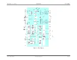
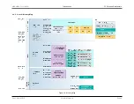
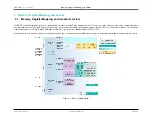
2.5 Memory
• Any of the USB endpoint buffers (since they are stored in the main SRAM area)
• The CRC engine
The PMU controller can also be used to read from the program flash memory or any peripheral register area which is normally accessible on the System bus. It does
not, however, have access to the USB control register area mapped to the AHB bus.
2.5.5
Flash Information Block
The flash information block on the
MAX32600
allows production trim values and other nonvolatile information that will be written during the production process (e.g.,
device configuration and test details / logging data) to be stored in a separate dedicated instance of internal flash.
The flash information block can be mapped to the AHB bus in the code space area, beginning at byte address location 0x0004_0000 (which is immediately following
the maximum possible flash memory address). This address location is constant even if a smaller flash memory size option is being used by the device.
When the flash information block is mapped to this memory region (between 0x0004_0000 and 0x0004_07FF), it can be accessed in the same manner as the
main flash; that is, it can be read from in code space (although accesses to it are not cached under any circumstances, and its contents are not subject to the
scrambling/descrambling function used by the contents of the main program flash memory). It is possible to write to locations in the flash information block using
either direct AHB writes (which will trigger a 32-bit write operation in the flash controller) or by writing the appropriate sequence directly to the flash controller registers.
However, this mapping of the flash information block (and direct read/write access to its contents) is only intended for testing and trimming purposes during the
factory production test sequence. Once production test of the
MAX32600
has completed (or at least the last stage where trim operations are performed has been
completed), a lock option setting will be set in the information block to prevent future modifications to the trim and option settings (except for those which are explicitly
allowed to be set later by the user, such as the DSB access key and the auto-lock security option). Setting the info block lockout setting also removes the information
block from the memory map, which means that the only way to view its contents after that point is by reading the copies of the info block settings that have been
copied by the hardware into the trim shadow registers (which are mapped to a different area in the APB peripheral region).
The flash controller automatically loads trim and other configuration values from the appropriate locations in the flash information block following any system reset.
To prevent misconfiguration of trim and other option settings in the case of a random (i.e., unprogrammed), blank, or corrupted information block, an "info block valid"
field is checked by the flash controller before the remaining locations in the information block memory are scanned. If the info block valid field (which is the first
addressed location in the information block array) does not match the predetermined "valid" key value (which is 0x12345678), the information block is presumed to
be invalid, and instead of the trim registers being set to copies of the data contained in the information block, they are loaded with predetermined "default" values
to prevent undesired or erratic system performance. These default values are designed to allow maximum access (with a minimum of security settings applied) for
ease of testing and configuration.
2.5.6
Flash Memory Controller
The flash memory controller on the
MAX32600
handles control and timing signals for programming and erase operations on both the main program flash memory
array and the flash information block. The flash information block is normally written during production test only, and is not generally intended to be modified by the
Rev.1.3 April 2015
Maxim Integrated
Page 15